Note: Descriptions are shown in the official language in which they were submitted.
CA 02307511 2000-05-04
577-425 PATENT
IMPROVED SMART CARD READER FOR ELEVATED PLACEMENT RELATIVE TO
A PRINTED CIRCUIT BOARD
FIELD OF THE INVENTION:
The present invention relates generally to an apparatus that electrically
connects an
integrated circuit (IC) card to a printed circuit board (PCB). More
particularly, the present
invention is directed to a smart card connector affixed at an elevation to a
PCB wherein the
connector supports a plurality of contacts in a top portion thereof. In this
configuration, the
connector not only preserves valuable PCB space for placement of additional
components
therebeneath but also obviates the requirement for an intermediate connector
portion for support
of electrical contacts thereinside.
BACKGROUND OF THE INVENTION:
In correlation with an increasing demand for diminutive electronic devices
capable of
multipurpose performance, the electronic industry has seen growth in the use
of flat plastic cards
incorporating computer chips therein. These chip or IC cards are also commonly
referred to as
"smart cards" and incorporate at least one electronic component to which
electrical connection
must be made. Smart cards, which often have compact size and shape
corresponding to
conventional credit and money-access cards, also include at least one contact
pad defined on a
surface thereof that establishes electrical connection to the electronic
components of a printed
circuit board (PCB). Smart cards are particularly adapted for use in
industries requiring strict
billing control and convenient access to money and information. Such
applications include
public phones, vending machines, copy machines, laundromat machines and
portable devices
such as mobile phones, pagers, laptop computers and similar electronic
devices. Such cards can
also be used in applications relating to health services, ticketing, security
access and machine
controls. In this disclosure, the terms "IC card", "chip card" and "smart
card" will be used
interchangeably to denote integrated circuit cards of this type.
1
CA 02307511 2000-05-04
In order to effect electrical connection between a smart card and a PCB, an
electrical
connector or smart card reader is employed such that the connector securably
accommodates the
smart card therein. The connector serves as an interface between a smart card
and a reading
system that interprets the information contained in the card.
The art has utilized numerous electrical connectors specifically designed for
use in
removably connecting various types of smart cards. An illustrative example of
a conventional
smart card reader is provided in Figure 1, wherein a smart card connector 10
includes a housing
12 fabricated from an insulative plastic and having a top portion 12a and a
bottom portion 12b
having dimensions circumscribed by a peripheral side wall 12c. Top portion 12a
and bottom
portion 12b together define a linear card insertion slot 14 having ingress 14a
through which a
smart card enters connector 10. Ingress 14a is generally sized and shaped to
correspond to a
smart card that is inserted therethrough.
Bottom portion 12b supports a plurality of electrical contacts 16 for
electrical
engagement with a contact pad of a smart card inserted thereagainst. Contacts
16 lie outwardly
from a mid-section of bottom portion 12b and have tail portions 16a that
extend normally
relative to peripheral wall 12c. Bottom portion 12b further includes one or
more securement
members 18 protruding from a bottom surface thereof for alignment and
securement of
connector 10 with a PCB. In order to ensure sufficient termination of contacts
16 to the PCB,
bottom portion 12b is positioned flush therewith.
Although the aforedescribed connector effectively establishes electrical
contact between
a smart card and a PCB, its use may not be desirable in configurations where
conservation of
materials and space is essential. The above design requires at least two
housing portions wherein
one portion must provide enough space for support of a requisite number of
electrical contacts
therein. Such configuration minimizes the amount of open space between the
connector and the
PCB, thereby sacrificing the ability to place additional components
therebeneath. This
configuration further limits the selection of card orientation during
insertion thereof into the
2
CA 02307511 2000-05-04
connector. Such limitations inhibit the use of the device within crowded PCB
configurations,
thereby contributing to increased costs associated with the manufacture of
such reading devices.
Thus, it is desirable to provide a smart card connector that establishes
electrical
communication between a smart card and a PCB while optimizing the available
PCB space for
placement of multiple components thereon. It is further desirable to provide a
smart card
connector that implements a contact configuration so as to effect a
satisfactory electrical
connection and enable visualization of a proper card insertion orientation.
SUMMARY OF THE INVENTION
It is an object of the present invention to provide a smart card connector for
insertable
accommodation of a smart card therein.
It is a further object of the present invention to provide a smart card
connector that
supports a smart card for movement into mechanical and electrical
communication with contacts
supported by the connector.
It is another object of the present invention to provide a smart card
connector that
optimizes available PCB space by enabling placement of additional components
beneath the
connector.
It is yet another object of the present invention to provide a smart card
connector that
enables a card reading operation to commence from a top portion of the
connector wherein all
electrical contacts are supported from a common termination side.
It is still another object of the present invention to enable visualization of
the proper
orientation of a smart card prior to insertion of the card into the connector.
In the efficient attainment of these and other objects, the present invention
provides an
electrical connector for connecting a contact pad of an IC card to a printed
circuit board. The
3
CA 02307511 2000-05-04
present invention is based on the problem of creating a reader for chip cards
in which available
PCB real estate is minimized by placing a card reading device directly
adjacent a PCB. The
present invention is also directed to the related problem of electrical
apparatus packaging,
wherein it is desirable to optimize use of available space to accommodate more
functions, and
thereby more components, in the apparatus. The present invention addresses the
need to increase
the available packaging space in the device to accommodate improvements
thereof.
By means of the present invention, a reader for smart cards is provided for
connecting
one or more contact pads of an IC card to the conductive elements of a PCB. In
particular, a
smart card connector is provided which elevates the connector above the PCB
for placement of
additional components therebeneath. The smart card connector of the present
invention includes
a housing having a lid and a base affixed thereto wherein the lid and base
together define a card
insertion ingress at a front portion of the connector. The ingress is sized
and shaped to
accommodate linear sliding insertion of a smart card along a card insertion
plane defined along a
card insertion slot that is circumscribed by the lid and base.
The connector lid supports a plurality of electrical contacts therein wherein
each contact
includes an inner extent having a spring-like undulation at a freely
deflectable interior extent
positioned in the card insertion plane. Upon card insertion, at least one
contact pad on the card
engages the interior extent such that the undulation deflects into a
corresponding recess defined
within the connector lid. Upon retraction of the card from the connector, the
undulation
resiliently returns to its original position in the card insertion plane. Each
contact further
includes an outer extent that protrudes normally from the connector lid for
termination to the
PCB. The contacts are desirably distributed in even and aligned rows that
enable placement of all
contacts in the connector lid.
4
CA 02307511 2009-02-10
In summary, therefore, the present invention generally provides a connector
for
establishing electrical connection between at least one contact pad of an
integrated circuit card
and conductive elements of a printed circuit board, comprising: a
substantially planar connector
housing supportable on the printed circuit board, the housing having a lid and
a base wherein
each of the lid and the base further includes an upper surface and a lower
surface defining a
thickness therebetween and wherein the lid and the base define a card
insertion slot therebetween
for insertably accommodating the integrated circuit card therein; a plurality
of electrical contacts
supported by the lid wherein each contact includes an interior contact extent
having a freely
deflectable spring-like portion defined thereat, the interior contact extent
provided for electrical
engagement with the contact pad of the integrated circuit card, and an
exterior contact extent for
termination to the printed circuit board; and at least one normally extending
offset member
protruding from the base lower surface for elevating the connector above the
printed circuit board
so as to define a predetermined height therebetween; wherein the lid includes
a pair of
longitudinally extending guide arms and the base includes a corresponding pair
of longitudinal
guide limbs extending from a central guide member such that the guide arms and
the guide limbs
together define card insertion rails along which the integrated circuit card
is guided until
insertion of the card into the slot.
4a
CA 02307511 2000-05-04
BRIEF DESCRIPTION OF THE DRAWINGS:
Figure 1 is a front perspective view of a smart card connector of the prior
art having a
plurality of electrical contacts supported in a bottom portion of the
connector housing.
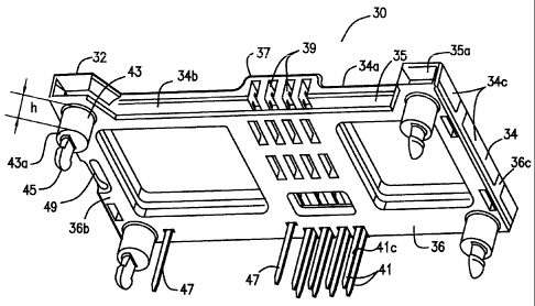
Figure 2 is a rear perspective view of a smart card connector of the present
invention.
Figure 2A is a front perspective view of the smart card connector of Figure 2.
Figure 3 is a front perspective view of a preferred embodiment of the smart
card
connector of the present invention.
Figure 3A is an alternate front perspective view of the smart card connector
of Figure 3.
Figure 4 is a top perspective view of a connector base of the smart card
connector of
Figures 3 and 3A.
Figure 4A is top view of the connector base of Figure 4.
Figure 5 is a top view of a connector lid of the smart card connector of
Figures 3 and 3A.
Figure 5A is a cross-section of the connector of Figure 5 taken along line A-
A.
Figure 5B is a rear view of the connector lid of Figure 5 showing a plurality
of electrical
contacts extending therefrom.
DETAILED DESCRIPTION OF THE PREFERRED EMBODIMENTS
The present invention provides for an integrated chip (IC) card connector that
establishes
an electrical connection between at least one contact pad on the card and
corresponding
conductive elements of a printed circuit board (PCB). The connector requires a
housing
CA 02307511 2000-05-04
fabricated from an insulative plastic. The housing includes a lid and a base
that together define a
card insertion plane therebetween having a card insertion ingress at a front
boundary thereof.
The connector lid supports a plurality of electrical contacts in even, aligned
distribution therein
so as to effect electrical engagement between the contacts and at least one
contact pad on the
card. In addition, at least one offset protrudes from a bottom surface of the
connector base. The
offset includes a securement element extending therefrom for attachment to the
PCB or other
support surface for the connector. The offset elevates the connector above the
PCB by a height
equal to the height of the offset, generating additional PCB space covering an
area equal to the
area of the bottom surface.
Now referring to Figures 2-5B, wherein like elements are identically numbered,
the smart
card connector of the present invention can now be described.
A smart card connector 30 of the present invention is provided in Figures 2
and 2A.
Connector 30 includes a housing 32 having each of a connector lid 34 and a
connector base 36,
each being molded from an insulative plastic. Lid 34 and base 36 together
define a card insertion
slot 35 therebetween wherein a smart card is linearly inserted along a card
insertion plane. A
card insertion ingress 35a bounds a frontmost portion of slot 35 and is sized
and shaped to accept
a correspondingly configured smart card therewithin.
Lid 34 is defined by a substantially planar upper surface 34a opposed by a
substantially
planar bottom surface 34b having side wall portions 34c depending therefrom.
Upper surface
34a is bifurcated by a contact hangar 37 having sufficient thickness to define
a plurality of
longitudinal recesses 39 therein. Recesses 39 correspond to a plurality of
electrical contacts 41
supported in lid 34 in aligned even distribution to effect proper mechanical
and electrical
engagement with all contact pads of a smart card.
. Each contact 41 includes an interior contact extent 41a (shown in Figure 5A)
having a
freely deflectable spring-like undulation 41b defined thereat for electrical
engagement with the
contact pad of a smart card inserted thereagainst. Each contact 41 further
includes an exterior
6
CA 02307511 2000-05-04
contact extent 41c for termination to the PCB. Each recess 39 accommodates
deflection of a
corresponding undulation 41b upon insertion of a smart card in slot 35. The
configuration and
operation of contacts 41 is further described hereinbelow.
Connector base 36 is defined similarly to connector lid 34 in that it has a
substantially
planar upper surface 36a opposed by a substantially planar bottom surface 36b.
Side latches 36c
depend normally from upper surface 36a and interengage corresponding
receptacles 34d in lid
34. The internengagement of lid 34 and base 36 as illustrated herein is merely
an example of one
type of configuration that can be implemented to secure lid 34 and base 36 to
one another. It is
therefore understood that other types of retention members can be employed
without departing
from the scope of the invention.
Base 36 further includes a plurality of offsets 43 protruding normally from
bottom
surface 36b toward a PCB (not shown) to which connector 30 is attached. Each
offset 43 has a
height h corresponding to a desired height at which connector 30 is elevated
above the PCB. An
offset 43 includes a substantially planar surface landing 43a at an extremity
thereof from which
an elongate securement member 45 extends. Securement members 45 are insertably
affixed
within a mounting aperture (not shown) in the PCB such that landing 43a lies
flush thereagainst
to define a component placement area beneath connector 30, such area having
height h. Such
height h is of sufficient dimension so that connected board mounted components
(not shown)
may be mounted to the board beneath connector 30.
Base 36 can also include one or more conventional switching contacts 47 to
indicate
complete insertion of a smart card within connector 30 and further initiate a
card reading
operation. Such switching contacts are well known within the art to execute a
card reading
operation and to control movement of a smart card during sliding insertion
thereof in the
connector. Base 36 may additionally include one or more retention fingers 49
formed integrally
therewith. Finger 49 presses against an edge of a smart card to ensure
alignment of the card
along the card insertion plane and further ensure securement of the card in
the connector once the
card is in a fully inserted card reading position.
7
CA 02307511 2000-05-04
Now referring to Figures 3 to 5B, a preferred embodiment of the present
invention can
now be described.
Figures 3 and 3A show alternate front perspective views of a smart card
connector 60 of
the present invention. Connector 60 includes a housing 62 fabricated from an
insulative plastic
material. Housing 62 includes each of a lid 64 and a base 66 interengaged with
one another via
securement of latches 66c with corresponding receptacles 64d. The
configuration of lid 64 and
base 66, respectively, is similar to that of lid 34 and base 66, respectively,
of connector 30 shown
in Figures 2 and 2A. Lid 64 is formed as a generally planar surface having
opposed upper and
lower planar surfaces 64a and 64b, respectively, which is bifurcated by a
contact hangar 67. In
addition, side wall portions 64c depend downward on lid 64 to create a wall
that, together with
latches 66c, circumscribes a card insertion slot 65 for sliding receipt of a
smart card therein.
Further referring to Figures 4 and 4A, connector base 66 includes a pair of
guide limbs 68
extending from a central guide member 66d. Each guide limb 68 includes an
offset 73
protruding from an undersurface thereof, such offset having construction
substantially similar to
that of offset 43 shown in Figures 2 and 2A. Each offset 73 includes a
substantially planar
surface landing 73a defined at an extremity thereof from which a securement
member 75
extends.
Base 66 is desirably molded so as to include a contact cell 84 having a
plurality of
passageways 86 therethrough. Passageways 86 accommodate insertion of
corresponding
contacts 41 inserted in connector 60 as further described hereinbelow. Cell 84
preferably has a
height corresponding to the height of offsets 73 so as to sit flush adjacent a
PCB or other support
surface. Such a configuration conceals the contacts within an insulative
housing, thereby
protecting them from damage and debris and reducing the opportunity for short-
circuiting.
Base 66 may further include one or more resilient retention fingers 79
integrally molded
therewith. Finger 79, like finger 49 of connector 30, presses against an edge
of a smart card
8
CA 02307511 2000-05-04
inserted thereagainst to retain the orientation of the card within connector
60 during a card
reading operation.
Base 66 is desirably molded to include a plurality of apertures 80 and 82
therein so as to
conserve materials and thereby reduce the cost of connector manufacture. An
aperture 84 is also
desirably included in which one or more switching contacts 77 are positioned.
Switching
contacts 77 are shown herein as deflectable spring-like contacts in an
opposing cantilever
configuration. Switching contacts 77 are conventional contacts that initiate a
card reading
operation when a smart card edge is inserted thereagainst. The contacts may be
disposed in a
normally open configuration as shown herein such that a card reading operation
begins upon
engagement of the contacts' deflectable ends. Alternatively, the contacts may
be disposed in a
normally closed configuration wherein a card reading operation commences as
soon as a smart
card engages a contact most proximate thereto. As stated hereinbefore, the
configuration and
disposition of switching contacts 77 is well known in the art.
As further illustrated in Figures 5, 5A and 5B, connector lid 64 is provided
with guide
arms 68' that correspond in length and width to guide arms 68 of connector
base 66. Guide arms
68 and 68' together define card insertion rails 90 along which a smart card is
guided until
insertion of the card into slot 65. Rails 90 ensure proper linear sliding
movement of the card
during insertion or retraction thereof, yet also allow the user to easily view
the card to determine
if the contact pads of the card are in a proper card reading orientation
relative to the connector.
Lid 64, like lid 34 of connector 30 shown in Figures 2 and 2A, provides a
plurality of
longitudinal recesses 69. As specifically shown in Figure 5A, each recess 69
accommodates
disposition of at least one contact 41 therein. Each contact 41 has a freely
deflectable interior
extent 41 a as shown with a spring-like undulation 41b at an extremity
thereof. Each contact 41
also includes an exterior extent 41b having a 90 bend relative to lid 64 for
simple termination to
the PCB. Contacts 41 are provided in an even, aligned distribution wherein
each contact is
separated from an adjacent contact by a predetermined distance d (shown in
Figure 5B). This
distribution of the contacts in lid 34 easily accommodates all of the contacts
in a single housing
9
CA 02307511 2000-05-04
piece and ensures predictable engagement between the contacts and the contact
pads of a smart
card inserted in the connector.
In operation, connector 60 is attached to a PCB or other support surface by
removably
attaching securement members 75 to the PCB so that offset landings 73a are
positioned directly
thereadjacent. Offsets 73 thereby elevate connector 60 above the PCB by a
height h'
corresponding to the height of the offsets themselves. Additional electrical
components can
therefore be placed underneath the connector to accommodate plural functions
for an electronic
device within which the connector is installed. The connector thereby
preserves valuable PCB
space while ensuring a sufficient electrical connection during a card reading
operation.
A smart card is inserted into connector 60 with a surface of the card defining
the contact
pads thereon facing upward toward interior contact extents 41 a. Insertion of
the card begins by
aligning the card within rails 90 and pushing the card in a card insertion
direction designated by
arrow A. Rails 90 guide the card toward ingress 65 for introduction of the
card along the card
insertion plane into card insertion slot 65. The card continues sliding
movement toward a rear
portion of connector 60 such that interior contact extents 41a contact the
surface of the card, and
thus the contact pads thereon. Continued sliding movement of the card deflects
undulations 41b
upward into corresponding recesses 69 and they are retained therewithin for
the duration of a
card reading operation. Upon retraction of the card from slot 65, undulations
41b resiliently
return to their original resting position within the card insertion plane. It
is noted that sliding
movement of the card during insertion may be limited by either or both of
switching contacts 77
once the card comes into mechanical and electrical engagement with such
contacts.
It is evident from the foregoing description that the present invention is
useful for various
applications wherein preservation of PCB space is allocated a high priority.
The present
invention does so without compromising valuable packaging areas or sacrificing
sufficient
electrical connection between the smart card and the PCB.
CA 02307511 2000-05-04
Various changes to the foregoing described and shown methods and corresponding
structures would now be evident to those skilled in the art. The matter set
forth in the foregoing
description and accompanying drawings is therefore offered by way of
illustration only and not
as a limitation. Accordingly, the particularly disclosed scope of the
invention is set forth in the
following claims.
11