Note: Descriptions are shown in the official language in which they were submitted.
CA 02307880 2000-04-27
WO 99/22266 PCT/US98/22817
-1--
DISCRETE ELEMENT L1GHT MODULATING MICROSTRUCTURE DEVICES
TECHNICAL FIELD
The present invention relates generally to light modulators and light
switches, and
more particularly to electro-optic modulator arrays. The inventor anticipates
that primary
application of the present invention will be in high-speed printing and image
processing,
although it may also be used in optical interconnects, telecommunications and
flat panel
displays.
BACKGROUND ART
Electro-optic modulators have been well known in the art for years, but for
multi-
channel applications they have suffered from several disadvantages. Prior art
modulator
arrays have usually been formed from single wafers of electro-optically active
material onto
which surface electrodes have been attached, to form channels which are
defined by the
electric field lines within the optical wafer. Cross-talk, or interference
between channels, has
been a problem because electro-optic modulators are vulnerable on at least two
levels. Since
the channels are not restricted except by the electric field lines, activity
in one channel can
easily induce electro-optic interference in a nearby channel. This is in
addition to usual
electrical cross-talk experienced by closely grouped and unshielded electrical
contacts. Also,
previous electro-optic modulators and light switches have often relied on
surface deposited
electrodes, which produce electric field lines that are fringed, rather than
channeled and
directed. Due to the exponential decay of the electric field intensity inside
the material, very
high voltages may be required to drive the material to produce the desired
electro-optic
effect.
Electro-optic materials, such as LiNb03, can be expensive, and can require
high
driving voltages. Liquid crystal modulators have also been used, but response
times for this
type are typically very slow, on the order of milliseconds. Also, the electro-
optic effect
exhibited by a material can be of several different orders, depending on the
material. A first
order effect, called the Pockels effect, is linear in its response to increase
in applied voltage."
A second order effect, called the Kerr effect, is quadratic in its response,
thus a greater
increase in effect can be produced relative to an increase in voltage. This
can theoretically
CA 02307880 2000-04-27
WO 99/22266 PCTNS98/22817
-2-
allow smaller driving voltages in a primarily Kerr effect material to be
applied to produce a
comparable electro-optic effect compared to material which produces primarily
Pockels
effect.
Lead zirconate titanate polycrystalline ceramic which is doped with lanthanum
(PLZT) is a relatively inexpensive, optically transparent ceramic which can be
made to
exhibit either the quadratic Kerr effect or the linear Pockets effect,
depending on the
composition, and can be formed into wafers easily and used in sot-gel
moldings. The
concentrate of lanthanum, or "doping", is variable, and can lead to varying
characteristics in
the material. PLZT that is commercially available is typically made from a
"recipe" which
produces a very high dielectric constant K. Very high K values produce high
capacitance
values C, which in turn produce high power requirements, as power (P) is
proportional to
CVZ/2 where V = voltage. High power consumption in turn generates heat, so
that some
modulators that require high voltage also may require cooling. If the
proportion of
lanthanum dopant, or other components, in the material is adjusted, the
dielectric constant
value and electro-optic constant value, as well as the type of electro-optic
effect (Kerr or
Pockets), may also be varied, with the result affecting capacitance and power
consumption.
Prior art inventions for modulating light in arrays generally suffer from
common
problems experienced by multi-channel optical and electrical systems in which
the channels
are not appropriately isolated. As discussed above, interference is easily
induced in nearby
channels resulting in cross-talk which can distort image clarity and corrupt
data
transmissions. Additionally, much of the prior art requires high driving
voltages that are
incompatible with TTL level power supplies.
U.S. Patent No. 4,746,942 by Moulin shows a wafer of PLZT electro-optic
ceramic
material with a large number of surface mounted electrodes. This invention
suffers from the
disadvantage of cross-talk between channels, although there is discussion of
attempts to
decrease cross-talk by use of large electrodes and increased space of the
electro-optic
windows. This results in less efficient use of the material. Although typical
driving voltages
are not given, with larger areas of material, higher applied voltages become
necessary to
provide the necessary electric field density in the wafer.
U.S. Patent No. 4,867,543 by Bennion et al. describes a spatial light
modulator made..
of a solid sheet layer of electro-optic material such as PLZT, which has
paired surface
electrodes, This has the disadvantage of requiring a driving voltage of
approximately 20
volts to produce a phase retardation of Pl radians. U.S. Patent No. 4,406,521
by Mir et al.
CA 02307880 2000-04-27
WO 99/22266 PCT/US98/22817
3-
discloses a panel of electro-optic material which uses electrodes to define
pixel regions. It
speaks of using voltages in the range of 100 - 200 volts. U.S. Patent No.
5,033,814 by
Brown et al. also shows a single slab of electro-optic material which requires
a driving
voltage of 150 volts. U.S. Patent No. 5,528,414 to Oakley discloses a single
wafer of Pockels
crystal with surface mounted electrodes requiring a 70 volt driving voltage.
Besides being
obviously incompatible with TTL voltage levels, none of these inventions have
any
mechanism for confining electric field lines. Also, in general, use of higher
driving voltages
will generate heat in the eiectro-optic material, which can mean that a
cooling system may be
required.
U.S. Patent No. 5,220,643 by Copings discusses an array of optical modulators
which
are built into a neural network. These modulators are mostly of liquid crystal
type, although
use of PLZT is mentioned. U.S. Patent No. 4,560,994 by Sprague shows a single
slab of
electro-optic material with an array of electrodes which create fringe
electric fields, which are
not channeled. Sarraf's U.S. Patent No. 5,521,748 also discloses a modulator
array in which
mirror-like devices deflect or deform when electrostatic force is applied.
U.S. Patent No.
4,367,946 to Varner also discusses a light valve array, with one specifically
preferred
material being PLZT. However, all four of these inventions can be expected to
have the same
problems of cross-talk, which the present invention is designed to eliminate.
For the foregoing reasons, there is a need for an array of discrete light
modulating
elements which can operate at TTL voltage levels, and at high speeds, with
almost no cross-
talk, and which can be used to produce small pixels or which can be grouped
together to
create larger pixels and large two dimensional panels or sheets.
DISCLOSURE OF THE INVENTION
Accordingly, it is an object of the present invention to provide an array of
discrete
modulated elements of eiectro-optic material.
Another object of the invention is to provide arrays of electro-optically
modulators
that can be driven by TTL voltages, and thus be compatible with standard TTL
power
supplies.
Yet another object of the invention is to produce arrays of electro-optic
modulators
which have very little cross-talk between channels.
CA 02307880 2000-04-27
WO 99/22266 PCTNS98/Z2817
-4-
Still another object of the present invention is to provide an array with very
fast
response and switching time.
A further object of the present invention is to provide an array of pixels
which can be
of very small dimensions to reduce problems of aliasing in optical displays.
A yet further object of the present invention is to produce light modulating
arrays that
can be manufactured by conventional methods very inexpensively.
Briefly, one preferred embodiment of the present invention is a light
modulating array
having a number of discrete protrusions formed of electro-optic material, each
of which is
electrically and optically isolated from each other. The protrusions each can
be viewed as
having a top face, a bottom face, first and second side faces, and front and
back faces. Each
array also has a number of electrodes associated with each of the protrusions,
the electrodes
being capable of inducing an electric field in the electro-optic material for
independently
modulating a number of light beams which are incident upon one of the faces of
the
protrusions. The protrusions can be made from any number of electro-optic
materials
including electro-optic crystals, polycrystalline electro-optic ceramics,
electro-optically
active polymers, electro-optic semiconductors and electro-optic glasses. The
protrusions can
be integral with a substrate wafer, or formed upon a substrate of a second
material. The
electrodes can be attached in a variety of positions including on the sides,
top and bottom,
and on the front and back faces if electrodes with apertures are used.
A second preferred embodiment of the present invention is a light modulating
array
having a number of discrete protrusions formed of electro-optic material, each
of which is
electrically and optically isolated from each other, each protrusion being
formed in a prism
shape. Each protrusion has a top face, a bottom face, and front and rear
faces. Each array
also has a number of electrodes associated with each of the protrusions, the
electrodes being
capable of inducing an electric field in the electro-optic material for
independently
modulating a plurality of incident light beams. Each of the prism shaped
protrusions is
oriented with respect to a number of light beams such that each light beam
incident upon the
front face of each protrusion enters the protrusion traveling a first path and
emerging at a first
angle from the rear face of the protmsion when no voltage is applied to
electro-optically ,
activate the protrusion. However, each light beam travels a second path and
emerges at a
second angle from the rear face of the protrusion when the protrusion is
electro-optically
activated by application of appropriate voltage.
CA 02307880 2000-04-27
WO 99/22266 PCT/US98/228I7
-5-
A third preferred embodiment of the present invention is a light modulating
array
having a matrix of electro-optic material, with each matrix containing a
number of embedded
adjacent electrodes. The electrodes are each capable of inducing an electric
field in the
electro-optic material for independently modulating a number of light beams
which are
incident upon the matrix of electro-optic material.
A fourth preferred embodiment of the present invention is a system for
modulating
light having a number of discrete protrusions formed of electro-optic material
and a number
of electrodes, as above. The system also includes a power supply capable of
supplying
sufficient voltage to induce a desired polarization shift from a first
polarization orientation to
a second polarization orientation in a beam of polarized light entering the
protrusions. Also
included are a switches for controlling application of voltage to the
electrodes through a
conductor and a separator for separating light of a first polarization
orientation from light of a
second polarization orientation. The separator could be any of a number of
mechanisms,
such as beam splitters, cross-polarizers, etc.
An advantage of the present invention is that it may be operated with TTL
voltages or
lower.
Another advantage of the invention is that because of the low voltage
requirements,
heating of the elements is reduced and requirements for cooling are minimized.
Yet another advantage of the present invention is that very small elements may
be
produced, thus allowing for very fine image resolution.
A further advantage of the present invention is that cross-talk between
channels is
nearly eliminated.
A still further advantage of the present invention is that standard micro-
machining
operations can be used, allowing for inexpensive manufacture.
A yet further advantage of the present invention is that sol-gel processes can
be used
to create arrays very inexpensively.
Yet another advantage of the present invention is that sol-gel processes can
be used to
make displays which are both thin and flexible. These molding processes can
produce arrays
with large numbers of elements quickly and for very low cost.
These and other objects and advantages of the present invention will become
clear t,Q
those skilled in the art in view of the description of the best
presently~known mode of
carrying out the invention and the industrial applicability of the preferred
embodiment as
described herein and as illustrated in the several figures of the drawings.
CA 02307880 2000-04-27
WO 99/22266 PCT/US98/22817
BRIEF DESCR1PT10N OF THE DRAWINGS
The purposes and advantages of the present invention will be apparent from the
following detailed description in conjunction with the appended drawings in
which:
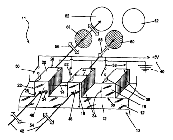
FIG. 1 is a perspective view of a system for modulating and switching light
beams
which uses a light modulating array, showing the modulation of impinging light
beams;
FIG. 2 is a perspective view of a modulator array, and electrical circuit
showing an
alternative location for conductive pads;
FIG. 3 is a perspective view of a modulator array, and electrical circuit
showing the
elements mounted on a substrate of different material;
FIG. 4 is a perspective view of a modulator array and electrical circuit in
which
electrodes have been attached to the top and bottom wafer surfaces;
FIG. 5 is a perspective view of a modulator array and electrical circuit
showing an
alternate location for conductive pads;
F1G. 6 is a perspective view of an alternate embodiment of a modulator array
and
electrodes;
FIG. 7 is a perspective view of another alternative embodiment of a modulator
array
and electrodes;
FIG. 8 is a perspective view of system for modulating and switching light
beams
Which uses a modulator array and beamsplitters to separate modulated and
unmodulated
beams into different channels;
FIG. 9 is a plan view of a system for modulating and switching light beams,
which
shows a single element of a modulator array used as an alternate mechanism for
separating
modulated and unmodulated beams into different channels;
FIG. 10 is a perspective view of a system for modulating and switching light
beams
which shows a single element of a different version of a modulator array used
as an alternate
mechanism for separating modulated and unmodulated beams into different
channels;
FIG. 11 is a perspective view of a modulator array in which electrodes have
been
placed so as to produce an electric field which is collinear with the
direction of light
propagation; and
FIG. 12 is a cross-sectional view of an embedded electrode array in a sot-gel
matrix of
electro-optic material.
CA 02307880 2000-04-27
WO 99/22266 PCT/US98/22817
BEST MODE FOR CARRYING OUT THE INVENTION
A preferred embodiment of the present invention is an array of light
modulating
and switching microstructure devices. The present invention solves many of the
problems of the prior art by using lanthanum doped lead zirconate titanate
crystal
(PLZT), which is an optically transparent ceramic that becomes birefringent
when
proper voltage is applied. PLZT has a quadratic electro-optic response to
voltage
increase thus allowing lower driving voltages. In addition, the present
invention uses an
optimized compositional "recipe" in which the proportion of lanthanum dopant
and
matrix elements has been designed to produce low dielectric constant K, higher
electro-
optic efficiency, and thus low power requirements. Additionally, the electro-
optic
elements are 3-dimensional and of very small size, generally lOpm - 200um in
the light
propagation direction, or much less, depending on the design. This allows
production
of very high-density electric fields in these elements by using small
voltages, including
TTL levels of approximately 5 volts, and lower. This has advantages because
power
supplies that are already set up for TTL level digital components can supply
the electro-
optic modulators as well. Cross-talk has been nearly eliminated by the use of
grooves
or regions which are filled with air or other dielectric materials. These
physically
separate at least a portion of the elements, thus directing and channeling
electric field
lines more closely. PLZT, as well as other electro-optic materials, also
allows for pico-
second response time, thus theoretically allowing very high switching
frequencies of
100 GHz and more.
The use of embedded electrodes produces more uniform electric field strength
in the
elements. This allows a much lower driving voltage and a much more predictable
and
controllable electric field.
The present invention is also useful when using standard recipe electro-optic
materials, in which the dielectric constant has not been minimized, and also
in a variety of
other electro-optic materials beside PLZT. Electro-optic materials fall
generally into five
categories, 1 ) electro-optic crystals, 2) polycrystalline electro-optic
ceramics, 3) electro-
optically active polymers, 4) electro-optic semiconductors, and 5) electro-
optic glasses.
Although the electro-optic properties of the materials are variable defending
on composition,
the present invention can be implemented with materials of any of these three
categories.
Specific examples of electro-optic materials besides PLZT which may be used
include, but
CA 02307880 2000-04-27
WO 99/22266 PCTNS98/22817
-g-
are not limited to, LiNbO~, LiTaOz, BSN, PBN, 1<TN, KDP, KD*P, KTP, BaTiO~,
BazNaNbsW s. GaAs, InP, CdS, AgGaSz, and ZnGePz. The very small dimensions of
the
elements result in very low element capacitance even when using material
having a relatively
large dielectric constant x.
As illustrated in the various drawings herein, and particularly in the view of
FIG. 1, a
form of this preferred embodiment of the inventive device is depicted by the
general
reference character 10.
FIG. 1 illustrates an array of light modulating microstructures 10 as well as
a system
11 for modulating or switching light in a number of independent channels. In
this preferred
embodiment, the array 10 is formed from a wafer l2 of PLZT. PLZT has been
chosen for its
large electro-optic effect and low absorption for thin wafers.
If PLZT is used, the relative proportion of the Lanthanum dopant in the
ceramic can
be very important in determining the driving voltage required for the
elements. The
composition also is important in establishing the optical properties such as
transparency,
grain size and pore size, speed, power dissipation, operating temperature and
for maximizing
both the linear and the quadratic electro-optic coefficients of the material.
Commercial
recipes for PLZT have largely used Lanthanum concentrations of 9.0% to 12%. If
Lanthanum concentration is varied in the range of 8.5% to 9.0% of the PLZT
ceramic and the
concentration of Zirconium and Titanium are unchanged from typical ratios of
65/35, it may
be possible to achieve a higher quadratic electro-optic coefficient (R) in the
PLZT for the La
dopant percentage closer to 8.5°io. For the PLZT compositions, where Zr
and Ti are
maintained in a 65/35 ratio and the overall percentage of La is varied:
La = 9.5%, R = 1.5 x I 0'"' mz/Vz;
La = 9.0%, R = 3.8 x 10'"' mz/Vz.
It is known that for La < 8.0%, PLZT loses quadratic electro-optic properties.
It is therefore
expected that somewhere around 8.5% La there should be a maximum for R around
(S-40) x
1 pu ~ mz/V2
This enhanced value of electro-optic coefficient provides many advantages. It
will
permit lower required driving voltages, and thus lower power dissipation in
the material and
hence lower heating of the device. This in turn allows the device to be driven
at significantly
higher frequencies, even without external cooling. Also, the use of lower La
concentrations
(which is a free electron donor) will result in a reduced "charge screening"
effect. The
overall result is higher modulation efficiency of devices manufactured from
this material.
CA 02307880 2000-04-27
WO 99/22266 PCT/US98/22817
The wafer 12 has regions or grooves 14 formed to produce protrusions 16 from
the
original thickness 18 of the wafer 12. The grooves 14 may be formed by any
number of
means, such as mechanical machining with micro-saws, chemical etching using
photo-resist
masks, or laser ablation, or the array may be molded in shape from
polycrystalline ceramic,
among other methods. The grooves 14 provide isolation between the channels of
the array
10, serve to direct and channel the electric field lines in the electro-optic
material and thus
allow the array to operate with nearly zero cross-talk.
Each protrusion 1G has a top face 20, a first side face 22 and a second side
face 24, a
front face 2G and a rear face 28. The grooves l4 can be cut through the entire
original
thickness 18 ofthe wafer 12, in which case, the protrusions will have an
independent bottom
face 30, or if the groove is not cut through the entire original thickness 18,
the bottom face 30
will be integral with the wafer 12, as shown by the dotted line in Figure I.
The faces of the wafer 32 can be polished either before or after the grooves
14 are
formed, to prevent scattering of light entering or leaving the wafer 12.
Electrodes 34 are
attached to the protrusions 1 G by any of a number of ways, but one preferred
method is to
embed the electrodes 34, as this may produce a more uniform electrical field.
It is also
possible that the material of the electrode 34 may completely fill the grooves
14. Conductive
pads 3G of gold or some other metal or conductive material are used to attach
electrical leads
38 to the electrodes 34, which connect them in turn to the electrical power
supply 40. An
electrical field is thus established which is oriented in a transverse
direction relative to the
direction of the incoming light beams 42. The width of electro-optic material
between the
grooves 14 in the protrusions 1G establishs the electrode gap 44 in this
configuration of
electrode 34 placement.
For ease of reference, an assembly containing a protrusion 1G, attached
electrodes 34,
and conductive pads 3G shall be referred to as an "element". The size of the
wafer 12, the
protrusions IG and the electrode gaps 44 will depend on the material chosen,
and the desired
range of applied voltages to be used. The electro-optic effect exhibited by an
element of a
particular material depends on the electric field strength within that
element. The density of
that field will in turn depend on the amount of applied voltage, the material
chosen, and the
physical dimensions of the element in which the electric field is contained.
Using very smajl
elements allows a large concentration of electric field density by use of
small to moderate
voltages. In the present invention, in order to use voltages in the TTL range,
around SV, it is
estimated that the physical size of the elements, if made of PLZT, will be on
the order of 20
CA 02307880 2000-04-27
WO 99/22266 PCTNS98/22817
-10-
pm x 20 pm x 200 pm. The grooves 14 can be made very small, and indeed may be
limited
by the size of machining tools used to form them. 1~xcellent results in terms
of near zero
cross-talk have been achieved using micro-sawing methods where the kerf size
of the saw
cuts are around 25 pm. Effective reduction of cross-talk between channels may
be achieved
with grooves as small as 5 Itm.
Such tiny elements can produce modulated beams of very small size, producing
such
fine image resolution that the unaided eye is incapable of distinguishing it.
It may have
applications where microscopic images are required, or where multiple beams
are combined
in groups of S or 10 elements to make up 1 pixel in a display device.
The size of the elements will also depend on whether the beam is transmitted
through
the element or reflected from a rear surface, in which case, the length or the
driving voltage
can be cut roughly in half to produce the same degree of modulation. Materials
with smaller
electro-optic properties may require greater size or increased applied voltage
to achieve
proper modulation results.
I S In Fig. I, a first element 4G and a second element 48 are shown, which in
this
preferred embodiment, will be assumed to be composed of PLZT. Between the
first element
4G and the voltage supply line, an open switch 50 is shown to represent that
the element 4G
has no voltage applied, and is in an inactive state. It is, of course, to be
understood that
nothing so primitive as throw-switches need be used to practice the invention.
Most likely,
very high frequency (perhaps as much as I 00 GI-Iz or more) square waves of
appropriate
voltage will be used, but throw-switches are used here as an easy means of
illustrating the
state of the applied voltage.
The incoming light beams 42 having incoming linear polarization 54 which is
aligned
with the upper tip 45 degrees to the left of vertical, (which shall be
referred to as "R"
polarization) impinge on bath elements 4G and 48. This incoming light may be
linearly
polarized laser light, or it may be initially unpolarized light, perhaps even
including light
from an incandescent bulb, which has been transmitted through a polarizer to
produce
linearly polarized light. First element 4G is inactive, thus the outgoing
polarization SG of the
first element 4G is unchanged. It passes through an R aligned polarizer GO and
is detected by
a light sensor or photo detector G2, perhaps to be recognized as a digital
"1".
In contrast, switch 52 is closed leading to the second element 48, thus the
supply
voltage is applied and the element 48 is active. The element 48 becomes
birefringent under
the influence of the applied electric field. Birefringence causes an incoming
beam 42 which
CA 02307880 2000-04-27
WO 99/22266 PCTNS98/22817
is linearly polarized at a 45 degree angle relative to the direction of the
applied electric field
to split into two orthogonal components which are respectively parallel and
perpendicular to
the electric field lines. These components travel along the same path but at
different
velocities. The electro-optic effect thus will cause a phase shift between the
two components,
as one is retarded in relation to the other. After traveling through the
element 48, the
components re-combine with the result that the polarization of the emergent
beam 58 is
changed. If the voltage is sufficient to cause a ~,/2 shift in polarization,
the polarization will
be rotated by 90 degrees, relative to its original orientation. In FIG. l, it
is assumed that a 7.,/2
voltage of 5 volts has been applied which produces a 90 degree phase shift to
give a linearly
polarized output beam 58, which is oriented with the upper tip now 45 degrees
to the right of
vertical (which shall be referred to as "S" polarization). This S polarized
light is now
blocked by the R aligned polarizer G0, which allows no light to reach the
detector G2. This
may be recognized by a digital device as a "0".
If the applied voltage causes a ~,/4 rotation, the outgoing polarization 58
will be made
into circular polarization, as the tip of the resuitant electric field vector
will describe a circle
as it propagates. Intermediate voltage values will result in elliptical
polarization. These will
be incompletely blocked by the polarizer G0, which will allow only the R
aligned component
to pass. Thus, the tight seen by the detector G2 may be theoretically
controlled anywhere in
the range from undiminished incoming intensity to total extinction, to produce
analog-type
output signals if the appropriate control voltage is applied.
FiG. 2 illustrates a different version of the modulator array 10. A wafer 12
is shown
with attached or embedded electrodes 3:1, and in this embodiment, the
conductive pads 36 are
located in a different configuration for attachment to electrical leads 38.
FIG. 3 illustrates another version of the modulator array 10, in which the
grooves 14
have been extended completely through the original thickness 18 of the wafer.
The elements
G4 here are composed of the protrusion 1 G portions of the wafer 12 and their
respective
attached or embedded electrodes 22 and conductive pads 24 (see FIG.1 ). A
number of
elements G4 have been formed on a substrate GG made from a different material
which the
bottom faces 30 now contact. This substrate GG is preferably a low dielectric
material that is
not electro-optically active, such as SiO~, for one example among many. The
protrusions 1G
may be attached or glued to the substrate GG prior to machining or attachment
of the
electrodes 34 and pads 3G, or the completed elements G4 may be assembled prior
to
attachment to the substrate GG.
CA 02307880 2000-04-27
WO 99/22266 PCTNS98/22817
12-
FIG. 4 shows yet another version of the modulator a~Tay 10. In this
embodiment,
electrodes 34 are attached to the top faces 2U of the protrusions IG and a
single large
electrode G8 is positioned on the bottom side 70 of the wafer 12. It is to be
understood that a
plurality of appropriately placed individual electrodes could be used on the
bottom side 70 of
the wafer 12 in place of the single large electrode G8 pictured here and in
the following FIG.
S. Conducting pads 3G are attached to the top and bottom electrodes 34, GS as
attachment
points for the electrical leads 38. Polished front faces 2G are indicated as
before, and
incoming light beams 42 are shown to indicate orientation. The polarization
direction has not
been shown, as the principles of phase retardation operate much the same as in
FIG. 1, with a
~./2 shift producing a 90 degree rotation, etc. This placement of electrodes
34, G8 produces a
different orientation of transverse electrical fields, but still retains the
advantage of channel
separation and minimization of cross-talk which was unavailable in the prior
art.
FIG. 5 shows a variation of the configuration in FIG. 4, in which the upper
conductive
pads 3G are located in a different orientation relative to the wafer 12. The
top and bottom
electrodes 34, G8 are positioned as in FIG. 4, to produce a transverse
electric field. The
polished front faces 2G and incoming light beams 42 are again shown for
orientation
purposes.
Although not pictured here, it is to be understood that this arrangement of
top and
bottom electrodes and the variations in conductive pad locations seen in FIGS.
4 and 5 can be
used with elements which have been positioned on a different substrate
material, in the
manner suggested by FIG. 3, if the substrate material has the proper
conductive properties. It
may also be possible for elements to be directly attached to a single large
bottom electrode
which can act as a substrate to support and position the elements.
Alternately, the electrodes
may be attached or embedded on both sides of the electro-optic material
directly before
mounting the assembled elements onto a substrate.
FIG. 6 shows another version of an array 10 of modified protrusions 72 which
have
either been formed on the original wafer 12 or formed separately on a
substrate of different
optically transparent material GG in a similar manner to the embodiment shown
in FIG. 3.
The modified protrusions 72 are shown to be oriented with their long sides
parallel to the
long edge of the wafer 12 or substrate GG, but it should be understood that
they may also be,.,
oriented with the long sides of the protrusions 72 transverse to the lord edge
of the wafer 12
or substrate GG. An incoming polarized light beam 42 enters from the bottom
side 70 of the
wafer 12 or substrate GG and is internally reflected on the angled first side
face 74 and angled
CA 02307880 2000-04-27
WO 99/Z2266 PCT/US98/228I7
-13-
second side face 7G to reemerge from the bottom side 70 of the wafer 12. If
appropriate
voltage has been applied to the electrodes 78, the resulting polarization of
the emergent light
beam 80 will be modulated in the manner described above. The angles of the
faces here are
chosen to allow total internal reflection, but it is to be understood that if
a reflective coating is
S applied to the faces, a variety of other angles may be used as well.
FIG. 7 illustrates yet another version of a modulator array 10 in which the
protrusions
82 have been modified in another manner such that the angled second side face
84 of each
has been angled to direct the emergent beam 8G out of the top face 20 of each
protrusion 82.
As in FIG. 6, the protrusions may be oriented in a transverse direction, a
different substrate
material may be used, and a reflective coating may be applied to reflecting
faces.
FIG. 8 shows a system 11 for modulating or switching light beams which uses
the
modulator array 10 in much the same configuration as in FIG. 1. An incoming
linearly
polarized beam 42 of polarization "R" enters a first element 4G which is
inactive due to an
open switch 50, so that its exiting polarization 5G is unchanged. This enters
a beamsplitter 88
that has been positioned so that light of R polarization will be reflected out
of the
beamsplitter at angle ~, as shown by reflected beam 90. In a second element
48, which is
active, the voltage is assumed to be such as to produce a ~./2 shift, the
polarization is rotated
90 degrees to "S" orientation, and this passes through the beamsplitter 88, as
shown by
unreflected beam 92. These beams can be used to carry separate digital
information, and may
be designated "channel 1" 94 and "channel 2" 9G. It is to be understood that
beamsplitters
can be used as a channel separation device with any of the various embodiments
illustrated
herein.
FIG. 9 shows a top plan view of another system 11 for modulating or switching
light
beams which uses a different version of a light modulating array 10. A single
protrusion 1G
is shown, which is composed of a first blocl: 98 or portion of material having
an index of
refraction N,, and a second block 100 of material having index of refraction
NZ. A boundary
102 is formed at the junction of the two materials. One of the two blocks, in
this case the first
block 98, has top and bottom electrodes 104. First blocl: 98 is composed of
electro-optic
material such that when electrodes 104 are uncharged, the electro-optic
material is inactive,
and N, = N~. When voltage is applied to electrodes 104, the first block 98
becomes active
and the index of refraction changes for polarization components which are
aligned with the
electric field lines so that for this polarization, N> > N,. When first block
98 is inactive, an
incoming beam lOG is projected into the first block 98 at entry angle s to a
normal such that
CA 02307880 2000-04-27
WO 99/22266 PCT/US98/22817
-14-
the beam passes through the boundary between the two blocks 98, 100 and
emerges as
unreflected light ray 108. When first block 98 is active the index of
refraction is increased
such that total internal reflectance (TIR) occurs, and the beam is reflected
back into the first
block 98 at the boundary 102, and emerges as reflected light ray 110. The two
emergent
beams 108 and 110 are separated by angle 8, which has been greatly exaggerated
here. These
separated beams 108, 110, can be detected by sensors 112, and thus be used to
establish
channel separation for data transmission.
Alternatively, the protrusion 1G can be made from a single integral block of
material,
which has been electro-optically divided into portions or sections. A first
section 98 may
have electrodes 104 attached to induce a different index of refraction in this
section: An
incoming beam l OG will then be totally internally reflected, as described
above, at the
interface between the activated 98 and unactivated sections 100. This
interface or boundary
102 can be established more definitely by having the second section 100, be of
a different
thickness than the first 98. This serves to direct the electric field lines
better so that less
fringing is produced, and a sharper interface boundary 102 is established.
FIG. 10 shows a perspective view of another system 11 for modulating or
switching
light beams which uses yet another version of the light modulating array 10 to
perform
channel separation. A single prism-shaped protrusion 114 is shown, which can
be electro-
optically activated by electrodes 1 IG to increase the index of refraction.
This causes the light
beam to be bent towards the normal upon entry slightly differently than when
the material is
an inactive state. Thus when the element is active, the light beam will follow
a first path 118,
and will emerge at a slightly different angle relative to the normal upon
leaving the element,
thus following a first exiting path 120. In contrast, when the element is
inactive, the light
follows a second path 122 upon entry, and follows a second exiting path 124.
Both of these
second paths are shown in dashed line in Figure 10. These first and second
exiting paths 120,
124 are separated by angle (3, and they can be further directed by mirrored
surfaces 126 to
sensors 128 to produce separate channels. The separation ofthe paths and the
separation
angle has been exaggerated in the Figure 10.
FIG. 11 illustrates yet another version of the present light modulating array
10 in
which end-mounted electrodes 130 each having an aperture 132 have been
attached to the =-
front faces 2G and rear faces 28 ofthe protrusions IG. In this configuration,
the electric field
lines are collinear with the direction of II1C0111111~ light beams 42. The
application of
appropriate applied voltage results in the chan;e in polarized output in a
manner similar to
CA 02307880 2000-04-27
WO 99/22266 PCTNS98/22817
15-
that discussed above. It is to be understood that the above mentioned methods
of splitting the
output into separate channels, or using an external polarizer and sensor may
be used, as well
as mounting of elements on different substrate material, and variations in
conductive pad
placement.
It is also possible to have a light-producing element, such as a diode laser,
with a
modulating element physically attached at the laser's output, in order to
produce a single
integrated element.
Another variation of the preferred embodiment uses sol-gel processing to
create an
array of elements that are fixed in a flexible medium. Sol-gel processing is a
chemically
based, relatively low temperature (400 - 800 degrees C) method that can
produce ceramics
and glasses with better purity and homogeneity than higher temperature (2,000
degrees C)
conventional processes.
When using molding processes, two approaches are possible. In the first
approach, a
non electro-optic, optically transparent or non-transparent matrix is
prepared. Electrodes are
deposited on the side walls. Then it is filled with soft, curable electro-
optic material of sol-
gel type or polymer resin. It is then cured to produce an array of electro-
optic modulators
separated spatially by non electro-optic material.
In the second approach, an electro-optically active matrix of solid or
flexible material
is prepared. Electrodes are deposited on the side walls. Then it is filled
with soft, curable
non electro-optic material, of optically transparent or non transparent, sol
gel type or polymer
resin. Then it is cured to produce an array of electro-optic modulators
separated spatially by
non electro-optic material.
For the PLZT thin films made by the sol-gel process with 1 - 2 ym spacing
between
embedded adjacent electrodes, ~./2 voltages range from 20 - 30 Volts for 0.5
~m thick films,
to TTL levels (4 - 5 Volts) for 1 - ? ym film thickness. This idea is very
attractive for large
area flat panel display applications, which function file CRT tubes and which
may
successfully compete with them. Because electrode spacing is necessarily very
small to
achieve low driving voltages, resulting pixel size is also very small, which
makes this
embodiment ideal for high-resolution flat panel displays or spatial light
modulators. This fire
pixel structure is below typical resolution capability of the human eye; so
for consumer
applications, sub-micron and micron size substructures may be aggregated to
produce
standard sized pixels (usually dozens or hundreds of microns). To simplify the
CA 02307880 2000-04-27
WO 99122266 PCTNS98/22817
--16--
manufacturing process and make it compatible with existing flat panel
technology, the pixel
size can be made larger. In this case, each pixel represents an interdigital
pattern of PLZT
embedded shutter electrodes.
FIG.12 shows a top plan view of a modulator array 10 composed of embedded
electrodes 134 that are contained in a sol-gel matrix 13G. The arrow lines
indicate electric
field lines 138. The height of the electrodes l34 (out of drawing plane) is
defined by the
thickness of the film. In the figure, light also travels perpendicular to the
drawing plane. For
non-polarized light, the modulator array 10 is placed in between two cross
polarizers (not
shown).
The electrode structures can be deposited either prior to the sol-gel film
deposition, or
after it, using standard etching or micro-machining techniques. Using etching
techniques and
molding processes, the height of the electrodes 134 can be much higher, 10 ~m
or more with
the same 1 -2 dun spacing between electrodes. In this case, sol-gel can fill
the spacings
between electrodes 134 and the thin film can still be thin enough (a few
microns) to guarantee
the same fabrication process and similar process conditions. This will allow
driving or
switching voltages on the TTL level (4 - 5 Volts) or below ( 1 -3 Volts and
even lower). The
arrays thus fabricated can be used in either transmissive or reflective modes.
Additionally,
the sol-gel material can either be used to completely fill the gap between
electrodes, or it can
instead be deposited on the sides of the electrodes as a coating. If used as a
coating, an
additional electrode can be added on the outer side of the soi-gel coating to
make a complete
element, each element being separated from its neighbor by a gap or groove.
In addition to the above mentioned examples, various other modifications and
alterations of the inventive device 10 may be made without departing from the
invention.
Accordingly, the above disclosure is not to be considered as limiting and the
appended claims
are to be interpreted as encompassing the true spirit and the entire scope of
the invention.
CA 02307880 2000-04-27
WO 99/22266 PCTNS98/22817
-17-
INDUSTRIAL APPLICABILITY
The present device 10 is well suited for application in a wide range of fields
in which
S light modulators and high speed light switching devices are used, such as in
high-speed
printing, image processing and telecommunications. The present invention 10 is
also
especially suited for use in flat panel displays and projection television.
Although the basic array structures 10 discussed above are in a one-
dimensional line
configuration, these may be configured and arranged to form two-dimensional
sheets of large
size. Additionally, by use of the sol-gel process, they may be used to make a
kind of thin
flexible display material almost like cloth, which may be used to cover three
dimensional
forms or perhaps even to make clothing.
The materials presently used in flat panel displays respond very slowly to
changes in
display information. This leads to the commonly observed problem, especially
in flat panel
displays of laptop computers, that the display of a moving object will leave
trails behind, due
to the lag in the response of the display. The present invention, by contrast,
is capable of
switching speeds of 100 GHz and more, producing such fast response that it is
beyond the
ability of the human eye to register individual steps in a display of motion.
Prior art displays also may exhibit the problem of aliasing, or the jagged
edges
sometimes seen around the outline of a displayed object due to the
comparatively large size
of pixels in a digital display. By contrast, the elements of the present
invention 10 may be
made as smaller than 1 Eim X 1 pm in cross section, each element being capable
of producing
an independent signal. Thus each element is potentially an independent pixel.
The use of the
present invention completely eliminates the problem of aliasing down to the
microscopic
scale. Indeed, the human eye cannot resolve such small elements. Thus for use
on the scale
of ordinary unaided human vision, the elements may be 'Trouped into larger
pixels, whose
overall size can still be small enough to provide far better image resolution
than is presently
available. There may also be applications in which microscopic pixel size is
advantageous,
such as making microscopic photo masks for microchip manufacture. The
ungrouped pixels
of the present invention are uniquely suited for such uses.
The very small size of the elements allows low driving voltages to be used to
produce
the necessary electric field density to induce the desired electro-optic
effect. TTL levels may
be used with some materials. The use of TTL level volta;es has many
significant
CA 02307880 2000-04-27
WO 99/22266 PCT/US98/22817
-18--
advantages. TTL level power supplies have been well developed over many years
and are
commonly available "off the shelf '. Thus power supplies can be easily
obtained for systems
that utilize the present invention 10, without having to provide a customized
power supply.
This also allows easier introduction of the present invention t0 into
equipment that uses TTL
devices and already has the appropriate power supply in place.
The present invention 10 also may be designed to utilize sub-TTL levels. It is
useful
in many applications in which these smaller driver voltages are supplied.
Prior art light modulators and optical switches that are fabricated on a
common wafer
without benefit of any feature to channel the electric field lines commonly
suffer from
- problems with cross-talk between the channels. This interferes with image
clarity and can
corrupt transmitted data. By contrast, by utilizing the discrete elements of
the present
invention 10, cross-talk between channels is practically eliminated, resulting
in cleaner image
production and improved accuracy and integrity of data transmission. This has
very many
industrial applications in a wide variety of devices such as printers,
telecommunications, and
visual displays.
In addition, for telecommunications applications, prior art diode lasers which
have
been used, have typically suffered from the problem of "chirping" which is
interference
which can be produced when the voltage supplied to a diode laser is rapidly
modulated. In
contrast, the present invention t0 modulates the optical output, rather than
the diode laser
itself. This greatly reduces interference and can eliminate the problem of
chirping. This can
be an important advantage for telecommunications applications.
Another feature that makes the present invention 10 especially desirable for
industrial
applications is its ease of manufacture and low cost. It can be made using
existing
technology by varying methods such as micro-machining, laser ablation,
selective etching in
an electric field, and molding by conventional means or using a sol-gel
process. For micro-
machining, the same kinds of micro-saws as are presently used in trimming
silicon wafers
can be used to form the slots between the larojections.
Another method for manufacturing li<,ht modulating arrays 10 is the use of sol-
gel
processing to create an array of elements that are fixed in a flexible medium.
Sol-gel
processing is a chemically based, relativel~~ low temperature method that can
produce
ceramics and glasses with better purity and homogeneity than higher
temperature
conventional processes. Another of the attractive features of the sol-gel
process is the
capability to produce compositions not possible with conventional methods.
CA 02307880 2000-04-27
WO 99/22266 PCT/US98/22817
-19--
Thin films of PLZT electro-optic ceramic made with the sol-gei process have a
number of advantages relative to PLZT ceramics prepared from powders. Large
surface
areas of thin film can be created which have very uniform (homogeneous)
material structure.
Small grain sizes are achievable, in the range of 10's of nm, with much less
porosity
S compared with PLZT ceramics prepared from powders. A wide range of film
thickness from
a few nanometers to a few microns can be produced.
Sol-gel manufacture also easily lends itself to high volume production. It is
inexpensive, suitable for large area spatial light modulators or flat panel
displays and can
utilize micro-machining fabrication processes which are standard in the
industry. It can be
used for bright, ultra high-speed flat panel displays or spatial light
modulators suitable for
computer interconnects and high-speed tele-communications with very wide
viewing angles
which may eventually be used to replace cathode ray tubes.
For the above, and other reasons, it is expected that the device 10 of the
present
invention will have widespread industrial applicability. Therefore, it is
expected that the
commercial utility of the present invention will be extensive and long
lasting.