Note: Descriptions are shown in the official language in which they were submitted.
CA 02307895 2000-OS-OS
BUS INTERFACE FOR TRANSFER OF SONET/SDH DATA
FIELD
This invention relates generally to a bus interface used
to transfer SONET/SDH data. More specifically, this
invention relates to a bus interface for the transfer of
SONET/SDH data over a serial backplane.
BACKGROUND OF THE INVENTION
In conventional data communication systems, a local node
with a large number of SONET/SDH terminations, may process a
large variety of payload types. Common payloads are
Asynchronous Transfer Mode (ATM), Packet Over SONET (POS),
and Time Division Multiplexing (TDM) traffic. In general,
each of the payload types is processed by specialised
hardware residing in disparate cards. For traffic not
terminating in the local node, the traffic may be groomed and
transported from input fibers to arbitrary output fibers.
The Combus standard provides a common interface
between SONET termination devices and payload processing
devices. However, the Combus standard is limited to OC-3
streams and contains 11 signals per interface. For a high
capacity node, the number of signals required typically
exceeds the limits of the Combus standard.
CA 02307895 2000-OS-OS
Another existing approach to connecting SONET/SDH
termination devices to payload processing devices requires
the reconstruction of a serial SONET/SDH stream post
SONET/SDH termination. However, this method suffers from the
disadvantage of requiring duplicate SONET/SDH processing at
the payload processing devices. Another disadvantage of this
method is the lack of guaranteed transitions on the serial
links as SONET/SDH scrambling only provides a statistical
amount of transitions. As a result, complex clock and data
recovery phase-locked loops are often required.
To overcome the lack of guaranteed transitions on the
serial links, an alternative approach is used that involves
reconstructing a serial SONET/SDH stream post SONET/SDH
termination and then applying a line code that guarantees
transitions on the serial link. Again, this method suffers
from the disadvantage of requiring duplicate SONET/SDH
processing at the payload processors.
It is, therefore, an object of this invention to provide
an improved bus interface to connect SONET/SDH termination
devices with payload processing devices.
It is a further object of this invention to provide a
bus interface to connect SONET/SDH termination devices with
2
CA 02307895 2000-OS-OS
payload processing devices utilizing a minimum number of
signals.
It is still a further object of this invention to
provide a bus interface that can scale with future advances
in bandwidth in serial link technology.
SUN~1ARY OF THE INVENTION
These and other objects of the invention are provided in
a new and improved bus interface. In general, the bus,
interface provides a method of connecting SONET/SDH
termination devices with payload processing devices while
requiring a minimum number of signals. The protocol used in
the bus interface allows the SONET/SDH termination device to
handoff at the SONET line termination level, path termination
level, and tributary termination level (SDH multiplex section
termination level, high-order path terminating level and low-
order path terminating level). The protocol is also capable
of scaling with future advances in bandwidth in serial link
technology.
The bus interface is comprised of a transmit interface
and a receive interface. In operation, the transmit
interface takes an incoming signal stream. The incoming
signal stream is comprised of a signal stream and a data
stream. V~hen received, diagnostics are performed on the
3
CA 02307895 2000-OS-OS
incoming signal stream. The incoming data stream and the
incoming signal stream are then encoded into 8B/10B character
streams.
The resulting 8B/10B character streams are then
processed to rearrange the constituent streams in a software
configurable order.
From there, the 8B/10B character stream passes through a
disparity encoder to correct the running disparity of the
8B/10B character stream.
Next, a transmit serialiser converts the 8B/10B
characters to bit-serial format. The 8B/10B encoded digital
bit-serial stream is then converted to Low Voltage
Differential Signaling (LVDS) signaling levels.
On the receive interface, the incoming LVDS signaling
levels are converted to an 8B/10B encoded digital bit-serial
stream. The 8B/10B encoded digital bit-serial stream is then
converted to a data stream of 10-bit words from ten
consecutive received bits without regard to 8B/10B character
boundaries.
The next step involves identifying the 8B/10B character
boundaries in the data stream. Once the boundaries have been
4
CA 02307895 2000-OS-OS
identified, diagnostics are then performed on the data
stream. Subsequently, the constituent streams of the data
stream are rearranged in a software configurable order and a
PRBS pattern may be inserted before exiting the bus
interface.
Other objects and advantages of the invention will
become clear from the following detailed description of the
preferred embodiment, which is presented by way of
illustration only and without limiting the scope of the
invention to the details thereof.
BRIEF DESCRIPTION OF THE DRAWINGS
Many objects and advantages of the present invention
will be apparent to those of ordinary skill in the art when
this specification is read in conjunction with the attached
drawings wherein like reference numerals are applied to like
elements and wherein:
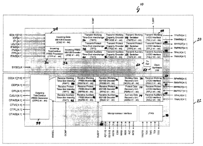
Fig. 1 is a schematic block diagram depicting an
embodiment of the bus interface.
DETAILED DESCRIPTION
Referring to Fig. 1, the bus interface 10 is depicted
having a transmit interface 20 and a receive interface 22.
5
CA 02307895 2000-OS-OS
The transmit interface 20 is comprised of an Incoming
TeleCombus PRBS Processor (ITPP) block 34, an Incoming Data
8B/10B Encoder (IDBE) block 30, an Incoming PRBS 8B/10B
Encoder (IPBE) block 32, Transmit Time-Slot Interchange
(TTSI) blocks 36, 38 and 40, Transmit 8B/10B Running
Disparity Encoder (TRDE) blocks 42, 44 and 46, Transmit
Serialiser (PISO) blocks 48, 50 and 52 and LVDS Transmitter
(TXLV) blocks 54, 56 and 58.
Incoming TeleCombus PRBS Processor
The Incoming TeleCombus PRBS Processor (ITPP) block 34
provides in-service and off-line diagnostics of the incoming
TeleCombus stream and equipment downstream of the three sets
of transmit LVDS links. Within the ITPP block 34, a total of
four ITPP sub-blocks (ITPP #1-#4) are instantiated in the
Telecom Bus Serialiser (TBS) device. Each ITPP sub-block has
the capacity to monitor and source Pseudo Random Bit Sequence
(PRBS) data of an STS-12/STM-4 stream. A set of four ITPP
blocks may be connected in tandem to service an
STS-48c/STM-16-16c stream.
The Incoming TeleCombus PRBS Processor (ITPP) block 34
includes a PRBS detector and a PRBS generator.
6
CA 02307895 2000-OS-OS
PRBS Detector
Each ITPP sub-block has an independent PRBS detector and
generator. The PRBS detector in ITPP #1 to ITPP #4 monitors
the four sections of the incoming data stream ID[1][7:0] to
ID[4][7:0], respectively. When enabled, the PRBS detector
monitors synchronous payload envelope (SPE) / higher order
virtual container (VC3 or VC4-Xc) bytes in the incoming data
stream. The incoming data is compared against the expected
value derived from an internal linear feedback shift register
(LFSR) with a polynomial of Xz' + X18 + 1. If the incoming
data fails to match the expected value for three consecutive
bytes, the PRBS detector will enter out-of-synchronization
(OOS) state. The LFSR will be re-initialized using the
incoming data bytes. The new LFSR seed is confirmed by
comparison with subsequent incoming data bytes. The PRBS
detector will exit the OOS state when the incoming data
matches the LFSR output for three consecutive bytes. The
PRBS detector will remain in the OOS state and re-load the
LFSR if confirmation failed. The PRBS detector counts PRBS
byte errors and optionally generates interrupts when it
enters and exits the OOS state.
The PRBS detector may be configured to also monitor the
B1 and E1 bytes in the incoming date stream. The B1 byte in
each incoming STS-1/STM-0 is compared with an independently
software programmable value. The E1 byte is compared with
7
CA 02307895 2000-OS-OS
the complement of the programmable value. An interrupt is
optionally generated when there is a change from the matched
to mismatched state and vice-versa. The incoming B1 bytes
are captured in a set of software readable registers. This
facility allows in-service diagnosis of provisioning errors
in upstream cross-connect devices.
PRBS Generator
The PRBS generator in ITPP #1 to ITPP #4 may optionally
overwrite the data in incoming data stream ID[1][7:0] to
ID[4][7:0], respectively. When enabled, the PRBS generator
inserts synchronous payload envelope (SPE) / higher order
virtual container (VC3 or VC4-Xc) bytes into the serial
transmit links. The inserted data is derived from an
internal linear feedback shift register (LFSR) with a
polynomial of Xz' + X1$ + 1.
The PRBS generator may be configured to optionally
insert a software programmable byte into the Bl byte of each
STS-1/STM-0 stream the serial transmit links. The E1 bytes
may be over-written to the complement of the value inserted
into the B1 bytes. This facility allows in-service
diagnosis of provisioning errors in downstream cross-connect
devices.
8
CA 02307895 2000-OS-OS
The Incoming Data 8B/lOB Encoder (IDBE) block 34
constructs an 8B/10B character stream from an incoming
TeleCombus carrying an STS-12/STM-4 stream. Within the IDBE
block 34, a total of four IDBE sub-blocks (IDBE #1 to #4) are
instantiated in the TBS device. IDBE sub-blocks #1 to #4
process incoming data streams ID[1][7:0] to ID[4][7:0],
respectively.
Each of the IDBE sub-blocks #1 to #4 of IDBE block 34
includes a frame counter and an 8B/10B encoder.
Frame Counter
The Frame Counter keeps track of the octet identity of
the incoming data stream. The Frame Counter is initialized
by the JO pulse on the IJOJ1 and IPL signals. It identifies
the positive stuff opportunity (PSO) and negative stuff
opportunity (H3) bytes within the transport frame so that
high-order path pointer justification events can be
identified and encoded.
8B/10B Encoder
The 8B/10B encoder converts bytes in the incoming
STS-12/STM-4 stream to 8B/10B characters. It can operate in
one of three modes; multiplex section termination (MST),
high-order path termination (HPT) and low-order path
9
CA 02307895 2000-OS-OS
termination (LPT) modes. The modes relate to the level of
SONET/SDH processing capability in the external device
driving the incoming TeleCombus (ID[4:1][7:0]).
In MST mode, the upstream device is a multiplex section
terminator. It has identified transport frame boundaries.
The first JO byte (JO) is encoded by an 8B/10B control
character. Incoming TeleCombus signals ITV5[4:1], ITPL(4:1],
and ITAIS[4:1] and the J1 portion of IJOJ1[4:1] are ignored.
In HPT mode, the upstream device is a high-order path
terminator. and has performed pointer processing to identify
STS/AU level pointer justification events. It has processed
all the STS/VC3/VC4 path overhead bytes. The H3 bytes in the
absence of negative pointer justification events, the PSO
byte in the presence of positive pointer justification events
may be encoded. Alternately, the J1 byte may be encoded.
Incoming TeleCombus signals ITV5[4:1], ITPL[4:1], and
ITAIS[4:1] are ignored.
In LPT mode, the upstream device is a low-order path
terminator. It has performed tributary level pointer
processing to identify tributary payload bytes and have
terminated tributary payload / low-order virtual container
bytes. In addition to MST and HPT mode bytes, V5 bytes and
all bytes that are not part of a low-order path payload are
CA 02307895 2000-OS-OS
encoded. Note that in drop-and-continue operation, the TBS
must be configured to regard the upstream device as one
appropriate for the continued path.
Table 1 shows the mapping of TeleCombus control bytes and
signals into 8B/10B control characters. The table is divided
into three sections, one for each software configurable mode
of operation.
Table 1: Serial TeleCombus 8B/10B character mapping
Code C3rouD Curr. RD- Curr. RD+ Decoded Sigaale
Name
abcdei fQhj abcdei f Dascriytion
h
Mult3 lex Mode
Section
Terminatioa
MST
K28.5 001111 1010 110000 0101 IJOJ1='b1, IPL = 'b0
Trans ort frame ali nment
K.28.4- 001111 0010 _ IPAIS='b1'
Hi h-order ath AIS
Hi h-Order ermiaatioa Mode
Path T HPT
IPL = 'b0,
K28.0- 001111 0100 - High-order path H3 byte,
no ne ative 'ustification
event
IPL = 'b0
K28.0+ - 110000 1011 High-order path positive
stuff
opportunity byte, positive
'ustification event
K28.6 001111 0110 110000 1001 IJ1='b1', IPL = 'b1
Hi h-order ath frame ali
nment
Low-Order rmiaatioa ode
Path Te LPT M
ITV5 = 'bl " ITPL = 'bl
K27.7- 110110 1000 - Low order path frame alignment
ID(0,4] = ERDI[1:0] _ 'b00,
ID[5] = REI = 'b0
ITV5 = 'bl, ITPL = 'b1
er
al
ent
e
K27.7+ - 001001 0111 b0o
-
ID[p~4a
ERDI[lrp
ID[5] = REI = 'bl
ID[7,6,3:1] _ 'b00000
ITVS = 'bl, ITPL = 'bl
er
e
al
g
nment
K28.7- 001111 1000 - =
b
O
ERDI[lr0~
ID[0~4a
ID(5] = REI = 'b0
ID[7,6,3:1] _ 'b00000
ITVS = 'bl, ITPL = 'bl
Low order path frame alignment
K28.7+ - 110000 0111 ID[0,4] = ERDI[1:0] _ 'b01,
ID[5] = REI = 'bl
ID[7,6,3:1] _ 'b00000
ITVS = 'bl, ITPL = 'bl
er
e
al
g
ent
K29.7- 101110 1000 - -
b
o
ID[0~4a
ERDI[lrp~
ID[5] = REI = 'b0
ID[7,6,3:1] _ 'b00000
ITV5 = 'bl, ITPL = 'bl
Low order path frame alignment
K29.7+ - 010001 0111 ID[0,4] = ERDI[1:0] _ 'b10,
ID[5] = REI = 'bl
ID[7,6,3:1] _ 'b00000
K30.7- 011110 1000 _ ITV5 = 'bl, ITPL = 'b1
Low order ath frame ali
nment
11
CA 02307895 2000-OS-OS
ID[0,4] = ERDI[1:0] _ 'bll,
ID[5] = REI = 'b0
ID[7,6,3:1] _ 'b00000
ITVS = 'bl, ITPL = 'bl
Low order path frame alignment
K30.7+ - 100001 0111 ID[0,4] = ERDI(1:0] _ 'b11,
ID[5] = REI = 'bl
ID[7,6,3:1] _ 'b00000
ITPL = 0
Non low-order path payload
overhead
K23.7- 111010 1000 000101 0111 bytes (RSOH, MSOH, POH,
R, V1, V2,
V3, V4)
ID[7:0] _ 'h00
ITAIS='b1'
K.28.4+ - 110000 1101 Low-order path AIS
ID[7:0] _ 'hFF
The Incoming PRBS 8B/10B Encoder (IPBE) block 32
constructs an 8B/10B character stream from the output of the
ITPP block 30. Within the IPBE block 32, a total of four
IPBE sub-blocks (IPBE #1 to #4) are instantiated in the TBS
device. IPBE sub-blocks #1 to #4 process data from ITPP sub-
blocks #1 to #4, respectively. The IPBE block 32 may be
functionally identical to the IDBE block 34.
The Transmit Time-slot Interchange (TTSI) blocks 36, 38
and 40 re-arrange the constituent STS-1/STM-0 streams of an
STS-48/STM-16 stream in a software configurable order. The
TTSI blocks 36, 38 and 40 also support multi-casting where an
incoming STS-1/STM-0 stream is placed on two or more outgoing
time-slots. The Transmit Working Time-slot Interchange
(TWTI) block 36 performs time-slot re-arrangement for data
destined for the working transmit LVDS links
12
CA 02307895 2000-OS-OS
(TPWRK[4:1]/TNWRK[4:1]). The Transmit Protection Time-slot
Interchange (TPTI) block 38 services the protection transmit
LVDS links (TPPROT[4:1]/TNPROT[4:1]) while the Transmit
Auxiliary Time-slot Interchange (TATI) block 40 services the
auxiliary transmit LVDS links (TPAUX[4:1]/TNAUX[4:1]).
Each of the TTSI blocks 36, 38 and 40 includes a Data
Buffer and Connection Memory.
Data Buffer
The Data Buffer contains a double buffer structure. The
incoming data stream is first loaded into an input shift
register. A frame counter initiates a transfer of the data
to the holding register once all 48 constituent STS-1/STM-0
streams have been shifted in. The data is read out of the
holding register in the order specified by the Connection
Memory.
Connection Memory
The Connection Memory contains two mapping pages: page
0 and page 1. One page is designated the active page and the
other the stand-by page. Selection between which page is to
be active and which is to be stand-by is controlled by the
TCMP signal. The Connection Memory samples the value on the
TCMP signal at the JO byte position of the incoming data
stream and swaps the active/standby status of the two pages
13
CA 02307895 2000-OS-OS
at the first A1 byte of the next frame. This arrangement
allows all devices in a cross-connect system to be updated in
a coordinated fashion. Consequently, STS-1/STM-0 streams not
being assigned new time-slots are unaffected by page swaps.
The Transmit 8B/10B Running Disparity Encoder (TRDE)
blocks 42, 44 and 46 correct the running disparity of an
8B/10B character stream. The input data to the TRDE blocks
42, 44 and 46 originates from either the IDBE sub-blocks #1
to #4 or the IPBE sub-blocks #1 to #4 at which point they
have correct running disparity. However, due to the
time-slot re-arrangement activities of the TTSI blocks 36, 38
and 40, the running disparity is no longer consistent. The
TRDE block inverts the 6B and 4B sub-characters to ensure
correct running disparity.
There are a total of twelve TRDE sub-blocks instantiated
in the TBS device. Four TRDE sub-blocks (TWDE #1 to #4),
within Transmit Working Disparity Encoder 42 are dedicated to
the working transmit LVDS links (TPWRK[4:1]/TNWRK[4:1]). The
Transmit Protection Disparity Encoder 44 (TPDE #1 to #4)
correct running disparity for characters destined for the
protection transmit LVDS links (TPPROT[4:1]/TNPROT[4:1])
while the Transmit Auxiliary Disparity Encoder 46 (TADS #1 to
14
CA 02307895 2000-OS-OS
#4) service the auxiliary transmit LVDS links
(TPAUX[4:1]/TNAUX[4:1]).
Transmit Serialiser
The Transmit Serialiser (PISO) blocks 48, 50 and 52
convert 8B/10B characters to bit-serial format. There are a
total of twelve PISO sub-blocks instantiated in the TBS
device. Four PISO sub-blocks, Transmit Working Serialiser 48
(TWPS #1 to #4) are dedicated to the working transmit LVDS
links (TPWRK[4:1]/TNWRK[4:1]). The Transmit Protection
Serialiser 50 (TPPS #1 to #4) generate serial streams for the
protection transmit LVDS links (TPPROT[4:1]/TNPROT[4:1])
while the Transmit Auxiliary Serialiser 52 (TAPS #1 to #4)
are associated with the auxiliary transmit LVDS links
(TPAUX[4:1]/TNAUX[4:1]).
LVD~ Transm~ tter
The LVDS Transmitters (TXLV) blocks 54, 56 and 58
convert 8B/10B encoded digital bit-serial streams to LVDS
signaling levels. A total of twelve TXLV sub-blocks are
instantiated in the TBS device. Four TXLV sub-blocks,
Transmit Working LVDS Interface 54 (TWLV #1 to #4) drive the
working transmit LVDS links (TPWRK[4:1]/TNWRK[4:1]). The
Transmit Protection LVDS Interface 56 (TPLV #1 to #4) drive
the protection transmit LVDS links (TPPROT[4:1]/TNPROT[4:1])
while the Transmit Auxiliary LVDS Interface 58 (TALV #1 to
CA 02307895 2000-OS-OS
#4) are associated with the auxiliary transmit LVDS links
(TPAUX[4:1]/TNAUX[4:1]).
The Clock Synthesis Unit (CSU) block 62 generates the
777.6 MHz clock for the transmit and receive LVDS links.
The Transmit Voltage Reference Generator block 60
generates bias voltages and currents for the LVDS
Transmitters.
The receive interface 22 is comprised of LVDS Receiver
blocks 64, 66, and 68, Data Recovery Units 70, 72 and 74,
Receive 8B/10B TeleCombus Decoders 76, 78 and 80, Receive
PRBS Monitors 82, 84 and 86, Receive Time-Slot Interchanges
88, 90 and 92, and an Outgoing TeleCombus PRBS Generator 94.
The LVDS Receiver (RXLV) blocks 64, 66 and 68 convert
LVDS signaling levels to SB/10B encoded digital bit-serial.
A total of twelve RXLV sub-blocks are instantiated in the TBS
device. Four RXLV sub-blocks, Receive Working LVDS Interface
64 (RWLV #1 to #4) connect to the working receive LVDS links
(RPWRK[4:1]/RNWRK[4:1]). The Receive Protection LVDS
Interface 66 (RPLV #1 to #4) connect to the protection
16
CA 02307895 2000-OS-OS
receive LVDS links (RPPROT[4:1]/RNPROT[4:1]) while the
Receive Auxiliary LVDS Interface 68 (RALV #1 to #4) are
associated with the auxiliary receive LVDS links
(RPAUX[4:1]/RNAUX[4:1]).
The Data Recovery Unit (DRU) blocks 70, 72 and 74
monitor the receive LVDS link for transitions to determine
the extent of bit cycles on the link. They then adjust its
internal timing to sample the link in the middle of the data
"eye". A total of twelve DRU sub-blocks are instantiated in
the TBS device. Four DRU sub-blocks, Working Data Recovery
Units 70 (WDRU #1 to #4) retrieves data from the working
receive LVDS links (RPWRK[4:1]/RNWRK[4:1]). The Protection
Data Recovery Units 72 (PDRU #1 to #4) process the protection
receive LVDS links (RPPROT[4:1]/RNPROT[4:1]) while the
Auxiliary Data Recovery Units 74 (RALV #1 to #4) are
associated with the auxiliary receive LVDS links
(RPAUX[4:1]/RNAUX[4:1]).
The DRU blocks also convert the serial into 10-bit
words. The words are constructed form ten consecutive
received bits without regard to 8B/10B character boundaries.
17
CA 02307895 2000-OS-OS
Receive 8B/10B Tele o ~ D od
The Receive 8B/lOB TeleCombus Decoder (RBTD) blocks 76,
78 and 80 frame to the receive stream to find 8B/10B
character boundaries. They also contain a FIFO to bridge
between the timing domain of the receive LVDS links and the
system clock timing domain. A total of twelve RBTD sub-
blocks are instantiated in the TBS device. Four RBTD sub-
blocks, Receiver Working 8B/10B Decoder blocks 76 (RWBD #1 to
#4) perform framing and elastic store functions on data
retrieved from the working receive LVDS links
(RPWRK[4:1]/RNWRK[4:1]). The Receive 8B/10B Decoder blocks
78 (RPBD #1 to #4) process data on the protection receive
LVDS links (RPPROT[4:1]/RNPROT[4:1]) while the Receive
Auxiliary 8B/10B Decoder blocks 80 (RABD #1 to #4) are
associated with the auxiliary receive LVDS links
(RPAUX[4:1]/RNAUX[4:1]).
Each of the RBTD sub-blocks includes a FIFO buffer, a
Frame Counter, Character Aligner, Frame Aligner and a
Character Decoder.
FIFO Buffer
The FIFO buffer provides isolation between the timing
domain of the associated receive LVDS link and that of the
system clock (SYSCLK). Data with arbitrary alignment to
8B/10B characters are written into a 10-bit by 24-word deep
18
CA 02307895 2000-OS-OS
FIFO at the link clock rate. Data is read from the FIFO at
every SYSCLK cycle.
Frame Counter
The Frame Counter keeps track of the octet identity of
the outgoing data stream. It is initialized by a delayed
version of the RJOFP signal. It identifies the positive
stuff opportunity (PSO) and negative stuff opportunity (H3)
bytes within the transport frame so that high-order path
pointer justification events can be identified and decoded.
Character Aligner
The Character Aligner locates character boundaries in
the incoming 8B/10B data stream. The framer logic may be in
one of two states, SYNC state and HUNT state. It uses the
8B/10B control character (K28.5) used to encode the SONET/SDH
JO byte to locate character boundaries and to enter the SYNC
state. It monitors the receive data stream for line code
violations (LCV). An LCV is declared when the running
disparity of the receive data is not consistent with the
previous character or the data is not one of the characters
defined in IEEE std. 802.3. Excessive LCVs are used to
transition the framer logic to the HUNT state.
Normal operation occurs when the character aligner is in
the SYNC state. 8B/10B characters are extracted from the
19
CA 02307895 2000-OS-OS
FIFO buffer using the character alignment of the K28.5
character that caused entry to the SYNC state. Mimic K28.5
characters at other alignments are ignored. The receive data
is constantly monitored for line code violations. If 5 or
more LCVs are detected in a window of 15 characters, the
character aligner transitions to the HUNT state. It will
search all possible alignments in the receive data for the
K28.5 character. In the mean time, the original character
alignment is maintained until a K28.5 character is found. At
that point, the character alignment is moved to this new
location and the character aligner transitions to the SYNC
state.
Frame Ali ner
The frame aligner monitors the data read from the FIFO
buffer for the JO byte. When the frame counter indicates the
JO byte position, a JO character is expected to be read from
the FIFO buffer. If a JO byte is read out of the FIFO buffer
at other byte positions, a JO byte error counter is
incremented. When the counter reaches a count of 3, the
frame aligner transitions to HUNT state. The next time a JO
character is read from the FIFO, the associated read address
is latched and the frame aligner transitions back to the SYNC
state. The JO byte error counter is cleared when a JO byte
is read from the FIFO at the expected position.
CA 02307895 2000-OS-OS
Character Decoder
The character decoder decodes the incoming 8B/10B
control characters into an extended set of TeleCombus control
signals. Table 2 shows the mapping of 8B/10B control
characters into TeleCombus control signals. The table is
divided into three sections, one for each mode of operation
(MST, HPT and LPT) in the 8B/10B encoder in an external
device upstream of the TBS. The character decoder itself is
not mode sensitive.
Table 2: Serial TeleCombus 8B/10B character decoding
Code Group Curr. RD Curr. RD+ Decoded Signals
Name ~
abcdei f cdai fQhi Description
Mul_ti lax n TesminatioaMode
Sectio MST
OJO='bl'
K28.5 001111 0100110000 1011 Transport frame alignment
OD[7:0] _ 'h01
OPAIS='bl'
K.28.4- 001111 0010- High-order path AIS
OD[7:0] _ 'hFF
8i h-Order ermination mode
Path T HPT
OPL = 'b0,
K28.0- 001111 0100_ High-order path H3 byte,
no negative justification
event
OD[7:0] _ 'h00
OPL = 'b0
K28.0+ - 110000 1011 High-order path PSO b te,
y positive
justification event
OD[7:0] _ 'h00
OJl='b1'
K28.6 001111 0110110000 1001 High-order path frame alignment
OD[7:0] _ 'h00
Lom-Order rmination ode
Path Te LPT M
OTVS = 'bl" OTPL = 'bl
K27.7- 110110 1000_ Low order path frame alignment
OD[0,4] = ERDI[1:0] _ 'b00,
OD[5] _
REI = 'b0
OTVS = 'bl, OTPL = 'bl
Low order path frame alignment
K27.7+ - 001001 0111 OD[0,4] = ERDI[1:0] _ 'b00,
OD[5] _
REI = 'bl
OD[7,6,3:1] _ 'b00000
OTV5 = 'b1, OTPL = 'b1
Low order path frame alignment
K28.7- 001111 1000- OD[0,4] = ERDI[1:0] _ 'b01,
OD[5] _
REI = 'b0
OD[7,6,3:1] _ 'b00000
OTV5 = 'bl, OTPL = 'bl
Low order path frame alignment
K28.7+ - 110000 0111 OD[0,4] = ERDI[1:0] _ 'b01,
OD[5] _
REI = 'bl
oD[7,6,3:1] _ 'booooo
K29.7- 101110 1000_ OTVS = 'b1, OTPL = 'bl
Low order ath frame ali
nment
21
CA 02307895 2000-OS-OS
OD[0,4] = ERDI[1:0] _ 'b10,
OD[5] _
REI = 'b0
OD[7,6,3:1] _ 'b00000
OTVS = 'bl, OTPL = 'bl
Low order path frame alignment
K29.7+ - 010001 0111 OD[0,4] = ERDI[1:0] _ 'b10,
OD[5] _
REI = 'bl
OD[7,6,3:1] _ 'b00000
OTV5 = 'bl, OTPL = 'b1
Low order path frame alignment
K30.7- 011110 1000 - OD[0,4] = ERDI[1:0] _ 'bll,
OD[5] _
REI = 'b0
OD[7,6,3:1] _ 'b00000
OTV5 = 'b1, OTPL = 'bl
Low order path frame alignment
K30.7+ - 100001 0111 OD[0,4] = ERDI[1:0] _ 'b11,
OD[5] _
REI = 'bl
OD[7,6,3:1] _ 'b00000
OTPL = 0
K23.7- 111010 1000 - Non low-order path payload
bytes
(RSOH, MSOH, POH, R, V1,
V2, V3, V4)
OD[7:0] _ 'h00
OTAIS='b1'
K.28.4+ - 110000 1101 Low-order path AIS
OD(7:0] _ 'hFF
The Receive PRBS Monitor (RPRM) blocks 82, 84 and 86
provide in-service and off-line diagnostics of the receive
LVDS links. A total of twelve RPRM sub-blocks are
instantiated in the TBS device. Four RPRM sub-blocks,
Receive Working PRBS Monitor 82 (RWPM #1 to #4) connect to
the working receive LVDS links (RPWRK[4:1]/RNWRK[4:1]). The
Receive Protection PRBS Monitor 84 (RPPM #1 to #4) connect to
the protection receive LVDS links (RPPROT[4:1]/RNPROT[4:1])
while the Receive Auxiliary PRBS Monitor 86 (RAPM #1 to #4)
are associated with the auxiliary receive LVDS links
(RPAUX[4:1]/RNAUX[4:1]). The RPRM blocks 82, 84 and 86 are
functionally identical to the monitor section of the ITPP
block 30.
22
CA 02307895 2000-OS-OS
Receive Time-slot Interchange
The Receive Time-slot Interchange (RTSI) blocks 88, 90
and 92 re-arrange the constituent STS-1/STM-0 streams of an
STS-48/STM-16 stream in a software configurable order. The
RTSI blocks 88, 90 and 92 also support multi-casting where a
STS-1/STM-0 stream from one of the three receive LVDS links
is placed on two or more outgoing time-slots. The Receive
Working Time-slot Interchange (RWTI) block 88 performs
time-slot re-arrangement for data sourced from the working
receive LVDS links (RPWRK[4:1]/RNWRK[4:1]). The Received
Protection Time-slot Interchange (RPTI) block 90 services the
protection receive LVDS links (RPPROT[4:1]/RNPROT[4:1]) while
the Receive Auxiliary Time-slot Interchange (RATI) block 92
services the auxiliary receive LVDS links
(RPAUX[4:1]/RNAUX[4:1]).
Ot?tao~ na P1 Pc~o ~ PRB~ n a or
The Outgoing TeleCombus PRBS Generator (OTPG) block 94
optionally inserts PRBS pattern on a per STS-1/STM-0 onto the
Outgoing TeleCombus stream. A total of four OTPG sub-blocks
(OTPG #1 to #4) are instantiated in the TBS device. Each
OTPG sub-block has the capacity to source PRBS data of an
STS-12/STM-4 stream. A set of four OTPG sub-blocks may be
connected in tandem to service an STS-48c/STM-16-16c stream.
23
CA 02307895 2000-OS-OS
The OTPG block 94 is functionally identical to the generator
section of the ITPP block 30.
LVDS Overview
The LVDS family of cells allow the implementation of
777.6 Mb/s LVDS links. A reference clock of 77.76MHz is
required. Four 777.6 Mb/s LVDS form a set of high-speed
serial data links for passing an STS-48 aggregate data
stream.
The transmitter drives a differential signal through a
pair of 5052 characteristic interconnects, such as board
traces, backplane traces, or short lengths of cable. The
receiver presents a 10052 differential termination impedance
to terminate the lines. Included in the standard is
sufficient common-mode range for the receiver to accommodate
as much as 925mV of common-mode ground difference.
Complete SERDES transceiver functionality is provided.
Ten-bit parallel data is sampled by the line rate divided-by-
10 clock (77.76MHz SYSCLK) and then serialized at the line
rate on the LVDS output pins by a 777.6MHz clock synthesized
from SYSCLK. Serial line rate LVDS data is sampled and de-
serialized to 10-bit parallel data. Parallel output
transfers are synchronized to a gated line rate divided-by-10
24
CA 02307895 2000-OS-OS
clock. The 10-bit data is passed to an 8B/10B decoding
block. The gating duty cycle is adjusted such that the
throughput of the parallel interface equals the receive input
data rate (Line Rate +/- 100ppm). It is expected that the
clock source of the transmitter and the receiver the same to
ensure that the data throughput at both ends of the link are
identical.
Data must contain sufficient transition density to allow
reliable operation of the data recovery units. 8B/10B block
coding and decoding is provided by the TBTE and RBTD blocks.
At the system level, reliable operation will be obtained if
proper signal integrity is maintained through the signal path
and the receiver requirements are respected. Namely, a worst
case eye opening of 0.7UI and 100mV differential amplitude is
needed. These conditions should be achievable with a system
architecture consisting of board traces, two sets of
backplane connectors and up to 1m of backplane interconnects.
This assumes proper design of 10052 differential lines and
minimization of discontinuities in the signal path. Due to
power constraints, the output differential amplitude is
approximately 350mV.
The LVDS system is comprised of the LVDS Receivers
(RXLV) 64, 66 and 68, LVDS Transmitter (TXLV) 54, 56 and 58,
Transmitter reference (TXREF) 60, data recovery units (DRU)
CA 02307895 2000-OS-OS
70, 72 and 74, parallel to serial converters (PISO) 48, 50
and 52 and Clock Synthesis Unit (CSU) 62.
Microprocessor Interface
The Microprocessor Interface block 98 provides normal
and test mode registers, and logic required to connect to the
microprocessor interface. The normal mode registers are
required for normal operation, and test mode registers are
used to enhance testability of the TBS.
A ~ anm n in a Mu1 t~ -de~>; rP Environ_men
The RJOFP frame pulse is used to synchronize a set of
devices that are inter-connected via LVDS links. It is
provided concurrently to all the devices in the system once
every 125~.zs, or multiples thereof. Characters retrieved from
the receive LVDS links are written into a FIFO buffer. When
the JO character is received, it is written into a fixed
location in the FIFO. Subsequent characters are written the
locations following. At each device in the system, a
software configurable counter is used to mark the point,
relative to RJOFP, where all its receive LVDS links are
expected to have delivered their JO character. As directed
by the delay counter, the device will then read the fixed
location where the JO character is stored, thus synchronizing
all the receive LVDS links. Differential delays between and
clock instabilities of LVDS links are absorbed by the FIFOs.
26
CA 02307895 2000-OS-OS
This invention provides a new use of 8b/10b control
characters to label SONET/SDH transport frame, high-order
path frame, and low-order path frame boundaries. The types
of bytes that are encoded in Sb/10b control characters are
configurable to suite different classes of SONET/SDH
equipment (multiplex section terminators, high-order path
terminators and low-order path terminators).
Furthermore, the use of 8b/10b encoding on de-scrambled
SONET/SDH data stream in order ensures data transitions on
the serial links and preserves DC balance.
The standard 8b/lOb control character set is extended by
treating the positive and negative running disparity codes of
those control characters with an even number of ones and
zeros as two separate control characters. This
implementation doubles the number of control characters
available for encoding of events. Further, DC balance is
retained without having to alternately send positive and
negative running disparity codes.
The use of FIFOs and a universal frame pulse with software
programmable delay advantageously allow the transfer of a
single SONET OC-N / SDH STM-M signal over multiple links.
27
CA 02307895 2000-OS-OS
This invention also provides a transparent in-band error
reporting facility where errors detected at the SONET/SDH
receiver can be transferred to the transmitter to construct
remote error and defect indication codes.
The occurrence of line code violations of 8b/10b
characters can be used to monitor error performance of the
serial links.
This invention further provides for PRBS pattern
insertion and monitoring thereby allowing datapath
verification prior to injection of the actual payload.
ALTERNATE EMBODIMENTS
An alternate embodiment utilizes out-of-band signaling
to mark frame boundaries, status information and alarm
events. SONET/SDH data bytes are carried in byte serial
format on a set of four 8-bit buses (ID[4:1][7:0] and
OD[4:1][7:0]). Transport frame boundaries and payload frame
boundaries are marked by the IJOJ1[4:1] and OJOJ1[4:1]
signals. SONET/SDH transport overhead bytes are
distinguished from high-order path payload bytes by the
IPL[4:1] and OPL[4:1] signals. Low order path payload
boundaries are indicated by the ITV5[4:1] and OTVS[4:1]
signals. Low-order path transport overhead bytes are
distinguished from low-order path payload bytes by the
28
CA 02307895 2000-OS-OS
ITPL[4:1] and OTPL[4:1] signals. Status and alarms are
carried by the signals IPAIS[4:1], OPAIS[4:1], ITAIS[4:1] and
OTAIS[4:1] .
The above-described embodiments should be regarded as
illustrative rather than restrictive, and it should be
appreciated that variations may be made other than those
discussed, by workers of ordinary skill in the art without
departing from the scope of the present invention.
29