Note: Descriptions are shown in the official language in which they were submitted.
CA 02307922 2000-OS-09
TITLE: SURFACE-MOUNT ELECTRICAL CONNECTION DEVICE
FIELD OF THE INVENTION
The present invention relates to the field of electrical
connectors, particularly connectors capable of being surface-
mounted to a PCB (Printed Circuit Board). More specifically,
the invention relates to an electrical connection device
including a plurality of terminal members held in a
predetermined spacial relationship that can be surface-
mounted to a PCB. The invention also extends to a method for
mounting an electrical connection device on a circuit board
and to a circuit board including such electrical connection
device.
BACKGROUND OF THE INVENTION
With the advancement of circuit board assembly has come
a technique known as surface-mount technology, which consists
in the mounting of electronic circuit components and their
electrical connections on the surface (through solder-
anchoring) of a Printed Circuit Board (PCB), rather than
through holes (also called "vias"). The PCB itself is a flat
board whose front contains slots for integrated circuit chips
and connections for a variety of electrical components, and
whose back is printed with electrically conductive pathways
between the components. An example of such an electrical
component is the electrical connector which, when mounted on
the PCB, creates an interface between discrete wires and the
PCB. Automation of the circuit board assembly process
typically involves the use of automated pick-and-place
1
CA 02307922 2000-OS-09
machinery for placement of the electrical components onto the
PCB.
Existing de-plugable type electrical connections are
usually created on the PCB in the form of surface-mount pins.
These pins are built and sold separately, each individually
surface-mounted onto the PCB by the pick-and-place machinery.
Unfortunately, due to the individual mounting of these
surface-mount pins, the accuracy of the distance between each
pin on the PCB depends entirely on the accuracy of the pick-
and-place machine. If the pins are not precisely positioned
with relation to one another on the PCB, it may be difficult,
even impossible, for the mating electrical component to
engage the pins of the electrical connection.
The background information herein clearly shows that
there exists a need in the industry to provide an improved
electrical connection device for a circuit board.
SUMMARY OF THE INVENTION
As embodied and broadly described herein, the invention
provides an electrical connection device for receiving a
mating electrical component, said electrical connection
device comprising:
- a body;
- at least two elongated terminal members mated to
said body, each terminal member including:
i) a retaining surface for establishing an
electrical contact with a circuit board, said
retaining surface capable of being solder
2
CA 02307922 2000-OS-09
anchored to the circuit board for fixing the
terminal member on the circuit board, the
retaining surfaces of the terminal members
being coplanar;
ii) a contact portion for engaging a mating
electrical terminal member of the electrical
component when the electrical component is
mounted to the electrical connection device,
the contact portions of the terminal members
l0 being substantially parallel with one another;
iii) said body maintaining said terminal members in
a predetermined spatial relationship.
The electrical connection device provides for an
accurate inter-terminal member spacing once solder-anchored
to the circuit board. Further, an electrical connection
device including multiple terminal members may be placed on
the circuit board in a single step. Thus, the automation of
the surface-mount assembly operation is greatly simplified.
As embodied and broadly described herein the invention
also provides a method for mounting an electrical connection
device on a circuit board, said electrical connection device
comprising:
- a body;
- at least two elongated terminal members mated to
said body, each terminal member including:
i) a retaining surface for establishing an
electrical contact with a circuit board, said
retaining surface capable of being solder-
anchored to the circuit board for fixing the
3
CA 02307922 2000-OS-09
terminal member on the circuit board, the
retaining surfaces of the terminal members
being coplanar;
ii) a contact portion for engaging a mating
electrical terminal member of the electrical
component when the electrical component is
mounted to the electrical connection device,
the contact portions of the terminal members
being substantially parallel with one another;
iii) said body maintaining said terminal members in
a predetermined spatial relationship;
- said method comprising the steps of:
i) positioning the electrical connection device
on said circuit board such that the retaining
surfaces of said terminal members are aligned
with solder pads on the circuit board;
ii) soldering said retaining surfaces to the
circuit board.
As embodied and broadly described herein the invention
further provides a circuit board comprising:
- a substrate layer;
- a plurality of contact pads mounted to said
substrate layer;
- an electrical connection device for receiving a
mating electrical component, said electrical
connection device comprising:
i) a body;
4
CA 02307922 2000-OS-09
ii) at least two elongated terminal members mated
to said body, each terminal member including:
a) a retaining surface for establishing an
electrical contact with the circuit
board, said retaining surface capable of
being solder-anchored to one of said
contact pads for fixing the terminal
member on the circuit board, the
retaining surfaces of the terminal
members being coplanar;
b) a contact portion for engaging a mating
electrical terminal member of the
electrical component when the electrical
component is mounted to the electrical
connection device, the contact portions
of the terminal members being
substantially parallel with one another;
c) said body maintaining said terminal
members in a predetermined spatial
relationship.
BRIEF DESCRIPTION OF THE DRAWINGS
These and other features of the present invention will
become apparent from the following detailed description
considered in connection with the accompanying drawings. It
is to be understood, however, that the drawings are provided
for purposes of illustration only and not as a definition of
the boundaries of the invention, for which reference should
be made to the appending claims.
5
CA 02307922 2000-OS-09
Figure 1 is a perspective exploded view of a surface-
mount, electrical connection device, in accordance with an
embodiment of the present invention;
Figure 2 is an assembled view of the surface-mount,
electrical connection device shown in Figure l, shown in
position to be mounted on a PCB;
Figure 3 is a side-view of the surface-mounted
electrical connection device shown in Figure 2, shown in
position to connect to a de-plugable electrical connector.
DESCRIPTION OF A PREFERRED EMBODIMENT
In a most preferred embodiment, the electrical
connection device to be surface-mounted on a PCB is as shown
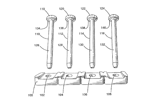
in Figure 1. The body 100 of the electrical connection
device is a strip of insulating material, such as plastic,
and is molded to include a plurality of apertures. Specific
to this example, the body 100 (also referred to as molded
strip) includes apertures 102, 104, 106 and 108. The
electrical connection device further includes terminal
members 110, 112, 114 and 116, themselves including end
surfaces 118, 120, 122 and 124, respectively, and contact
portions 126, 128, 130 and 132, respectively. Specific to
this example, terminal members 110, 112, 114 and 116 are male
contact pins. The end surfaces, hereinafter referred to as
retaining surfaces, serve as points of both solder-anchoring
and electrical contact between the electrical connection
device and the PCB, and will be described from a functional
point of view in further detail below. The contact portions
serve as points of electrical contact between the PCB and an
electrical component, such as a mating de-plugable electrical
connector, as well as provide for the removable mounting of a
6
CA 02307922 2000-OS-09
de-plugable electrical component to the PCB. This latter
functionality of the contact portions will also be described
in further detail below.
Each pin includes a head having a radially outwardly
projecting shoulder, where this head forms, at least in part,
a flange-shaped retaining surface. The contact portion
extends from the head, in a direction normal to the radial
plane of the head. The contact portion of the pin is
cylindrical, with a constant diameter along most of its
length. Apertures 102, 104, 106 and 108 are matched in
diameter to the diameter of the plug portions 126, 128, 130
and 132, for ensuring a tight friction fit of the pins 110,
112, 114 and 116 in the molded strip 100.
Figure 2 illustrates the assembled electrical connection
device, ready for surface-mounting to a PCB 200. The PCB 200
may include multiple integrated circuit chips and connections
for a variety of other electrical components, none of which
are shown in Figure 2 in the interest of clarity. The PCB
200 further includes a plurality of solder pads for securely
mounting the electrical connection device to the PCB 200.
Solder pads 202, 204, 206 and 208 are matched in size, shape
and spacing with retaining surfaces 118, 120, 122 and 124,
respectively, and serve as points of both electrical contact
and anchoring between the electrical connection device and
the PCB 200, once soldered with the pins.
In Figure 3, the surface-mounted electrical connection
device is in position for engaging a mating de-plugable
electrical connector 300 to the PCB 200. Seen from the side,
pin 110 is positionally matched to a mating terminal member
of the connector 300, specifically aperture 302. Although
not shown in Figure 3, the connector 300 also includes three
other apertures for receiving pins 112, 114 and 116. The
7
CA 02307922 2000-OS-09
circular cross-section diameter of the cylindrical pins 110,
112, 114 and 116 is such that the pins fit tightly into the
connector 300 apertures. The apertures include contact
members that touch the pins when the electrical connection
device is mated to the connector 300. In turn, those contact
members may lead to wires (not shown in the drawings).
In use, the molded strip 100 is fitted with the pins
110, 112, 114 and 116, whereby contact portions 126, 128, 130
and 132 are pressed into apertures 102, 104, 106 and 108,
respectively, of the molded strip 100. The dimension
matching between pins and apertures ensures that once the
pins are fitted into the apertures, they are tightly retained
in place by friction forces. The pins are fitted into the
apertures of the molded strip 100 such that the clearance
distance D (shown in Figure 3) between the lower edges 134,
136, 138 and 140 of the retaining surfaces 118, 120, 122 and
124 and the molded strip 100 is substantially the same for
all four pins. This ensures that the retaining surfaces are
all co-planar, necessary for an even soldering between the
connection device and the PCB 200. The clearance distance D
facilitates soldering of the electrical connection device to
the PCB 200.
The assembled electrical connection device is next
placed on the PCB 200, positioned such that the retaining
surfaces 118, 120, 122 and 124 are aligned with solder pads
202, 204, 206 and 208, respectively. The placement of the
electrical connection device, including all four pins, onto
the PCB 200 may be performed in a single step by pick-and-
place machinery in an automated assembly operation. This is
an important advantage over existing surface-mount, de-
plugable type connections, where separate pins are
8
CA 02307922 2000-OS-09
individually placed and surface-mounted onto the PCB,
requiring multiple steps.
In an alternative embodiment of the present invention,
the electrical connection device may include a pick-and-place
pad for easing the assembly of the electrical connection
device to the PCB 200 as performed by the pick-and-place
machinery. In a specific example, this pad may take the form
of a second molded strip installed on all or a subset of the
pins (at the opposite end from the retaining surfaces), for
increasing the surface area available to the pick-and-place
machinery for picking up the electrical connection device.
Once the device is mounted on the PCB 200, the pick-and-place
pad may be removed.
Once properly placed on the PCB 200, the electrical
connection device retaining surfaces 118, 120, 122 and 124
are soldered to the PCB 200. The retaining surfaces 118,
120, 122 and 124 of the pins are thin enough to allow for
quick heating to soldering temperatures. As such a
characteristic is common to typical solder contacts and is
well known to those skilled in the art, it will not be
described in further detail. Since all retaining surfaces
are co-planar, an even soldering between the electrical
connection device and the PCB 200 is assured. The molded
strip 100 ensures an accurate spacing between pins 102, 104,
106 and 108, such that no discrepancies arise between the
inter-pin spacing on the electrical connection device and the
inter-solder pad spacing on the PCB 200. This feature also
insures that once soldered, the pins of the electrical
connection device will precisely mate with the apertures of
the electrical connector 300. Note that once the electrical
connection device has been secured (soldered) to the PCB 200,
the molded strip 100 can be removed by pulling it off of the
9
CA 02307922 2000-OS-09
pins. This will allow the connector 300 to lay flush against
the PCB 200 once it is mated to the pins of the electrical
connection device, as required by certain low profile
electrical components.
The surface-mounted connection device may now be used to
removably mount a de-plugable electrical component to the PCB
200. As shown in Figure 3, a de-plugable connector 300 is
positioned such that its apertures are aligned with the
contact portions 126, 128, 130 and 132 of pins 102, 104, 106
and 108. An external force applied to the de-plugable
connector 300 can push the connector 300 onto the PCB 200
such that the contact portions 126, 128, 130 and 132 of the
surface-mounted connection device tightly plug the connector
300 apertures. When the connector 300 is to be serviced
outside of the PCB 200, it may be pulled off of the PCB 200,
the connector 300 apertures gradually releasing the
electrical connection device pins 102, 104, 106 and 108.
The above description of a preferred embodiment under
the present invention should not be read in a limitative
manner as refinements and variations are possible without
departing from the spirit of the invention. The scope of the
invention is defined in the appended claims and their
equivalents.