Note: Descriptions are shown in the official language in which they were submitted.
CA 02308000 2000-OS-10
INFRARED TRANSCEIVER ASSEMBLY FOR ASYMMETRIC DATA
TRANSMISSION
Technical Field of the Invention
This invention relates to optoelectronic transceivers used in optical
communication
systems, and more specifically to an optical transceiver configured for
transmission and
reception of infrared optical signals within an asymmetrically shaped optical
profile.
Background of the Invention
Some previous optical transceivers used optical profiles that were uniform or
broad.
Some previous transceivers used narrow optical profiles by using emitter and
receiver lenses
oriented in different angles aimed in different directions in relation to each
other to reduce
optical signal interference to improve communication. However, this increased
manufacturing
costs and the size of the transceiver package, as well as limiting utility.
The Infrared Data Association (IrDA) published a standard titled Infrared Data
Association Serial Infrared Physical Layer Specification (V 1.3, 1 S October
1998) which
contained the Advanced Infrared (Alr) communications standard. This standard
defines a
physical link layer protocol having infrared (IR) detectors, such as a
photodetector for detecting
received infrared light, and an emitter, such as a light emitting diode (LED)
for emitting light up
to a transfer rate of 4 Mb/s within a predetermined asymetrically-shaped
optical profile having
orthogonal minor and major axes with concentric centres. Along the major axis,
the half power
level of the profile shape is located at the outward edges of a cone which
subtends an angle of 60
degrees that straddles a line normal to the major axis, and along the minor
axis, the half power
level of the profile shape is located at the outward edges of a cone which
subtends an angle of 15
degrees that straddles a line normal to the minor axis. The shape of the
optical profile is designed
to maximize the 'reach space' along a direction orthogonal to the major axis,
and minimize the
'reach space' along a direction orthogonal to the minor axis. It was
originally conceived that the
major axis would be aligned in a horizontal direction relative to a floor
surface so that optical
communications could occur within a collaborative workplace environment.
CA9-1999-0027 1
CA 02308000 2000-OS-10
Prior art optical transceivers have a photodetector and an LED positioned
adjacent to
each other on the same plane using dedicated lenses or surfaces disposed over
the photodetector
and the LED. The lenses typically had a circular-shaped outer perimeter. A
problem with prior
art devices when using a photodetector is excessive Link Turn Around Time
(LTAT) which
slows the communications. An LED can transmit enough light or optical rays to
saturate an
adjacent photodetector, thus rendering the photodetector temporarily unable to
receive optical
rays. The saturated photodetector requires a predetermined amount of time
(i.e., LTAT) to
recover and become normalized enough to then be ready to reliably detect
incoming optical rays.
With prior art configurations, the communication process was required to wait
for the saturated
photodetector to normalize each time the adjacent LED completed a transmission
cycle. A
familiar example of a saturated optical sensor is a human eye that is exposed
to too much light.
This causes the retina to become temporarily blinded (i.e., saturated). Before
the eye can once
again detect images, the eye must normalize during a recovery time after the
light is removed.
Therefore, it is desirable to find a solution to overcome the problem of
optically
isolating the photodetector from the LED to avoid saturating the photodetector
when the LED is
adjacent to the photodetector for maintaining continued communication by
eliminating the wait
or idle time while the photodetector normalizes. Some prior art methods
addressed this by
interposing a physical barrier between the photodetector and the LED to block
light or optical
rays from leaving the LED and reaching the photodetector. However, this causes
a transceiver to
become larger and more complicated. This is undesirable for portable computers
or small-sized
computing devices like laptop computers or hand-held personal digital devices
which require an
optical transceiver of a small size or form factor. Therefore, another
objective of this invention is
to configure a transceiver having a small physical size for use in portable
computing devices and
the like.
Maurin et al in US patent 5,811,798 Sealed Photoelectric Detector dated 22
September
1998, along with Isaksson in WO patent 09201 6021A Optoelectronic Component
dated 27
February 1991, discloses using a solid barrier that is interposed between the
transmitter (emitter)
and receiver (photodetector) for preventing the transmitter from radiating
light or optical rays
into the adjacent receiver when using the transceiver in free-space condition.
Apparently, there is
CA9-1999-0027 2
CA 02308000 2000-OS-10
no concern or regard to the overall physical size of the transceiver which is
an important issue if
the transceiver is to be used with small-sized electronic systems nor the
optical profile.
Johnson et al in US patent 5,359,446 Wide-angle, High-speed, Free-space
Optical
Communications System dated 25 October 1994 discloses using an interposing
solid barner for
S preventing a transmitter (emitter) from radiating light into an adjacent
receiver (photodetector).
This appears to be designed for a limited-space condition that is isolated
from true free space by
a shroud in order to achieve full duplex mode communications in which the
receiver and the
adjacent transmitter operate simultaneously or asynchronously. It does not
address optical
profiles nor appear to be capable of operation in free field conditions. It
appears that the
asynchronous communication occurs in a limited space within the boundaries of
an opaque
shroud, and does not occur within true free space or unrestricted space.
Rosenberg in US patent 5,506,445 Optical Transceiver Module dated 9 April 1996
discloses a structure for an ordinary optical transceiver, and does not
disclose a structure that can
satisfy the Alr communications standard.
1 S The above listed prior art does not suggest how to prevent degrading a
transceiver's
communication performance while satisfying limitations on size for use with a
portable PC,
especially when the transceiver communicates within an asymmetrically shaped
optical profile.
The transceiver's communication ability may be degraded by several factors
that are not
addressed in combination by the prior art, such as:
(a) optical rays from an LED lens that enters into the photodetector lens
because of the
relative positions of the lenses with respect to each other;
(b) an LED saturating an adjacent photodetector that causes communication
delays; and
(c) a photodetector lens that partially blocks the optical rays emitting from
the LED lens
thus creating a shadow that blocks optical rays being emitted from the LED.
To overcome these problems, the lenses could be separated further apart to
keep the
profiles of the emitter (LED) and receiver lenses from interfering with each
other; however, the
transceiver size will then be larger and thus less desirable for use in a
portable PC.
Therefore, a solution should address, balance, and satisfy several technical
problems in
combination, such as:
CA9-1999-0027 3
CA 02308000 2000-OS-10
(a) isolating the specific optical profiles for optimum condition of
transmission and
reception of optical rays;
(b) preventing a photodetector from becoming saturated by an adjacent LED,
thus not
allowing the communication process to idle unnecessarily;
(c) minimizing the transceiver's package size; and
(d) communicating optical rays freely within the specified optical profiles.
The prior art does not suggest a solution for simultaneously addressing the
above-mentioned problems in combination.
A lens may be used with an emitter (such as an LED) and a detector (such as a
photodetector) to define the shape of the optical profile of light being
emitted from or received
by those devices. The profile resembles a spatial conduit having a non-
contact, non-reflecting
boundary in which the optical rays of communication are spatially confined
while being directed
to and from the emitter and detector. This spatial conduit is also called the
Field-of View (FOV).
Asymmetrically shaped optical profiles were not used by computers (PCs)
communicating with
each other in prior art. The Alr communications standard requires the
photodetector to receive
optical rays and the LED to transmit optical rays within the asymmetrically
shaped profile.
As will be known by those skilled in the art, an optical profile represents a
spatial
pathway having defined spatial boundaries which can advantageously be useful
for optical
communications. For example, a flashlight having an internal reflector
outwardly projects a
cone-shaped light beam or profile, and the space inside the cone has a density
of light rays while
the space outside the cone the density of light rays is much less. In reality,
the transition from
one region to the other is not abrupt, but rather assumes a Gaussian-shaped
transition.
Summary of the Invention
The present invention addresses the problems related with shadows that are
created by
adjacently located lenses, and saturation of the photodetector, while
providing an optical
transceiver configured for applications that demand a very small package size
or form factor, and
providing fast, reliable communication within an asymmetrically shaped optical
profile.
One aspect of the present invention provides a transceiver having lenses
positioned and
aligned to allow the transceiver to be placed in a small-sized package, while
giving the
CA9-1999-0027 4
CA 02308000 2000-OS-10
advantageous optical responsiveness for use in a limited space or footprint
within computing or
communication platforms, where the transceiver typically operates in half
duplex mode, while
maintaining capability to operate -- without requiring further physical
modifications -- in
communication systems that operate in full duplex mode.
Another aspect of the present invention provides an optical transceiver that
communicates within an asymmetrically shaped optical profile by using
ellipsoidally-shaped
lenses. The emitter and receiver lenses are spatially positioned with their
major axes staggered so
that the optical profiles of lenses do not optically interfere with each
other.
Yet another aspect of the present invention provides a transceiver for
receiving and
transmitting optical signals within an asymmetrically shaped optical profile
including:
(a) an emitter group having at least one emitter module, the emitter module
having:
(i) at least one emitter element for emitting an output optical signal in
response to
an output electrical signal;
(ii) an emitter lens element having orthogonal major and minor axes disposed
in
relation to the emitter element to confine light emitted from the emitter
element within the profile;
(b) a receiver group having at least one receiver module, the receiver module
having:
(i) at least one receiver element for producing an input electrical signal in
response to receiving an input optical signal;
(ii) a receiver lens element having orthogonal major and minor axes disposed
in
relation to the receiver element to confine light received by the receiver
lens
within the profile onto the receiver element;
(c) the emitter and receiver modules disposed on the transceiver in staggered
parallel
spaced relation to each other with respect to their minor axes.
Another aspect of the present invention provides a transceiver in which:
(a) the emitter group includes a number of spaced emitter modules aligned in a
column
along their minor axes;
(b) the receiver group includes a number of spaced receiving modules aligned
in a
column along their minor axes;
CA9-1999-0027 5
CA 02308000 2000-OS-10
(c) the columns of the modules are disposed in parallel spaced relationship
with each
other; and
(d) the emitter modules are staggered with respect to the receiver modules in
their
respective columns.
Yet another aspect of the present invention provides a transceiver in which:
(a) the emitter group includes two spaced emitter modules aligned in a column
along
their minor axes, and the receiver group includes one receiver module; and
(b) the receiver module is staggered with respect to the emitter modules and
offset
therebetween.
Still another aspect of the present invention provides a communication system
for
receiving and transmitting optical signals within an asymmetrically shaped
optical profile
including:
(a) an emitter group having at least one emitter module, the emitter module
including:
(i) at least one emitter element for emitting an output optical signal in
response to
an output electrical signal;
(ii) an emitter lens element having orthogonal major and minor axes disposed
in
relation to the emitter element to confine light emitted from the emitter
element within the profile;
(b) a receiver group having at least one receiver module, the receiver module
including:
(i) at least one receiver element for producing an input electrical signal in
response to receiving an input optical signal;
(ii) a receiver lens element having orthogonal major and minor axes disposed
in
relation to the receiver element to confine light received by the lens within
the
profile onto the receiver element;
(c) the emitter and receiver modules are disposed on the transceiver in
staggered parallel
spaced relation to each other with respect to their minor axes.
Preferably, the present invention can be configured so that the asymmetrically
shaped
profile has an oblong shape when viewed in a plane parallel to the major and
minor axes of the
lenses, the oblong shape having an oblong major axis corresponding to the
major axes of the
lenses, and an oblong minor axis corresponding to the minor axes of the
lenses.
CA9-1999-0027 6
CA 02308000 2000-OS-10
Brief Description of the Drawings of the Invention
The invention will now be further described by way of example only and with
reference
to the following drawings wherein:
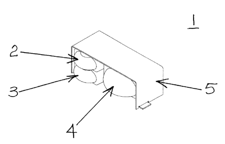
Fig. l shows a perspective of an embodiment of the present invention in which
the lenses
S are spatially positioned to minimize the transceiver's size while maximizing
communication
performance;
Fig.2 shows a front view of the embodiment of the present invention;
Fig.3 shows a side view of the first embodiment of the present invention
detailing a side
view of the stacked arrangement of the transmission lenses along the vertical
direction;
Fig.4 shows another side view of the first embodiment of the present invention
detailing
a side view of the receiving lens and photodetector;
Fig.S shows a frontal side view of the embodiment of the present invention;
Fig.6 shows a cross section of the optical power distribution along the major
and minor
axes of the lenses;
Fig.7 shows a cross sectional perspective of the emitter lens along the major
axis;
Fig.8 shows a cross sectional perspective of the emitter lens along the minor
axis;
Fig.9 shows a cross sectional perspective of the receiver lens along the major
axis;
Fig.10 shows a cross sectional perspective of the receiver lens along the
minor axis.
Detailed Description of the Preferred Embodiment
Fig. l shows a perspective view of a preferred embodiment of the present
invention. This
embodiment comprises an optical transceiver ( 1 ) which has a housing (5) and
includes a first
emitter lens (2) and a second emitter lens (3) each having minor axes in-line
and spaced apart in
one direction, such as in a vertical direction, and also has major axes along
an orthogonal
direction, such as in a horizontal direction. The transceiver ( 1 ) further
includes a receiver lens (4)
having its major axis parallel with the horizontal direction and its minor
axis aligned along the
vertical direction, and the major axis of the receiver lens (4) is spatially
positioned equidistantly
between the major axes of the emitter lenses (2, 3) while the minor axis of
the receiver lens (4) is
spaced apart from the minor axes of the emitter lenses (2, 3) for positioning
the lenses (2, 3, 4) in
a horizontally alternating manner so that the housing (5) of the optical
transceiver (1) has a very
CA9-1999-0027 7
CA 02308000 2000-OS-10
small size without causing interference (shadowing) between the emitter and
receiver lenses. The
lenses (2, 3, 4) are contained within the housing (5). The emitter lenses (2,
3) and receiver lens
(4) are shaped so that the optical rays will be substantially confined within
a suitably shaped
optical profile, such as the asymmetric profile as shown in Fig. 6. It has
been found that a lens
shape that is a half ellipsoid produces an asymmetrically shaped optical
profile that satisfies the
Alr communications standard.
Fig.2 shows the front view of the preferred embodiment of the present
invention with
the lenses (2, 3, 4) facing towards the viewer, that is the direction of
optical communications in
this illustration. The optical transceiver ( 1 ) includes two emitter modules
(9,10) each having an
emitter lens for directing optical rays radiated by LEDs (7, 8). This
embodiment illustrates a
configuration using a pair of LEDs (7, 8) in each emitter module to generate
sufficient optical
power output in this embodiment. Lenses (2, 3, 4) are spatially positioned in
a columnar fashion
to optimize the communication performance and minimize the physical size of
the transceiver
( 1 ). The optical transceiver ( 1 ) includes a receiver module ( 11 ) having
a receiver lens (4) for
converging optical rays toward two photodetectors (6). This embodiment of the
present invention
illustrates a configuration in which two photodetectors (6) are used in the
receiver module ( 11 )
for reception, and shows the lenses (2, 3, 4) spatially positioned with
respect to each other for
optimum communication performance and a small transceiver (1) size. The
housing (5) contains
the modules (9, 10, 11) within a very small package as a result of their
relative positioning.
In each emitter module (9, 10), reflector ( 12) is used to improve the optical
output of the
two LEDs. Electrical contacts ( 13) which connect to the modules (9, 10, 11 )
can be used to
connect the transceiver ( 1 ) to power and provide pathways for signals with a
communications
system (not shown) or a computer system (not shown), or the like.
The receiver module ( 11 ) of the optical transceiver ( 1 ) includes one
receiver lens (4) for
directing optical signals to two photodetectors (6). If increased sensitivity
is required, additional
receiver modules ( 11 ) can be used in a stacked (columnar) arrangement
similar to the stacked
(columnar) arrangement that is used for the emitter modules (9, 10), while
keeping the major
axes of the receiver modules ( 11 ) in a staggered relationship with respect
to the maj or axes of the
emitter modules (9, 10) to minimize the size of the housing (5) of the
transceiver ( 1 ), which
prevents shadowing to enable unencumbered high-speed communications within the
optical
CA9-1999-0027 8
CA 02308000 2000-OS-10
profiles of the lenses (2, 3, 4), and prevents the LEDs (7, 8) from saturating
the photodetector (6).
A saturated photodetector (6) will slow the communication.
The relative sizes and shapes of the emitter lenses (2, 3) and the receiver
lens (4) may be
different. For instance, a larger receiver lens (4) may physically block or
interfere with the
optical profile of the smaller emitter lenses (2, 3) and thus interfere with
the communications
along the optical profile of the smaller emitter lenses (2,3), especially if
the major axes of the
lenses (2, 3, 4) are placed near each other. This problem is overcome by the
preferred
embodiment in which the embodiment spatially positions the lenses (2, 3, 4)
for unencumbered
communication of optical rays.
Fig.3 shows a side view of the emitter modules (9, 10). Each emitter module
(9, 10) may
be assembled separately or they may be molded together. The emitter modules
(9, 10) include a
pair of infrared LEDs (pair 7, pair 8) mounted in a metal leadframe ( 16) that
also serves as a
reflector cup (12). The LEDs (7, 8) are connected in parallel. In the
embodiment depicted, the
reflector cup ( 12) acts as a common cathode connection. The anodes of the
LEDs (7, 8) are
1 S wirebonded to separate outputs. It can be appreciated that the anodes and
cathodes can be
connected in other ways. The leadframe (16) and LEDs (7, 8) are encapsulated
with transparent
epoxy to form a body of the emitter module (9, 10) and to provide structural
rigidity. The outer
surface of the encapsulate is shaped to form an emitter lens (2, 3) shaped
into a half ellipsoid to
obtain an appropriate asymmetric optical profile. The emitter module (9, 10)
is coupled to a
control integrated circuit (IC) ( 15) via a circuit board ( 14). Other
components ( 17) are also
coupled to circuit board (14) for power and signal conditioning purposes. The
components are
then placed within a housing (5) that supports the components. The housing (5)
may
advantageously provide a metal shield for providing EMI immunity.
Fig.4 shows the side view of the receiver module ( 11 ). Two photodetectors
(6) are
mounted and wirebonded on a separate leadframe ( 18) and encapsulated to form
the body of the
receiver module ( 11 ). The encapsulate is formed into a receiver lens (4)
shaped into a half
ellipsoid to provide a field of view in the form of a suitable asymmetric
optical profile. The
receiver module (11) is coupled to a control IC (15) via a substrate or a
circuit board (14), in a
manner similar to the emitter modules (9, 10).
CA9-1999-0027 9
CA 02308000 2000-OS-10
Fig.S shows a side view of the transceiver ( 1 ) in which the emitter modules
(9, 10) and
the receiver module (11) are shown along the major axes of the lenses (2, 3,
4).
Alternatively, the transceiver ( 1 ) may be manufactured using integrated
circuit
techniques in which the LEDs (7, 8) and photodetector (6) are physically
bonded directly to a
substrate, wirebonded to connect signals to and from these components (6, 7,
8), and then
'over-molded' with transparent material (i.e., an encapsulant) to encapsulate
and protect the
components. We have found that a silicon photodetector could be used in the
visible and infrared
light regions. The outer surface of the encapsulate is formed into the
appropriate shape to
function as the lenses for the components (6, 7, 8). The encapsulant should be
capable of filtering
out non-infrared so that the photodetector receives only infrared light if the
communications
system operates in the infrared light region.
Fig.6 shows a cross section of the optical power distribution of the
asymmetrically
shaped optical profile of the lenses (2, 3, 4). A-direction (20) is the power
distribution along the
major axes of the lenses, and B-direction (22) is the power distribution along
the minor axes of
1 S the lenses.
Fig.7 shows a cross sectional perspective of an emitter lens (2, 3) along its
major axis
(24). Exit rays (26) plot the direction that the optical rays take to exit
from the emitter lens (2, 3).
Fig.8 shows a cross sectional perspective of an emitter lens (2,3) along its
minor axis
(28). Exit rays (30) plot the direction that the optical rays take to exit
from the emitter lens (2, 3).
Fig.9 shows a cross sectional perspective of a receiver lens (4) along its
major axis (32).
Entrance rays (34) plot the direction that the optical rays take to enter the
receiver lens (4).
Fig.lO shows a cross sectional perspective of a receiver lens (4) along its
minor axis
(36). Entrance rays (38) plot the direction that the optical rays take to
enter the receiver lens (4).
Changes and modifications to the described embodiment may be made without
departing from the scope or spirit of the invention. The scope of the
invention is intended to be
limited by the scope of the appended claims.
CA9-1999-0027 10