Note: Descriptions are shown in the official language in which they were submitted.
11193ROCA02U ca o23osios 2ooo-os-io
1
COAXIAL RESONATOR AND OSCILLATION CIRCUITS
FEATURING COAXIAL RESONATORS
FIELD OF THE INVENTION
This invention relates generally to coaxial
resonators and more specifically to modifications within
coaxial resonator oscillation circuit designs.
BACKGROUND OF THE INVENTION
Oscillators are required within many different
technology areas, especially within the expanding
communication industry. In communication applications.
oscillators are commonly used to generate carrier signals at
specific frequencies on which information signals are
subsequently modulated. For instance, a Voltage Controlled
Oscillator (VCO) within a Personal Communication System (PCS)
would typically be tuned around 1900 MHz.
FIGURE 1 illustrates a typical Phase Locked Loop-
Frequency Synthesizer (PLL-FS) that is a standard
implementation for a VCO within a communication apparatus.
In the case shown in FIGURE 1, the PLL-FS includes a crystal
reference oscillator 20, in this case operating at 8 MHz,
coupled in series with a first frequency divider 22, a phase
detector 24, a loop filter 26, a VCO in the form of a Voltage
Controlled-Coaxial Resonator Oscillator (VC-CRO) 28, a
coupler 30 that generates a sample of the signal output from
the VC-CRO 28, and an amplifier 32 that outputs a signal
SouT(t). Further, the PLL-FS includes a phase feedback path
comprising a second frequency divider 36 coupled between the
coupler 30 and the phase detector 24.
Within the circuit of FIGURE 1, the crystal
reference oscillator 20 outputs a crystal reference signal at
8 MHz that is subsequently frequency divided down to 160 KHz
i
11193ROCA02U ca o23osios 2ooo-os-io
2
by the first frequency divider 22. The phase detector 24
receives the divided crystal reference signal and compares
its phase with a feedback signal, the generation of the
feedback signal being described herein below. The output of
the phase detector 24 is a baseband signal, the amplitude of
which is proportional to the phase difference between the two
signals input to the phase detector 24, along with comparison
frequency spurs at integer multiples of 160 KHz. The loop
filter 26 (that could be either passive or active) receives
the output from the phase detector 24 and removes the spurs
within the signal by rejecting the components at multiples
(nx160 KHz) of the comparison frequency (160 KHz), leaving
only the baseband signal. This filtered result is fed as a
control voltage into a tuning port 34 of the VC-CRO 28, the
frequency of which is controlled with a varactor diode
arrangement (not shown). The VC-CRO 28 in this case
comprises a Colpitts oscillator stabilized with a ceramic
coaxial resonator that creates a signal at an oscillation
frequency based upon the frequency of resonance of the
particular resonator used and the control voltage applied at
the tuning port 34. The oscillation frequency is normally
slightly less than that of the frequency of resonance
(typically between 200 MHz and 5 GHz). The high frequency
signal output from the VC-CRO 28 is sampled by the coupler 30
and frequency divided by the second frequency divider 36 to
generate the feedback signal input to the phase detector 24.
One should understand that the amount the frequency of the
feedback signal is divided within the second frequency
divider 36 determines the control voltage output from the
phase detector 26. This voltage level subsequently
determines the oscillation frequency at which the VC-CRO 28
11193ROCA02U ca o23osios 2ooo-os-io
3
is tuned, with changes in the division factor allowing for
step changes in the oscillation frequency. As depicted in
FIGURE 1, the output from the VC-CRO 28 is received at the
amplifier 32 which amplifies the signal and outputs the
amplified result as the signal SoUT(t). Overall, the PLL
synthesizer architecture enables digital control over the VC-
CRO frequency, and also locks the VC-CRO to the reference
crystal oscillator which ensures the frequency stability of
the source over all system conditions such as temperature,
ageing, and mechanical stress.
There are a number of advantages of using a ceramic
coaxial resonator to stabilize a VC-CRO within a PLL-FS.
These advantages relate to the physical design of a ceramic
coaxial resonator. Typically, a ceramic coaxial resonator
comprises a ceramic dielectric material formed as a
rectangular prism with a coaxial hole running lengthwise
through the prism and a electrical connector connected to one
end. The outer and inner surfaces of the prism, with the
exception of the end connected to the electrical connector
and possibly the opposite end, are coated in a metal such as
copper or silver. A device formed in this manner essentially
forms a resonant RF circuit, including capacitance,
inductance, and resistance, that oscillates when in the
Transverse Electromagnetic (TEM) mode (as is the case when
stabilizing a Colpitts oscillator). The advantages gained
with this design include a high Q value (typically approx.
800) and therefore low noise oscillations associated with the
resonator as well as temperature stability and resistance to
microphonics that characterize a ceramic coaxial resonator.
These advantages result in a further important advantage,
that being a low cost; currently approximately 65 cents per
11193ROCA02U ca o23osios Zooo-os-io
4
resonator.
Unfortunately, there is a significant problem with
the use of ceramic coaxial resonators as currently designed.
The frequency of resonance for a ceramic coaxial resonator
has a maximum frequency that can be output due to physical
limitations. The frequency of resonance for a ceramic
coaxial resonator is based upon the physical size and shape
of the particular resonator. Generally, the smaller the size
of the resonator, the higher is the frequency of resonance
and vice versa. The problem is that ceramic coaxial
resonators have a minimum size at which they can be
manufactured that limits the frequency of resonance equal to
or below a maximum value. This is a physical limit that, as
currently designed, limits the output of a typical Coaxial
Resonator Oscillator (CRO) using a ceramic coaxial resonator
to approximately 5 GHz, whether the CRO is voltage controlled
or not.
Up until recently, this 5 GHz limit has not
significantly affected the use of ceramic coaxial resonators
within VC-CROs or CROs since the frequency of operation of
previous communication equipment was typically below this
level. For example, PCS equipment operate at approximately
1900 MHz. Currently there are a number of different
communication standards that require VCOs with oscillation
frequencies higher than 5 GHz. For instance, OC-192 fiber
optic signals are transmitted at approximately 10 GHz and the
newly developed Local Multipoint Distribution System (LMDS),
slated to be used for the Internet over wireless, is set to
operate between 28 to 30 GHz. It can be assumed that further
developments and standards will be designed that require yet
higher oscillation frequencies.
11193ROCA02U ca o23osios 2ooo-os-io
One well-known technique to increase the
oscillation frequency of signals within a system using a
standard VCO as depicted in FIGURE 1 is to use a
subharmonically pumped mixer that doubles the oscillation
5 frequency at a stage after the VCO. Unfortunately, even with
the use of a subharmonically pumped mixer, a system using the
standard VCO that operates with a ceramic coaxial resonator
is still limited to a maximum oscillation frequency of 10 GHz
which is insufficient for LMDS applications. Hence,
techniques are required to increase the oscillation frequency
within the actual VCOs.
One technique that has been tried to increase the
oscillation frequency output from a PLL-FS as depicted in
FIGURE 1 beyond the 5 GHz limit is to add a frequency
multiplication stage after the amplifier 32. An example of
such a multiplication stage is illustrated within FIGURE 2.
As can be seen, a frequency multiplier 38 is coupled to the
output of the amplifier 32 and further coupled in series with
a first filter 40, an amplifier 42, and a second filter 44.
In this design, the multiplier 38 increases the oscillation
frequency of the signal by three times that of the frequency
output from the amplifier 32. Hence, if the original
frequency of the VCO was 5 GHz, this would allow the
resulting system frequency (after using a subharmonically
pumped mixer) to be 30 GHz. The filters 40,44 and amplifier
42 are used to reduce the noise spurs and other undesirable
characteristics added to the signal as a result of the
multiplier 38. One problem with this implementation is the
inability of the filters 40,44 and amplifier 42 to completely
remove the spurs and undesired mixing products output from
the multiplier 38, hence passing on these non-ideal
11193ROCA02U CA o23osios Zooo-os-io
6
characteristics to further components within the system that
use the oscillating signal. Another problem is the typically
low efficiency of multipliers, such as multiplier 38, that
can lead to high current consumption within the circuit by
the multiplier 38. Yet further, the added components
38,40,42,44 also add to the component count and cost for the
overall PLL-FS.
Another technique that is used to increase the
oscillation frequency being output from a VCO is to replace
the standard VC-CRO 28 with an oscillator stabilized with an
alternative resonate device to the ceramic coaxial resonator.
In one implementation, this alternate oscillator is a
Dielectric Resonator Oscillator (DRO) which can allow for
frequencies higher than 20 GHz to be output. A DRO typically
continues to use a Colpitts oscillator while using a
dielectric resonator in place of the ceramic coaxial
resonator. Dielectric resonators consist of a puck of
dielectric material encased within a cavity. The physical
dimensions of the puck set the frequency range for a DRO
while the placement of the puck within the cavity is critical
to the tuning of the center frequency. One of the key
disadvantages of the DRO implementation is the cost of tuning
the center frequency. Since the puck of a DRO is sensitive
with respect to its location within the cavity, the DRO as a
whole is susceptible to microphonics, that being mechanical
vibration of the resonator housing. Although the cost of
actual parts used in a DRO are low, the possible problems
associated with microphonics and frequency centering adds
considerable manufacturing costs to a DRO as specially
engineered casings are required. This results in a DRO
currently costing approximately $500-600. On the other hand,
11193ROCA02U ca o23osios Zooo-os-io
7
a well-known CRO as described herein above can cost less than
$10.
Another alternative implementation for the VCO
within FIGURE 1 is to replace the VC-CRO 28 stabilized with a
ceramic coaxial resonator with a Yttrium Ion Garnet (YIG)
stabilized oscillator. These oscillators can operate at
sufficiently high frequencies with low noise throughout the
tuning bandwidth. Unfortunately, there are a number of
unacceptable disadvantages to their use. For one, the tuning
of these YIG devices is relatively slow (300 KHz modulation
bandwidth versus a typical 2 MHz modulation bandwidth for a
VC-CRO) due to the use of an inductor within the tuning
circuit. Other disadvantages include the high current
consumption of these oscillators and their relatively high
cost when compared to the VC-CRO. A minimum cost for a YIG
stabilized oscillator is approximately $90. Due to these
problems, YIG stabilized oscillators are used seldom in
industry except within measurement equipment.
The advantages of using a ceramic coaxial resonator
to stabilize an oscillator within a PLL frequency synthesizer
are especially apparent when compared to the alternative
designs discussed above. The simple design of a ceramic
coaxial resonator is not sensitive to microphonics as there
are no placement or cavity requirement, unlike the dielectric
resonator implementation. Further, the tuning of a VC-CRO is
sufficiently fast to be used within a variety of
applications, unlike the tuning of a YIG stabilized
oscillator. A key advantage, as a result of the other
advantages, is the high performance quality with a low cost.
The disadvantage is, as discussed previously, the physical
limitation to the size of a ceramic resonator that further
11193ROCA02U ca o23osios 2ooo-os-io
8
causes a limitation to the achievable oscillation frequency.
Hence, an alternative implementation for a VCO is required
that can satisfy high oscillation frequency requirements
while maintaining the advantages gained with the use of
ceramic coaxial resonators.
SUMMARY OF THE INVENTION
The present invention, according to one aspect, is
a new configuration for an oscillator design that utilizes a
single coaxial resonator for two CROs. Typically, these two
CROs would utilize two separate coaxial resonators. In this
aspect of the present invention, rather than using two
separate coaxial resonators, the present invention uses a
single coaxial resonator with an electrical connector
attached on both ends for coupling the ends to the respective
oscillators. This results in the resonator being driven into
differential mode, essentially creating a virtual ground in
the middle of the resonator between the connectors. With the
oscillator design of the present invention, the virtual
ground generated in the middle of the resonator effectively
divides the resonator device in half, doubling the possible
resonance frequency for each half of the resonator. Thus,
the range of use for the advantageous ceramic coaxial
resonator can be expanded two fold with the use of this
invention.
According to a first broad aspect, the present
invention is a coaxial resonator. This resonator has
opposite ends and two electrical connectors with a first
connector projecting from one end and a second connector
projecting from the other end. Preferably, the coaxial
resonator includes a member of dielectric material that has
an inner conductor running in a longitudinal direction from
11193ROCA02U ca o23osios 2ooo-os-io
9
end to end as well as an outer surface that is covered with
an outer layer of conductive material.
In preferable embodiments, the coaxial resonator is
composed of ceramic material with a hole running from end to
end. This hole creates an inner surface that is covered with
a layer of conductive material, this layer of conductive
material acting as the inner conductor. The electrical
connectors are connected to the resonator preferably by
attaching the electrical connectors to the layer of
conductive material covering the inner surface. This can
possibly be done by integrally forming the electrical
connectors with the layer of conductive material or by
soldering.
The present invention, according to a second broad
aspect, is an oscillation circuit that consists of a coaxial
resonator and first and second negative resistance cells.
These negative resistance cells are coupled on either end of
the resonator such that they are designed to be out-of-phase
by a phase angle greater than zero degrees. In this broad
aspect, the coaxial resonator, in operation, preferably sets
an oscillation frequency for both the first and second
negative resistance cells to approximately equal to a
frequency of resonance associated with another coaxial
resonator half the size of the coaxial resonator. Further,
the resonator preferably sets the stability of the
oscillation frequencies.
In preferred embodiments, these negative resistance
cells are balanced and are of the Colpitts type. Also, in
some preferable embodiments, oscillation signals, generated
by negative resistance cells, are combined to produce an
output oscillation signal. In one case in which the phase
11193ROCA02U ca o23osios 2ooo-os-io
angle is set to approximately 180°, the output oscillation
signal has an oscillation frequency double that of the
frequency associated with each of the negative resistance
cells.
5 According to another broad aspect, the present
invention is a Phase Locked Loop-Frequency Synthesizer (PLL-
FS) that includes the oscillation circuit of the second broad
aspect. Preferably, this synthesizer further comprises a
crystal resonator, two frequency dividers, a phase detector,
10 one amplifier, and an active or passive loop filter.
The present invention, according to yet another
aspect, is a communication apparatus that includes components
from one of the other broad aspects, such as the PLL-FS of
the third broad aspect. In one embodiment, this
communication apparatus operates in accordance with a Local
Multipoint Distribution System (LMDS).
Other aspects and features of the present invention
will become apparent to those ordinarily skilled in the art
upon review of the following description of specific
embodiments of the invention in conjunction with the
accompanying figures.
BRIEF DESCRIPTION OF THE DRAWINGS
The preferred embodiment of the present invention
is described with reference to the following figures, in
which:
FIGURE 1 is a block diagram illustrating a well-
known Phase Locked Loop-Frequency Synthesizer (PLL-FS)
configuration;
FIGURE 2 is a block diagram illustrating the well-
known PLL-FS configuration of FIGURE 1 with an additional
frequency multiplication stage
11193ROCA02U ca o23osios 2ooo-os-io
11
FIGURE 3 is a detailed schematic diagram
illustrating a well-known Colpitts oscillator using a ceramic
coaxial resonator;
FIGURE 4A is a schematic diagram illustrating a
balanced oscillator according to a preferred embodiment of
the present invention;
FIGURE 4B is the schematic diagram of FIGURE 4A
with an additional cascode transistor configuration;
FIGURES 5A and 5B are detailed diagrams
illustrating respective cross-sectional and longitudinal
views of a ceramic coaxial resonator;
FIGURES 5C and 5D are detailed diagrams
illustrating longitudinal views of the ceramic resonator of
FIGURES 5A and 5B with respectively a well-known single
connector configuration and a double connector configuration
according to a preferred embodiment of the present invention;
FIGURE 6 is a schematic diagram illustrating a
push-push oscillator according to a preferred embodiment of
the present invention;
FIGURES 7A and 7B are graphical illustrations of
possible voltage waveforms generated by the transistors
within the first and second negative resistance cells of
FIGURE 6;
FIGURE 7C is a graphical illustration of a possible
voltage waveform combining the waveforms depicted in FIGURES
7A and 7B, that drives the tuned circuit of FIGURE 6; and
FIGURE 8 is a schematic diagram illustrating a
push-push oscillator according to an alternative embodiment
of the present invention.
DETAILED DESCRIPTION OF THE PREFERRED EMBODIMENTS
Preferred embodiments of the present invention are
i
11193ROCA02U ca o23osios Zooo-os-io
12
directed to oscillator designs that allow for high
oscillation frequencies while continuing to utilize ceramic
coaxial resonators to stabilize the oscillators; hence,
maintaining the benefits associated with these resonators.
These oscillator designs preferably are such that when
replacing the well-known VC-CRO 28 within FIGURE 1, the PLL-
FS of FIGURE 1 can be used for high frequency applications
such as LMDS applications.
The oscillator designs, according to preferred
embodiments, compensate for the minimum size requirement
associated with ceramic coaxial resonators by using a single
resonator with an electrical connector on either end to
stabilize two apparatuses that appear in operation to have
negative resistances, hereinafter referred to as negative
resistance cells. Essentially, as will be described herein
below in detail, this effectively results in a dividing of
the ceramic coaxial resonator into two resonators while in
operation. Hence, the resonator operates as two resonators
half the size of the single resonator, resulting in a
doubling of the frequency of resonance when compared to the
typical frequency generated with the single ceramic coaxial
resonator.
To aid in the explanation concerning the operation
of the oscillators according to preferred embodiments, the
operation of a typical oscillator with a single negative
resistance cell and a single coaxial resonator will first be
described in detail with reference to FIGURE 3. In this
case, the negative resistance cell is in a Colpitts design.
Subsequently, a description of an oscillator according to a
preferred embodiment of the present invention will be
described with reference to FIGURE 4.
11193ROCA02U ca o23osios 2ooo-os-io
13
FIGURE 3 illustrates a schematic diagram of a VC-
CRO comprising a negative resistance cell of the Colpitts
type that is stabilized with use of a ceramic coaxial
resonator. As can be seen within FIGURE 3, the VC-CRO
comprises a transistor 50 having a collector coupled to a
power rail (V~~) via an impedance controlling resistor 53, a
base coupled to a node 52, and an emitter coupled to a node
56 via a noise suppression resistor 54. The impedance
controlling resistor 53 maintains a controlled impedance on
the collector of the transistor 50. The noise suppression
resistor 54 increases the linearity of the transconductance
corresponding to the transistor 50 by reducing the up
conversion and baseband flicker noise present in the
transistor 50, but also reduces the transistor's gain.
Also coupled to the node 56 is a first feedback capacitor 58
coupled between the nodes 52 and 56 and a second feedback
capacitor 60 coupled between the node 56 and ground, which
together operate to produce a capacitor divider that
determines the loop gain for the oscillator. It should be
recognized that the transistor 50 and capacitors 58,60 in
operation comprise the basic components required within a
negative resistance cell of the Colpitts type.
Further included within the negative resistance
cell of FIGURE 3 is a first biasing resistor 68 coupled
between the node 52 and the power rail, a second biasing
resistor 70 coupled between the node 52 and ground, a
capacitor 72 coupled between the collector of transistor 50
and ground, a choke inductor 74 coupled to the node 56, a
resistor 76 coupled between the choke inductor 74 and ground,
and a coupling capacitor 78 coupled between the node 56 and
an output terminal 80 for the circuit. The first and second
i
11193ROCA02U ca o23osios Zooo-os-io
14
biasing resistors 68,70 are used to maintain a biasing
voltage at the base of the transistor 50. The capacitor 72
operates to ensure the power rail (VCS) appears as a short
circuit in terms of the RF spectrum. The resistor 76 sets
the do bias level while the choke inductor 74 essentially
removes the resistor 76 from the circuit in terms of the RF
spectrum. Overall, it should be recognized that the devices
68,70,53,54,72,74,76 aid in the proper operation of the
transistor 50 and capacitors 58,60.
Also coupled to the node 52 is a ceramic coaxial
resonator 62 and a frequency adjustment apparatus 150, via a
coupling capacitor 64, and a phase noise optimization
capacitor 66 coupled between the node 52 and ground. The
coupling capacitor 64 operates to align the impedance locus
of the resonator 62 at resonance with that of the impedance
in the remainder of the oscillator. The frequency adjustment
apparatus, as described herein below, controls the tuning of
the oscillation frequency for the overall circuit.
There are two conditions that must be met for the
circuit depicted in FIGURE 3 to oscillate. Firstly, the
overall loop gain of the feedback path for the transistor 50,
comprising capacitors 58,60, resistor 54, the losses
corresponding to the resonator 62, and the load on output
node 80 must be greater than unity. Secondly, a first
reactance looking from arrow 82 must be the complex conjugate
of a second reactance looking from arrow 84. This constraint
indicates that the reactance resulting from the ceramic
coaxial resonator 62 and capacitors 64,66 must be the complex
conjugate of the reactance resulting from the transistor 50
and capacitors 58,60 (the negative resistance cell). Since
the reactance of these devices change with frequency, the
11193ROCA02U CA o23osios Zooo-os-io
oscillation frequency will occur when the frequency versus
reactance characteristics of the first and second reactances
are equal and opposite. Since the reactance of the
transistor 50 fluctuates as a function of the transistor
5 noise, the slope of the source frequency versus reactance
characteristic for the resonator 62 (this slope representing
the Q value for the resonator) should be high in order to
reduce the effect the fluctuations of reactance within the
transistor 50 have on the oscillation frequency for the
10 overall circuit.
As mentioned previously, the VC-CRO of FIGURE 3
includes the frequency adjustment apparatus 150 that is used
to adjust the oscillation frequency for the circuit. In the
case shown in FIGURE 3, the frequency adjustment apparatus
15 150 comprises a coupling capacitor 152 coupled between the
electrical connector of the resonator 62 and a node 154, a
varactor diode 156 with its cathode coupled to the node 154
and its anode coupled to ground, a choke inductor 158 coupled
between the node 154 and a node 160, and a capacitor 162
coupled between the node 160 and ground. In this setup, if a
positive tuning voltage (VTUNE) is applied to the node 160, the
diode 156 becomes reverse biased. This reverse biasing
results in an increase in the depletion region of the device
which in turn results in a decrease in the capacitance of the
diode 156. Since the varactor diode is coupled to the
resonator 62 via the coupling capacitor 152, the adjustment
in the capacitance of the diode allows for the regulating of
the load on the resonator 62. Overall, by changing the
tuning voltage (VTUNE)i it is possible to adjust the load
impedance on the resonator 62 which directly changes the
frequency of oscillation.
11193ROCA02U ca o23osios 2ooo-os-io
16
It is noted that without the frequency adjustment
apparatus 150, the VC-CRO of FIGURE 3 would not be voltage
controlled. It also should be understood that other VC-CRO
implementations may use other varactor diode configurations
or completely different techniques to adjust the oscillation
frequency of the VC-CRO.
As discussed herein above, the oscillation
frequency corresponding to the VC-CRO of FIGURE 3 is limited
to less than or equal to 5 GHz due to physical constraints on
the ceramic coaxial resonator 62.
FIGURE 4A illustrates a schematic diagram of an
oscillator design according to a preferred embodiment of the
present invention. In this embodiment, the oscillator design
comprises first and second negative resistance cells 90a,90b,
in this case each being of the Colpitts oscillator type, that
are coupled to electrical connectors at opposite ends of a
single coaxial resonator 92, in this case a ceramic coaxial
resonator. These first and second negative resistance cells
90a,90b combined with the resonator 92 create first and
second oscillators respectively that output first and second
oscillation signals Sosci (t) . Soscz (t) .
Each of these negative resistance cells 90a,90b in
FIGURE 4A is identical to the negative resistance cell
depicted in FIGURE 3. Effectively, the components within
these negative resistance cells operate in similar fashion to
those previously described for the well-known negative
resistance cell of FIGURE 3.
Preferably, the first and second negative
resistance cells 90a,90b of FIGURE 4A are balanced so that
they operate in anti-phase, i.e. operating at the same
frequency but approximately 180° out-of-phase. This means
11193ROCA02U ca o23osios Zooo-os-io
17
that the current traversing node 52 within the first negative
resistance cell 90a will be increasing when the current
traversing node 52 within the second negative resistance cell
90b is decreasing, and vice versa. This anti-phase operation
within the two negative resistance cells results in the
ceramic coaxial resonator 92 operating in a differential
mode. This differential mode operation effectively divides
the resonator 92 into first and second halves 94a,94b by the
creation of a virtual ground 96 in the center of the
resonator 92.
The division of the ceramic coaxial resonator 92
into two halves 94a,94b during operation reduces the
effective length by half of the resonator that is stabilizing
each negative resistance cell 90a,90b. Since the physical
size of a ceramic coaxial resonator is inversely proportional
to the frequency of resonance, the end result is a doubling
of the oscillation frequency within the first and second
oscillators. Hence, the resulting oscillation signals
Sosci (t) . Soscz (t) at the output terminals 80 of the first and
second oscillators respectively have an oscillation frequency
approximately twice the frequency of resonance normally
achieved with the resonator 92 if implemented within the VC-
CRO of FIGURE 3.
One modification between the CRO of FIGURE 3 and
the particular embodiment of the first and second oscillators
depicted within FIGURE 4 is the removal of capacitor 66.
When the oscillation frequency is doubled using the present
invention, the loss due to the capacitor 66 will increase.
Although this capacitor 66 can increase the Q value for the
resonator 92 if coupled between the node 52 and ground, it is
not included in the design depicted in FIGURE 4A due to the
i
11193ROCA02U ca o23osios Zooo-os-io
18
loss that the capacitor creates at high frequencies.
Alternatively, a capacitor is included between the node 52
and ground within both the first and second oscillators. The
losses due to the capacitors could be deemed acceptable in
these alternative embodiments due to the particular design
parameters, the characteristics of the devices used, and/or
due to the oscillators being operated at lower frequencies.
It is noted that similar to FIGURE 3, the first and
second oscillators within FIGURE 4A are voltage controlled
oscillators. As depicted in FIGURE 4A, a frequency
adjustment apparatus 180 is coupled to both electrical
conductors of the resonator 92. This frequency adjustment
apparatus 180 is preferably consists of two of the frequency
adjustment apparatuses 150 depicted within FIGURE 3 with a
common tuning voltage ~VTUNE) . As depicted in FIGURE 4A, the
frequency adjustment apparatus 180 comprises, for both halves
94a,94b of the resonator 92, a coupling capacitor 182 coupled
between one of the electrical connectors of the resonator 92
and a node 184; a varactor diode 186 with its cathode coupled
to the node 184 and its anode coupled to ground; a choke
inductor 188 coupled between the node 184 and a node 190; and
a decoupling capacitor 192 coupled between the node 190 and
ground. The coupling capacitors 182 operate to reduce any
losses at the varactor diodes 186 from loading the resonator
92 while the decoupling capacitors 192 operate to decouple
the tuning voltage (VTUNE) at low frequencies in order to
suppress noise on the tuning signal. In this embodiment,
similar to that described above for the apparatus 150, a
positive tuning voltage (VTUrrs) will result in both diodes
being reverse biased. This in turn will result in an
increase in their corresponding depletion regions and a
i
11193ROCA02U ca o23osios 2ooo-os-io
19
decrease in their capacitance. Hence, the tuning voltage VTUNE
can regulate the loading of both sides of the resonator 92
and ultimately control the oscillation frequencies
corresponding to the first and second oscillators. In this
preferred embodiment of the present invention, the
oscillation frequencies for the first and second oscillators
track each other since there is a common tuning voltage. In
alternative embodiments, other well-known techniques to
adjust the frequency of an oscillator with an applied voltage
could be utilized within FIGURE 4 in place of the frequency
adjustment apparatus 180.
Although the output terminals are coupled to the
nodes 56, which are low impedance nodes, within the
oscillator design depicted within FIGURE 4A, it should be
recognized that there are other possible output terminal
locations. For instance, the outputs of the first and second
oscillators could be at the collectors of the transistors 50.
Further, the output stage for these oscillators could
comprise a cascode implementation as is illustrated within
FIGURE 4B with cascode apparatuses 220a,220b coupled to the
collectors of the transistors 50 within the first and second
oscillators respectively. These cascode apparatuses, in this
case, each comprise a transistor 222 with a collector coupled
to a node 224, a base coupled to a node 226, and an emitter
coupled to the collector of the corresponding transistor 50.
Within FIGURE 4B, the node 224 is further coupled to an
output terminal 228 via a coupling capacitor 230 and a choke
inductor 232 that is coupled between the node 224 and a node
coupled to the power rail and a grounded capacitor 234. The
node 226 is further coupled to a first biasing resistor 236
coupled between the power rail and the node 226, a second
11193ROCA02U CA o23osios Zooo-os-io
biasing resistor 238 coupled between the node 226 and ground,
and a grounded capacitor 240. Cascode apparatuses, such as
the apparatuses 220a,220b within FIGURE 4B, are used to
provide a low impedance at the collector of their respective
5 transistors 50 as well as boost the signal voltage power of
their respective output oscillation signals Sosci(t).Sosc2(t).
in some cases replacing the need for a further amplifying
stage.
It should be understood that the oscillator design
10 depicted in FIGURE 4A or 4B could replace the standard VC-CRO
depicted in FIGURE 3 within the PLL-FS of FIGURE 1. This
change effectively doubles the oscillation frequency of the
PLL-FS without the need for doublers and/or filters. At most
the amplifier 32 depicted in FIGURE 1 and/or a cascode stage
15 as depicted in FIGURE 4B is required to increase the output
power level after the VC-CRO of FIGURE 4A.
FIGURES 5A and 5B illustrate cross-sectional and
longitudinal views 108,110 respectively of a typical ceramic
coaxial resonator with no electrical connectors attached.
20 The resonator depicted in FIGURES 5A and 5B is a rectangular
prism of ceramic dielectric material with a hole 112, in this
case a circular hole, running longitudinally through it.
This resonator includes first and second ends 114,116 in
which the openings of the hole 112 are located, as well as
four other outside longitudinal surfaces. FIGURE 5C
illustrates a longitudinal view of the resonator of FIGURE 5A
with a first electrical connector 118 attached to the inside
surface of the hole 112 at the first end 114. This resonator
is typical for implementation as the resonator 62 within
FIGURE 3. For this implementation, the longitudinal outside
surfaces, the inside surfaces of the hole 112, and possibly
11193ROCA02U Ca o23os1os 2000-os-10
21
the second end 116 would have a layer of conductive material
added, normally the conductive material being a metal such as
copper or silver. The first electrical connector 118 could
preferably be attached to the ceramic dielectric material via
the conductive material layer on the inside surface of the
hole 112 near the first end 114.
A modification, according to preferred embodiments
of the present invention as depicted in FIGURE 5D, that is
made to a standard ceramic coaxial resonator, such as the
resonator 62 within FIGURE 3, is the addition of a second
electrical connector 120 at the second end surface 116. The
first and second electrical connectors 118,120 are necessary
to connect the resonator 92 to the capacitors 64 within the
respective first and second oscillators of FIGURES 4A and 4B.
This second electrical connector 120 is preferably connected
to the ceramic dielectric material in a similar manner as the
first electrical connector 118 but via the conductive
material layer on the inside surface of the hole 112 near the
second end 116. Alternatively, another technique is used to
attach the first and/or second electrical connectors such as
soldering. It is noted that electrical connectors could be
conductive tabs or further another component that makes it
possible for the resonator 92 to be part of an oscillator on
either end 114,116.
Although the ceramic coaxial resonator depicted
within FIGURES 5A through 5D is in the shape of a rectangular
prism and the hole 112 is depicted as circular, these
characteristics are not meant to limit the scope of the
present invention. The resonator can be of a different shape
that still properly resonates as long as the opposite ends of
the resonator are capable of being coupled to negative
I
11193ROCA02U ca o23osios Zooo-os-io
22
resistance cells. For instance, the resonator could be a
cylindrical prism and/or have no hole but simply a conductive
link between the opposite ends of the resonator. Yet
further, the use of ceramic dielectric material within the
coaxial resonator is not meant to limit the scope of the
present invention. Another dielectric material could replace
the ceramic material, though currently ceramic material is
preferred due to the better performance characteristics.
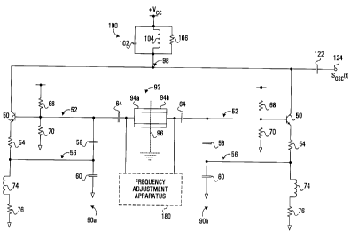
An oscillator design according to another preferred
embodiment of the present invention is depicted within FIGURE
6. This design comprises two balanced negative resistance
cells 90a,90b, similar to those described herein above for
the preferred embodiment depicted in FIGURE 4, these cells
operating with the resonator 92 as first and second
oscillators that are out-of-phase by approximately 180°. The
key difference between the embodiments of FIGURES 4 and 6 is
the outputting of the oscillation signals from the overall
oscillator. As can be seen in FIGURE 6, the resistors 53,
capacitors 72, coupling capacitors 78, and outputting
terminals 80 have been removed within the balanced negative
resistance cells 90a,90b. In place of these devices, the
collectors corresponding to the transistors 50 within FIGURE
6 have been coupled together at a node 98 and further coupled
to a tuned circuit 100 and an output terminal 124 via a
coupling capacitor 122.
The tuned circuit 100 preferably comprises a
capacitor 102, an inductor 104, and a resistor 106 coupled in
parallel between the power rail and the node 98. This tuned
circuit 100 is tuned to the second harmonic frequency of the
oscillators, that being twice the oscillation frequency
corresponding to the first and second oscillators in order to
11193ROCA02U ca o23osios Zooo-os-io
23
suppress the fundamental frequency and select out the second
harmonic. Although, in FIGURE 6, the tuned circuit 100
comprises a number of devices in parallel, this should not
limit the scope of the present invention. Alternatively,
other circuits that have a specific tuned frequency could be
utilized such as a single inductor or a quarter wave resonant
line.
Effectively, the single output at the output
terminal 124 of FIGURE 6 is a combination of the oscillation
signals from the first and second oscillators that are out-
of-phase by approximately 180°. FIGURES 7A and 7B illustrate
graphical depictions of possible voltage waveforms generated
by transistors 50 within the first and second negative
resistance cells 90a,90b respectively. Further, FIGURE 7C
depicts a possible voltage waveform combination of the
waveforms depicted in FIGURES 7A and 7B, this combined
waveform driving the tuned circuit 100 within FIGURE 6. As
can be seen in FIGURES 7A and 7B, the waveforms generated by
the transistors 50 are clipped sinusoidal signals that are
out-of-phase by 180°. The clipping in these signals can be
due to the transistors 50 going into compression as the
signal voltage is limited by a power rail or due to the
transistors 50 being shut off for a period of time as the
transistors are limited through cutoff. The result of a
combination of the voltage waveforms shown in FIGURES 7A and
7B, as depicted within FIGURE 7C, is a voltage waveform with
an overall oscillation frequency double that of each of the
first and second oscillators. This type of circuit, in which
two balanced oscillators generate two anti-phase clipped
signals at a first frequency and combine the clipped signals
to generate a signal at a second frequency twice the value of
11193ROCA02U ca o23osios Zooo-os-io
24
the first frequency, is known as a push-push oscillator. As
depicted within FIGURE 6, the use of the present invention
within a push-push oscillator design can allow for a
quadrupling of the resulting oscillation frequency when
compared to the frequency of resonance that would be achieved
using the resonator 92 within the oscillator of FIGURE 3.
A key advantage of the present invention is the
possibility of increasing an oscillation frequency beyond the
physical limitation commonly thought for a ceramic coaxial
resonator while still utilizing a ceramic coaxial resonator.
If utilized within a push-push oscillation design and the
system further has a subharmonically pumped mixer for
doubling the frequency, the present invention can increase
the range of use for a VC-CRO from approximately 20 GHz
(5x2x2) to approximately 40 GHz (5x2x2x2). This expansion in
frequency allows high frequency applications such as LMDS
applications to achieve the required frequency while still
using the advantageous ceramic coaxial resonators. All of
the advantages of the ceramic coaxial resonators as described
herein above are advantages of the present invention,
especially when considering applications requiring
frequencies higher than 20 GHz. In terms of the LMDS
applications, the DRO at a present cost of approximately
$500-600 can be replaced with a push-push oscillator as
depicted in FIGURE 6 at a cost less than $10, assuming a
subharmonically pumped mixer or doubler is implemented within
the system.
It should be understood that although the present
invention can be utilized by a system using a ceramic coaxial
resonator to raise the oscillation frequency to levels above
20 GHz, the present invention can also be utilized in
11193ROCA02U ca o23osios Zooo-os-io
implementations requiring lower frequencies. The present
invention does not have to be operated with the minimum size
ceramic coaxial resonator or with any other frequency
doubling techniques. There are possible advantages of the
5 present invention even at these lower frequencies when
compared to other oscillator designs. For instance, there
are advantages to using one large resonator within the push-
push oscillator design as depicted in FIGURE 6 rather than
using two resonators half the size within or using a single
10 resonator a quarter the size within a standard CRO as
depicted in FIGURE 3. For one, the resonator Q factor can be
increased by using a physically larger sized resonator that
can store an increased amount of energy. When using a single
large resonator in the push-push architecture of a preferred
15 embodiment of the present invention and then using the
technique discussed above to double the frequency to the
level of interest, the Q level for the resonator improves and
the phase noise can subsequently be reduced. Secondly, a
current disadvantage with balanced or push-push oscillator
20 design that use two resonators is that a shared isolated
ground plane is required to allow for a floating ground for
the resonators to be generated during operation. The need
for the isolated ground plane is a disadvantage the preferred
embodiments of the present invention depicted within FIGURES
25 4 and 6 do not have since the virtual ground is within the
resonator itself for these embodiments. Further, the lack of
an isolated ground plane allows the outside of the resonator
according to preferred embodiments of the present invention
to be grounded which increases its ability to be
manufactured.
Although the negative resistance cells 90a,90b have
I,
11193ROCA02U ca o23osios 2ooo-os-io
26
been described for the preferred embodiments herein above as
being balanced with the result being oscillation signals out-
of-phase by 180°, this is not meant to limit the scope of the
present invention. The present invention could be
implemented within embodiments in which the negative
resistance cells are balanced but not 180° out-of-phase, but
instead are out-of-phase by more or less degrees, generally
stated as being out-of-phase by a phase angle greater than
zero. For instance, an oscillator design, according to an
alternative embodiment of the present invention that does not
have resonators out-of-phase at 180°, comprises four
resonators coupled in a ring configuration with each end of a
resonator coupled to the end of another one of the
resonators. Further, the resonators are each in parallel
with an amplifier that can operate as a negative resistance
cell. In this case, four oscillation signals are generated,
one between each pair of resonators, with a 90° phase
difference between each. When these signals are combined, an
oscillating signal is generated at an oscillation frequency
four times the frequency of resonance for one of the utilized
resonators if implemented within the VC-CRO of FIGURE 3.
Further, despite the preferred embodiments being
directed to balanced oscillator embodiments, there are
possible
advantages to having embodiments of the present invention in
which the two negative resistance cells are not balanced.
Currently unbalanced oscillator designs utilizing the present
invention are being studied by the applicant of the present
invention. There currently appears to be possible advantages
of having one negative resistance cell tuned to a frequency
higher than the other negative resistance cell such that the
n
11193ROCA02U ca o23osios Zooo-os-io
27
virtual ground 96 is not at the center of the resonator 92.
The moving of the virtual ground 96 could possibly allow for
the effective dividing of a ceramic coaxial resonator into
smaller portions than halves, thus extending the potential
frequency of operation of a ceramic coaxial resonator.
Yet further, although the preferred embodiment of
the present invention is described with respect to negative
resistance cells of a Colpitts type, this is not meant to
limit the present invention. There are many well-known
apparatuses that function as negative resistance cells in
operation that can be coupled to either side of a coaxial
resonator to generate an oscillator that utilizes the present
invention. For example, FIGURE 8 illustrates the push-push
architecture of FIGURE 6 with the negative resistance cells
of the Colpitts type replaced with alternative negative
resistance cells 300a,300b. In this case, each of the
negative resistance cells 300a,300b comprise a transistor 302
with a collector coupled to the node 98 (and further coupled
to the other collector), a base coupled to a node 306 and an
emitter coupled to a node 308. The nodes 308 are each
further coupled to a respective end of the resonator 92 via
coupling capacitor 64. The nodes 306 are each further
coupled to an inductor 312 coupled between the node 306 and
ground, a first biasing resistor 314 coupled between the node
306 and the power rail, and a second biasing resistor 316
coupled between the node 306 and ground. The emitter biasing
in these negative resistance cells 300a,300b is achieved
through respective resistors 318 which are isolated from the
RF circuit by respective choke inductors 320 in series. The
remaining components depicted in FIGURE 8 have previously
been described herein above with reference to other
11193ROCA02U ca o23osios Zooo-os-io
28
embodiments. The overall operation of the push-push
oscillator depicted in FIGURE 8 is similar to the design of
FIGURE 6 but with a different configuration for the balanced
negative resistance cells. The end result is similar, that
being a quadrupling of the oscillation frequency at the
output terminal 124 compared to the traditional frequency of
resonance for the resonator 92 when in a setup as depicted in
FIGURE 3.
The preferred embodiments of the present invention
were described as VC-CROs. It should be recognized that with
the removal of the frequency adjustment apparatus 180, the
oscillators are simply CROs with no voltage control.
Although the oscillator circuits of the present
invention described herein above are operating at the
fundamental mode of the resonator, the circuits could
alternatively be designed to sustain oscillations at higher
order modes of the resonator.
Persons skilled in the art will appreciate that
there are yet more alternative implementations and
modifications possible for implementing the present
invention, and that the above implementation is only an
illustration of this embodiment of the invention. The scope
of the invention, therefore, is only to be limited by the
claims appended hereto.