Note: Descriptions are shown in the official language in which they were submitted.
CA 02308390 2000-04-13
WO 00/16503 PCT/CA99/00826
- 1 -
FREE SPACE OPTICAL INTERCONNECT SYSTEM
FIELD OF THE INVENTION
This application is a Continuation-in-Part of US
5 patent application aerial N0.09/150,242 to Dominic
Goodwill filed September 10, 1998 and incorporated herein
by reference. The present invention relates to a free
space optical interconnect system, in particular to a
system tolerant to misalignments.
io
BACKGROUND OF THE INVENTION
Free space optical interconnect systems have long
been proposed to deliver fast, highly parallel data
transfer. These systems have the potential to obviate
i5 limitations of electrical interconnects, which are not
capable of supporting data throughputs beyond a capacity
of several hundred Gb/s, and to increase the capacity up
to the Terabits range. Thus free space interconnect
systems are promising and attractive alternatives for
zo various telecommunication and computing applications.
However, the most important challenge preventing
the current acceptance of free space interconnect systems
is alignment. Two issues are of concern: the precision to
which it is possible to align the system, and the
25 precision to which it is necessary to maintain this
alignment during operation. For practical applications it
is necessary to establish and maintain alignment of
circuit boards carrying transmitters and receivers, which
may comprise an array of pixels, to within 10's of microns
30 over a distance of meters. Such a system requires
extremely expensive highly precision optomechanics, and to
date has been implemented only in a controlled laboratory
environment. In real product usage, when vibrations,
temperature fluctuations and temperature gradients are
3s encountered, the optical links move out of alignment and
data is not correctly transferred.
CA 02308390 2000-04-13
WO 00/16503 PCT/CA99/00826
- 2 -
Therefore, the goal of providing some alignment
tolerance for optical links is to ensure the correct
operation of all of the pixels on each array at the
highest possible speed. Correct operation is defined as
s the correct reception of a logic 1 or logic 0 signal. Once
the laser power, the receiver sensitivity and the detector
area have been defined, the probability of correct
reception of the logic bits is mainly a function of
optical beam misalignment. Misalignment mechanisms can be
io due solely to mechanical movements, but in practice,
optical effects can also contribute. Six degrees of
freedom of the mechanical movements: translation in x, y,
and z (0x, 0y, ~z) and rotation about the x, y, and z axes
(6x, 9Y, 9Z) , where x and y axes define the plane of an
i5 optical module in its nominal alignment position, with z
axis being perpendicular to this plane, result in a number
of optical effects. These include an image shift (fix, Dy),
image rotation ( 9Z) , defocus (0z) and image tilt (6x, Ay) .
Image shift and rotation are basically lateral translation
zo effects, and defocus and image tilt introduce defocus
effects. Contributors to the overall lateral misalignment
effects include:
mechanical misalignment in x and y;
mechanical rotation about the z axis;
zs mismatches in focal lengths;
wavelength shifts and laser mode-hops caused by
temperature fluctuations and resulting in beam deflections
introduced by diffractive elements;
distortions of the image of an array of sources
3o by the interconnect lens system, and
telecentricity, when defocus, in addition to
increasing spot size, introduces lateral misalignments in
nontelecentric systems.
Contributors to the overall defocus effects
as include:
source array tilt;
image tilt;
CA 02308390 2000-04-13
WO 00/16503 PCT/CA99/00826
- 3 -
curvature of the plane of best focus;
mechanical tilt about x and y axes;
misalignment along z axis.
Numerous attempts have been made to increase
5 alignment tolerance for optical interconnect systems which
may be categorized as passive, active, or dynamic
strategies.
However, passive alignment of dense, high speed
free space optical interconnects for distances of more
io than 1 cm require mechanical support structures that are
too expensive, difficult to align, and insufficiently
stable for commercial applications, see, e.g.,
"Optoelectronic ATM switch employing hybrid silicon
(MOS/GaAs) FET-SEEDS", A.L. Lentine et al., SPIE
15 Proceeding, vol. 2692, pages 110-108, 1996; and "Optical
bus implementation system using Selfoc lenses", K.
Namanaka, Optics Letters, Vol. 16, No. 16, pp. 1222-1224,
August, 1991. Passive alignment is done before any devices
are powered up. This alignment technique is used in almost
2o all electrical connectors, and most optical fiber
connectors are passive. Recently, solder bump techniques
have been applied to certain free space optical
interconnect components, and preliminary reports indicate
the potential for submicron alignment in all 6 degrees of
25 freedom over a scale of up to 1 cm, J.W. Parker "Optical
Interconnection for Advanced Processor Systems: A Review
of the ESPRIT II OLIVES Program", L. Lightwave Technology
9 (12), 1764-1773, 1991.
Active alignment requires some feedback about the
3o quality of the alignment. Usually the feedback is achieved
by illuminating the system and monitoring the alignment
either visually or by measuring a photocurrent in the
detectors. Real-time active alignment is necessary if the
alignment tolerances are tight or the system stability is
3s poor so that the system will not remain aligned for a
reasonable length of time. In this case, the feedback and
alignment actuators must be integrated into the system to
CA 02308390 2000-04-13
WO 00/16503 PCT/CA99/00826
- 4 -
ensure permanent alignment. For example, CANON
manufacturer uses image recognition and active beam-
steering using a liquid filled variable angle prism in a
single channel 155Mb/s link product, which currently costs
s $100K. The product uses built in viewing cameras and
optical pattern recognition techniques to define tY~e
system alignment, the complexity and cost of such a system
clearly limiting widespread application. Alternatively,
NTT has a system using actively controlled variable angle
io liquid filled prisms for board to board parallel free
space optical interconnect, see. e.g. "Optical beam
direction compensating system for board-to-board free
space optical interconnection in high-capacity ATM
switch", K. Hirabayashi et al., Journal of Lightwave
is Technology, Vol. 15, No. 5, May 1997. Cost, size,
environmental ruggedness and reliability of these systems
remain concerns.
Additionally, to develop both a marketable and
reliable system, devices have to be packaged in a useful
zo and reliable manner. For large systems including
cumbersome and bulky mechanical parts providing alignment,
this could involve an significant amount of physical space
just to house all the individual components.
Recently, a proposal for avoiding high precision
2s mechanics in free space interconnect systems by use of
redundant detectors has been put forward by F. A. P.
Tooley in IEEE Journal of Selected Topics in Quantum
Electronics April 1996, vol. 2, No. 1, pp. 3-13 and in
Digest, IEEE Summer Topical Meetings, August 5-9 1996, p.
30 55-56. This system increases tolerance to misalignment by
providing an array of detectors in place of a single
detector and electrically re-routing the misaligned
optical data to the correct channel, or, alternatively,
by replicating the signal a number of times. The overhead
3s associated with increasing the alignment tolerance
requires a control and router circuit, which adds
electrical power consumption.
CA 02308390 2000-04-13
WO 00/I6503 PCT/CA99/00826
Therefore a need exists for development of
alternative structures for free space optical interconnect
systems which would avoid high precision mechanics, while
providing precise alignment combined with simple design,
s reliability, low power consumption and compact packaging.
SUN~iARY OF THE INVENTION
Thus, the present invention seeks to provide an
optical interconnect system and method which avoid or
io reduce the above-mentioned problems.
Therefore, according to one aspect of the present
invention there is provided a free space optical
interconnect system comprising:
a transmitter and a receiver, at least one of the
i5 transmitter and the receiver comprising a plurality of
elements arranged into clusters, the number of clusters
being redundant and the number of elements in each cluster
being sufficient to accommodate the number of data
channels to be transmitted;
2o means for identifying a misalignment between the
transmitter and the receiver; and
means for re-routing data from the cluster which is
misaligned to a redundant cluster providing data
transmission through the system, the re-routing being
25 performed in response to a signal generated by the means
for identifying the misalignment.
Conveniently, the means for identifying the
misalignment comprises means for providing feedback
between the transmitter and the receiver regarding the
so misalignment.
In the first embodiment of the invention, the
number of elements in each cluster is equal to the number
of data channels to be transmitted. Alternatively the
number of elements in a cluster may be more than the
35 number of the transmitted data channels, with the means
for re-routing data between the clusters further
comprising means for re-routing data between the elements
CA 02308390 2000-04-13
WO 00/16503 PCT/CA99/00826
- 6 -
within a cluster. It is also possible to arrange that the
number of elements in each cluster is less than the number
of data channels to be transmitted, e.g. by using
transmitter elements capable of transmitting more than one
s data channel (multi-wavelength lasers). The number of
elements in different cluster may be equal or different-,
depending on the system requirements.
The elements of the transmitter and/or the receiver
may be arranged into clusters, the clusters preferably
to being arranged into a one-dimensional or two-dimensional
array, or any other pattern providing the required optical
transmission or collection. The elements within clusters
of the transmitter and/or receiver may also be arranged
into a pre-determined pattern, and individual elements may
i5 or may not be shared by different clusters. The system may
comprise one transmitter and one receiver only to provide
a uni-directional interconnection. Alternatively, the
system comprises two modules, each comprising one
transmitter and one receiver, thus providing for a bi-
2o directional data transmission and receiving of data.
Preferably, the system is implemented with
optical elements, such as bulk optics (lenses, prisms,
mirrors, splitters, et al.), binary optics (fanout
gratings, diffractive lenses, et al.), holographic
2s elements, and integrated optics.
Preferably, the elements of the transmitter are
optical emitters or optical modulators. The emitters may
be vertical cavity surface emitting lasers (VCSEL), light
emitting diodes (LED) and edge emitting laser diodes or
30 other known devices. The modulators may be modulators
based on magneto-optic effect, modulators including liquid
crystal devices, ferroelectric modulators, e.g. lead
lanthanum zirconate titanate (PLZT) modulator, modulators
including piezo-electric crystals, modulators including
35 deformable mirrors, electro-optical semiconductor hetero-
structure modulators, optical cavity modulators, or other
known modulators.
CA 02308390 2000-04-13
WO 00/16503 PCT/CA99/008Z6
The receiver of the optical interconnect system
comprises at least one detector, preferably from PIN
detector, metal-semiconductor-metal detector, avalanche
photodiode, ar other known detectors.
s To identify misalignments of the system, the system
includes identifying means, e.g. detectors for monitoring
lateral and vertical misalignments, detectors for
monitoring tilt misalignments, at least one dedicated
alignment laser and at least one dedicated detector, and
io means for monitoring a signal level at the dedicated
detector or detectors.
To provide feedback between the transmitter and the
receiver regarding misalignments of the system, the system
includes means providing a stable feedback mechanism which
is may be selected from optical fiber, LED, electrical cable,
electrical backplane, or other convenient means.
When misalignments of the system occur, each
cluster accommodates for misalignments within a
predetermined spatial and angular deviation, the data
2o being re-routed between clusters when the misalignment is
beyond the deviation. Preferably, means for re-routing of
data provide cycling through the clusters of at least one
of the transmitter and the receiver according to a
predetermined orthogonal pattern which ensures alignment
2s of the system. Alternatively, re-routing of data may be
done by cycling through the clusters at different rates or
any other method to provide alignment of the system. In
the case of a system redundancy both of lasers and of and
of detectors, preferably the lasers compensate for a gross
3o misalignment, and the detectors simultaneously make
additional fine compensation of misalignment. Preferably,
the transmitter and/or receiver, or, alternatively; the
whole system described are integrated within a package or
several packages, thus providing compactness and efficient
35 use of space.
According to another aspect of the invention
there is provided a method of compensating misalignments
CA 02308390 2000-04-13
WO 00/16503 PCT/CA99/00826
_ g _
in a free space optical interconnect system comprising a
transmitter and a receiver, at least one of the
transmitter and the receiver comprising a plurality of
elements whose number is redundant, the elements of at
s least one of the transmitter and the receiver being
arranged into clusters, the number of clusters being
redundant and the number of elements in each cluster being
sufficient to accommodate the number of data channels to
be transmitted, the method comprising the steps of:
io identifying a misalignment between the
transmitter and the receiver; and
re-routing data from the cluster which is
misaligned to a redundant cluster providing data
transmission through the system, the re-routing being
15 performed in response to a signal generated at the step of
identifying the misalignment.
Conveniently, the step of identifying the
misalignment further comprises sending a feedback signal
between the transmitter and the receiver regarding the
2o misalignment. Additionally, the method may further include
a step of arranging that the number of elements in each
cluster is equal to the number of data channels to be
transmitted. Alternatively, it may be arranged that the
number of elements in each cluster is not equal to the
2s number of the transmitted channels, e.g. being more than
the number of channels. In this situation, the step of re-
routing data between the clusters may further comprise re-
routing of data between the elements within a cluster.
Beneficially, the method provides a continuous
3o misalignment compensation of the system within a
predetermined angular and space deviation, the identifying
of misalignments being made by monitoring a signal level
at the receiver. Preferably, re-routing of data is
performed by cycling through the clusters according to a
35 predetermined orthogonal pattern or by cycling through the
clusters at different rates ensuring alignment of the
CA 02308390 2000-04-13
WO 00/16503 PCT/CA99/00826
_ g _
system, and the elements of the transmitter and/or
receiver may or may not be shared by different clusters.
According to yet another aspect of the invention
there is provided a method of compensating misalignments
s in a bi-directional free space optical interconnect system
comprising a first module and a second module, each module
having a transmitter and a receiver, at least one of the
transmitter and the receiver at each module comprising a
plurality of elements arranged into clusters, the number
io of clusters being redundant and the number of elements in
each cluster being sufficient to accommodate the number of
data channels to be transmitted, the method comprising the
steps of
(a) defining an orthogonal sequence of pairs of
i5 clusters, each pair comprising one cluster
from each module;
(b) choosing a first pair from the sequence;
(c) re-routing data to the selected pair of
clusters;
20 (d) monitoring corresponding signal levels of
the data at the receivers;
(e) comparing signal levels at the receivers
with predetermined threshold values;
(f) when the signal level at least at one of
2s the receivers is below the threshold value,
re-routing the data to the next pair of
clusters from the sequence and repeating
the steps (d) , (e) and (f) .
According to yet another aspect of the invention
so there is provided a module for a free space optical
interconnect system, comprising:
at least one of a transmitter and a receiver, at
least one of the transmitter and the receiver comprising a
plurality of elements arranged into clusters, the number
35 Of clusters being redundant and the number of elements in
each cluster being sufficient to accommodate the number of
data channels to be transmitted;
CA 02308390 2000-04-13
WO 00/16503 PCT/CA99/00826
- 10 -
means for re-routing data from the cluster which
is misaligned to a redundant cluster in response to
feedback identifying a misalignment of the module.
Conveniently, the number of elements in each
s cluster is equal to the number of data channels to be
transmitted. Alternatively, the number of elements in each
cluster may be more than the number of data channels to be
transmitted, with the means for re-routing data between
the clusters further comprising means for re-routing data
io between the elements within a cluster. It is also possible
to arrange that the number of the elements within the
cluster is less that the number of the data channels to be
transmitted, e.g. by using multi-wavelength lasers. The
number of elements in different clusters may be equal or
is different depending on the module requirements.
Conveniently, the module further comprises means
for identifying a misalignment of the module in the
system, which may include detectors for monitoring lateral
and vertical misalignments, detectors for monitoring tilt
2o misalignments, a dedicated alignment laser and a dedicated
detector, or means for monitoring a signal level at the
receiver.
Preferably, the clusters of the module are
arranged in a one-dimensional or two-dimensional array, or
2s any other pattern providing a required light transmission
or collection. The module may include one transmitter only
or one receiver only for corresponding uni-directional
transmittance or reception of data. Alternatively, the
module may include both a transmitter and a receiver for
3o corresponding transmitting and receiving of data in a bi-
directional optical interconnect system. The elements of
the transmitter and/or receiver may or may not be shared
by different clusters, the elements of the transmitter
being preferably optical emitters or optical modulators.
35 Preferably, the module described above is integrated
within a package.
CA 02308390 2000-04-13
WO 00/16503 PCT/CA99/00826
- 11 -
Free space interconnect systems formed using the
techniques described above are much more tolerant to
misalignments between circuit packs compared to electrical
connectors or other existing free space optical
5 interconnect systems. The use of redundant elements of the
transmitter, or redundant clusters of elements in the
transmitter or receiver modules obviates the need of
packaging which requires precise alignment and which is
often expensive and bulky. The interconnect systems based
Zo on the present invention have simpler mechanical design,
have no moving parts and may be implemented with lower
cost mechanics. As a result, they can be manufactured more
readily and at much lower cost, and providing higher
reliability at the same time.
15
BRIEF DESCRIPTION OF THE DRAV~TINGS
The invention will now be described in greater
detail with references to the attached drawings wherein:
Figure 1 illustrates a schematic view of the free
2o space optical interconnect system for a uni-directional
link according to a first embodiment of the invention;
Figure 2 illustrates an arrangement of the
transmitter elements into one-dimensional array of
clusters according to the embodiment of Figure 1;
25 Figure 3 illustrates misalignment compensation in
the embodiment of Figure 1.
Figure 4 illustrates a drive circuitry for the
transmitter according to the embodiment of Figure 1;
Figure 5 illustrates a schematic view of a free
3o space optical interconnect system according to a second
embodiment of the invention;
Figure 6 illustrates an arrangement of the
transmitter elements into two-dimensional array of
clusters according to the embodiment of Figure 5;
35 Figure 7 illustrates a schematic view of a free
space optical interconnect system for bi-directional link
according to a third embodiment of the invention;
CA 02308390 2000-04-13
WO 00/16503 PCT/CA99/00826
- 12 -
Figure 8 shows a flowchart for a method for
misalignment compensation based on hunting algorithm;
Figure 9 illustrates misalignment compensation in
the embodiment of Figure 7:
s Figure 10 illustrates a schematic view of a two-
dimensional arrangement of lasers in a free space optical
interconnect system according to a fourth embodiment of
the invention;
Figure 11 illustrates a two-dimensional
io arrangement of detectors corresponding to the arrangement
of lasers of Fig. 10; and
Figure 12 illustrates a sub-circuitry for the
receiver according to the fourth embodiment of the
invention.
is
DETAILED DESCRIPTION OF THE PREFERRED E1~ODIMENTS
A schematic view of a free space optical
interconnect system 10 according to a first embodiment of
the present invention is shown in Figure 1. The system 10
2o comprises a first module 12, the module being a
transmitter module, and a second module 14, the module
being a receiver module, and provides a uni-directional
link between the modules. The transmitter module 12
carries a transmitter 16 having a plurality of transmitter
zs elements 18 (shown in Fig. 2) for transmission of data,
the receiver module carrying the corresponding receiver 20
having a plurality of receiver elements 22 for receiving
the data. Each of the transmitter elements 18 is a
vertical cavity surface emitting laser (VCSEL), emitting a
3o beam normal to the plane of the module 12 through the lens
32 of the transmitter package 16, and the receiver
elements 22 are detectors, preferably forming a one-
dimensional array. The lasers 18 are arranged into
clusters 26, 28 and 30, and as a way of example, the
3s number of lasers in each cluster being equal to the number
of data channels to be transmitted. The number of clusters
is redundant, i.e. the system includes more lasers than
CA 02308390 2000-04-13
WO 00/16503 PCT/CA99/00826
- 13 -
are necessary to transmit the data, the lasers being
assigned to clusters either permanently when they are not
shared by different clusters or dynamically when lasers
are shared by different clusters if needed (see below).
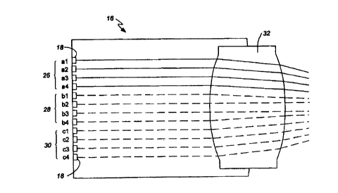
s An arrangement of the transmitter elements 18 is
shown in more detail in Figure 2. The transmitter 16 i-s
designed to support/transfer 4 data channels. It includes
twelve lasers 18 which form three clusters 26, 28, and 30
having elements (al, a2, a3, a4), (bl, b2, b3, b4) and
io (cl, c2, c3, c4), correspondingly as shown in Fig. 2, the
distance between the adjacent lasers being 0.25 mm to 1.25
mm. Thus, the number of elements in each cluster is equal
to the number of data channels to be transmitted, and the
system supports four data channels with 3-fold redundancy.
i5 The clusters 26, 28 and 30 and the lasers 18 within the
clusters form a one-dimensional array as shown in Fig. 2.
The lasers 18 are housed together with driver circuits 50
in a package on the transmitter module 12. Laser beams
from lasers 18 are emitted through the lens 32 collimating
20 or nearly collimating the light and received at the
detector array 22 being focused on the array through the
lens 34. The detectors 22 are housed together with
receiver circuits 23 in a package on the receiver module
14 .
2s Means for identifying a misalignment between the
transmitter 16 and the receiver 20 is implemented by use
of a dedicated alignment laser 36 packaged with a lens 38
(Fig.l) so as to emit a narrow beam perpendicular to the
transmitter module 12. The beam is received by a large
3o slow position sensing alignment detector 40 carried by the
receiver module 14 which monitors the mutual alignment of
modules 12 and 14, and as a result, the alignment of the
transmitter 16 and the receiver 20. Means for providing
feedback regarding the misalignment between the modules is
3s implemented by use of control circuitry 42 and 44 at the
transmitter and receiver modules correspondingly, light
emitting diode (LED) 46 at the receiver module 14, and a
CA 02308390 2000-04-13
WO 00/16503 PCT/CA99/00826
- 14 -
feedback detector 48 at the transmitter module 12. The
transmitter 16 also includes means for re-routing data
between clusters implemented by use of drive circuitry 50.
shown in detail in Figure 3 and described below.
s The system 10 operates in the following manner.
First, the data to be transmitted are routed to one of the
clusters 26. 28. 30, for example, the cluster 28 as shown
in Fig. I, the lasers 18 of the cluster emitting light
which is collimated by lens 32 and sent to the receiver
io 20. The focusing lens 34 collects the light from the
lasers 18, and produces one spot from each activated laser
on the detectors 22. Simultaneously, the alignment laser
36 sends a reference beam through the lens 38, and the
beam is received by a position sensing alignment detector
i5 40. The position of the reference beam on the detector 40,
and consequently the position of the module 14, is read
out by a control circuit 44, and the position information
is fed back by the LED 46 to a feedback detector 48 and
the laser control circuit 42 on the first module 12. If
2o the modules 12 and 14 are misaligned as shown in Fig. 3,
the laser beams generated by the cluster 28 do not hit the
detectors 22, and the data is lost. The drive circuit 50
re-routes the data to be transmitted to another cluster,
e.g. the cluster 26 in Fig. 3, which sends the data to the
2s correct physical location at the detectors 22, thus
compensating for the measured misalignment.
The drive circuit 50 shown in detail in Figure 4
operates in the following manner. Data to be transmitted
is presented to the drive circuitry on 4 data channel
3o inputs 52, 54, 56, 58 as digital logic signals, which are
converted by laser drive amplifiers 53. 55~ 57, 59
respectively into the signal levels required to drive the
lasers in the clusters 26, 28 30. The control circuit 44
generates digital signals on control inputs 60. 70, 80,
ss which cause pass transistors 62 to be open or closed, so
as to connect the data channel input 52 to laser a1, bl ,
or cl, input 54 - to laser a2, b2, or c2, input 56 - to
CA 02308390 2000-04-13
WO 00/16503 PCT/CA99/00826
- 15 -
laser a3, b3, or c3, and input 58 - to laser a4, b4 or
c4.
The system 10 is packaged in the following
manner. The transmitter module 12 and receiver module 14
s comprise part of printed circuit boards. The printed
circuit boards are mounted in shelves, racks and frame
made of plastic and metal. The printed circuit boards,
shelves, racks and frames have holes and windows as
necessary to allow the data, alignment and feedback light
io to pass. The laser clusters 26, 28. 30, the drive circuit
50 and the lens 32 are mounted using adhesives within a
metal and ceramic multi-chip package, and the package is
soldered onto the substrate of the transmitter module 12.
Likewise, the detectors 22, the receiver circuit 23 and
is the lens 34 are similarly packaged and mounted.
Power consumption in the transmitter 16 is
minimized by the sharing of laser drive amplifiers 53, 55,
57, 59 by three lasers each. The power consumed by each
laser drive amplifier 53, 55, 57, 59 is about 0.25 W, and
2a the whole 4-channel transmitter 16 consumes a power of
about 1 W. The heat generated is dissipated by the metal
and ceramic package of the transmitter 16. The system is
capable of providing efficient heat dissipation for number
of channels up to fifty and/or redundancy of nine-fold or
zs more.
The optical interconnect system 10 described
above has the following dimensions: separation between
modules 12 and 14 is about ~10 inches, focal lengths of
the lenses 32 and 34 are about 10 mm, an angle between the
30 laser beams generated by adjacent clusters, designated by
numeral 19 in Fig. l, is about 1 degree. These dimensions
provided about 4 mm alignment tolerance over 10 inches of
interconnect distance. Other dimensions of the system may
be also used to provide alignment of the system for larger
3s distances, e.g. up to meters.
Instead of the system above providing one-
directional link, an alternative embodiment of the system
CA 02308390 2000-04-13
WO 00/16503 PCT/CA99/008Z6
- 16 -
provides a bi-directional link, having one transmitter and
one receiver at each module for corresponding
transmittance and reception of data.
In the embodiment described above, the number of
s the elements in each cluster is equal to the number of the
data channels to be transmitted. It is also contemplated
that other embodiments of the invention may comprise
clusters of elements whose number is not equal to the
number of the transmitted data channels. For example, the
io number of elements in a cluster may exceed the number of
channels. Then it would be convenient to arrange for the
re-routing means to includes additional means providing
re-routing of data between the elements within each
cluster. It is also possible to have the number of
i5 elements in each cluster less than the number of data
channels, e.g. by using multi-wavelength lasers, each
capable of transmitting multiple data channels. The number
of elements in different cluster may be equal or
different, depending on the system requirements.
2o In another embodiment it is contemplated that the
elements of the receiver 20 only may be arranged into
clusters in a way similar .to that described above.
Alternatively, the elements of both of the transmitter 16
and the receiver 20 may be arranged into redundant
2s clusters. Correspondingly, re-routing of data would be
performed then between redundant clusters of the receiver
20 or the transmitter 16, or both of them depending on the
amplitude and type of misalignments of the system. In
this embodiment, the transmitter 16 compensates for gross
3o misalignments, and the receiver 20 makes additional fine
compensation of misalignment.
Numerous modifications can be made to the
embodiments described above. The elements 18 of the
transmitter 16 chosen to be VCSEL in the first embodiment
3s may be substituted by other types of emitters or optical
modulators. The emitters may be VCSEL, LED, edge emitting
laser diodes, or other known devices. The modulators may
CA 02308390 2000-04-13
WO 00/16503 PCT/CA99/00826
- 17 -
be selected from modulators based on magneto-optic effect,
modulators including liquid crystal devices, ferroelectric
modulators, e.g. PLZT modulators, modulators including
piezo-electric crystals, modulators including deformable
s mirrors, electro-optical semiconductor hetero-structure
modulators, optical cavity modulators, or other known
modulators. Similarly, other modifications of the
embodiment may include use of integrated optics components
(holographic elements, fanout gratings, diffractive
io lenses? and/or other bulk optical elements, e.g. arrays of
microlenses, prisms and splitters instead of lenses used
for collimating and focusing laser beams, or other known
optical components. The receiver elements may be a
detector array or a single detector, the light may fall
is directly onto detectors, or a microlens concentrator array
can be included which enhances the misalignment tolerance
and increase the efficiency of Light collection.
Modifications to the means for identifying misalignments
between the modules may include detectors for monitoring
20 lateral and vertical misalignments, detectors for
monitoring tilt misalignments, or means for monitoring a
signal level at the receiver, e.g. a detector measuring a
photocurrent at the receiver, or other suitable devices.
The transmitter elements may have a separate lens from the
2s lens of the alignment laser, or the transmitter elements
and the alignment laser may share a lens. The detectors
may be chosen from PIN detectors, metal-semiconductor-
metal detector, avalanche photodiode, or other suitable
detectors.
30 Further modifications to the system may include
different means for providing feedback between the
transmitter and the receiver regarding the misalignments,
which may be connected by optical fiber, electrical cable,
electrical backplane, or other convenient means.
3s Re-routing of data between clusters may be done
in different ways, e.g. the data may be re-routed between
clusters by cycling through the clusters of at least one
CA 02308390 2000-04-13
WO 00/16503 PCT/CA99/00826
- 18 -
of the transmitter and the receiver according to a
predetermined orthogonal pattern, i.e. according to a
particular sequence of clusters which ensures an alignment
of the system. Alternatively, for a system providing a bi-
5 directional link, cycling through the clusters may be
performed according to the orthogonal sequence of pairs of
clusters, or by cycling through the different sets of
clusters at different rates, e.g. clusters of the
transmitter are cycled at a different rate than clusters
io of the transmitter, ensuring overall that the system is
aligned. In addition, cycling through the clusters may
proceed in an order which is calculated to take the least
time on average, e.g. by starting with clusters which are
closest to the most recently used clusters so as to
is compensate rapidly for small misalignments, or by starting
with clusters close to the center of the laser and/or
detector arrays. Cycling through the clusters may be done
by first selecting simultaneously all the clusters in one
half of the transmitter and/or receiver array, then
2o selecting successively 50% fewer clusters in one or more
interactive steps based on the success or failure of the
clusters selected in the previous step, until the good
cluster is uniquely determined.
To reduce component count and physical size, the
25 elements of the transmitter and/or receiver may be shared
by two or more clusters. For example, in the embodiment
described above the number of lasers may be less than 12
in total and same lasers may be assigned to different
clusters. In this case each laser will carry a different
3o data channel depending on which cluster is activated.
Similarly, the receiver elements can be shared by one or
more clusters if the receiver elements are arranged into
clusters. The number and/or arrangement of clusters to
which a layer or a receiver element is assigned may be
3s changed in real time to meet a varying demand of traffic
patterns through the system. In the embodiment described
above, the interconnection is formed between two modules,
CA 02308390 2000-04-13
WO 00/16503 PCT/CA99/008Z6
- 19 -
each of the modules may be a board, a chip, an equipment
rack, an equipment shelf or an equipment frame. The
transmitters and receivers may be housed in different
packages, they may be built as separate chips within the
s same package, or they may be placed on the same chip.
A free space optical interconnect system 10~
according to a second embodiment of the invention is shown
schematically in Fig. 5. The system provides a uni-
directional link and comprises a transmitter module 112
io and a receiver module 114 carrying a transmitter 116 and a
receiver 120 correspondingly, the transmitter 116 having a
plurality of lasers (transmitter elements) 118 arranged
into a two-dimensional array of clusters 123-131 shown in
detail in Fig. 6, and the receiver 120 having a plurality
i5 of detectors 122. The system 100 also includes control
units 142 and 144 at the transmitter and receiver modules
112 and 114 correspondingly, means for identifying
misalignments implemented by use of circuitry 160
measuring photocurrent from the detectors (receiver
2o elements) 122, and means for providing feedback between
the transmitter and the receiver regarding the
misalignment of the system implemented by use of control
units 142 and 144 through an electrical cable connection
146. The system also includes drive circuitry 150 (not
2s shown in detail) similar to that of Fig. 3, but providing
a two-dimensional re-routing between clusters, and
receiver circuitry 167.
By way of example, the system shown in Fig. 5 and
6 supports 4 data channels with 3-fold redundancy in two
so dimensions (horizontal x and vertical y) which requires 36
lasers in total arranged into nine clusters designated by
numerals 123 to 131. Each cluster has 4 lasers arranged in
a square, e.g. clusters 123 and 131 have elements (aal,
aa2, aa3, aa4) and (ccl, cc2, cc3, cc4) respectively. The
35 distance between the adjacent lasers is about 0.25 mm, and
the nine clusters form a 3 x 3 array, with the center of
the clusters being on a 1.25mm pitch. The laser clusters
CA 02308390 2000-04-13
WO 00/16503 PCT/CA99/00826
- 20 -
123-131 are offset from each other across the surface of
the transmitter module 112. Thus, after passing through
the collimation lens 132, each laser cluster produces
beams directed at different angles in a three dimensional
s space.
The system 100 operates in the following manner-.
Data to be transmitted, being initially routed to one of
the clusters 123-131 of the transmitter 116, are sent
through the lens 132 collimating the light and received at
io the detectors 122 of the receiver 120 being focused by
lens 134. The circuitry 160 measures a photocurrent at the
detectors 122 and compares it with predetermined threshold
values for each detector. The results of the measurements
are processed by a control circuit 144, and a feedback
is signal regarding a misalignment is sent back to the
control circuit 142 of the transmitter module 112 via
electrical cable 146. In response to the feedback signal,
the control circuit 142 selects which cluster to use to
correct for physical misalignment, and the drive circuitry
20 150 re-routes the data to another cluster which emits
beams in the approximately correct direction and location.
It is also contemplated that other embodiments of
the invention may comprise other two-dimensional
arrangements of the clusters to form patterns such as a
2s square grid, a circle, ellipse, octagon, cross, or star,
or more complex patterns to achieve the required light
transmission or collection. Additionally, each cluster
itself may comprise elements arranged into a pre-
determined pattern, the elements of the transmitter and/or
3o receiver being arranged into clusters. In general, the
spatial pattern defined by the receiver clusters does not
need to match that formed by the transmitter clusters.
Additionally, the clusters may be spatially discrete as in
the embodiment of Fig. 5, or the clusters may be
as interleaved. The transmitter or receiver elements may be
shared by different clusters and other modifications
CA 02308390 2000-04-13
WO 00/16503 PCT/CA99/00826
- 21 -
similar to ones of the first embodiment listed above are
also applicable to the second embodiment of the invention.
A free space optical interconnect system 200
according to a third embodiment of the invention is
s schematically shown in Fig. 7. The system comprises a
first module 212 and a second module 214, the first module
carrying a first transmitter 215 and a first receiver 216,
the second module carrying a second receiver 217 and a
second transmitter 219. Each of the transmitters 215 and
10 219 has a plurality of transmitter elements 218 (not
shown) for transmittance of data, each of the receivers
216 and 217 having a plurality of receiver elements 220
for receiving the data. The transmitter elements 218 are
vertical cavity surface emitting lasers (VCSEL), emitting
is beams normal to the planes of the modules 212 and 214. The
elements 222 of the receivers 216 and 217 are detectors
forming one-dimensional arrays 227 and 228 respectively,
the detector arrays 216 and 217 being connected to the
receiver circuit arrays 267 and 269 respectively. The
20 lasers 218 of the first transmitter 215 are arranged into
clusters 221,222,223, the lasers of the second transmitter
219 being arranged into clusters 224, 225, 226. Similar to
the embodiments described above, the number of clusters at
each of the transmitters is redundant, and the number of
2s lasers in each cluster is equal to the number of data
channels to be transmitted. An arrangement of the
transmitter elements 218 into clusters at the modules 215
and 219 is similar to that one shown in Figure 2. Laser
beams from the clusters at the modules 215 and 219 are
3o emitted through respective lenses 232 and 233 which
collimate or nearly collimate the light, and are detected
at detector arrays 228 and 227 correspondingly, being
focused on the arrays through lenses 234 and 235. The
system further includes the following components at each
3s of the first and second modules correspondingly: control
circuitry 242 and 244, thresholding circuitry 260 and 261
for measuring signal levels at the receivers 216 and 217,
CA 02308390 2000-04-13
WO 00/16503 PCT/CA99/00826
- 22 -
drive circuitry 250 and 251 for re-routing data between
clusters of the transmitters 215 and 219 similar to that
shown in Fig. 4.
Advantageously, in this embodiment a separate
s feedback connection, (e. g. electrical cable, electrical
backplane, optical fiber or LED) is not required. The
transmitters 215, 219 and the receivers 216. 217 serve the
purpose at different times of transferring traffic data
and of exchanging alignment information. The process of
io establishing alignment between clusters in the system 200
is illustrated by a flowchart shown in Fig. 8. Upon start
up (block 302), the routine 300 representing the hunting
algorithm for re-routing clusters defines module 212 as
"master" and module 214 as "slave", and performs an
is alignment setup (block 302) which determines a unique
orthogonal sequence of clusters for cycling to ensure that
the system steps through all possible alignment
compensations. For the system 200, the orthogonal sequence
is a sequence of pairs of clusters where each pair
2o comprises one cluster from each module. The system
ensures that the system steps through all the possible
alignment compensations within a pre-determined range. The
sequence is pre-determined and stored in local memories
(not shown). The modules 212, 214 select (blocks 306, 326)
zs the next cluster on each module from the orthogonal
sequence, and a known preamble character is sent (blocks
308, 328) from the selected clusters of the transmitters
215, 219 respectively by appropriately routing the
preamble character through the drive circuits 250, 251
ao respectively. Light from the transmitters 215, 219 is
received by detector arrays 228, 227 respectively (blocks
310 330). Thresholding circuits 261 and 260 in modules
214 and 212 respectively filter and compare (blocks 312,
332) the signals from the detector arrays 228, 227
3s respectively to determine (blocks 314, 334) whether the
signals exceed a pre-determined threshold value, sending
the results of the determination to control circuits 244
CA 02308390 2000-04-13
WO 00/16503 PCT/CA99/00826
- 23 -
and 242 respectively as electrical signals (not shown).
Control circuit 242 then sets a "Slave laser" flag to TRUE
(block 336) or FALSE (block 338) depending on the result
of block 334, where TRUE indicates that the preamble
s character has been correctly received by receiver 216.
Simultaneously, depending on the result of block 314
control circuit 244 causes transmitter 219 to transmit
either a predetermined "YES" character (block 316) or no
signal (block 318), where a "YES" character indicates that
io the preamble character has been correctly received by
receiver 217. If a "YES" character is then received (block
320), using receiver 216 and thresholding circuit 260,
then control circuit 242 sets (block 322) a "Master laser"
flag to TRUE, otherwise the control circuitry 242 sets
is (block 324) a "Master laser" flag to FALSE. Control
circuitry 242 then determines (block 340) whether both the
"Slave laser" flag and the "Master laser flag" are TRUE.
If either flag is FALSE the alignment is not yet
accomplished and the routine 300 loops from blocks 306 and
ao 326. If both flags are TRUE, then the alignment is
complete and the most recently selected clusters
correspond to correct alignment, and the system sends
traffic using those selected clusters (block 342).
The alignment setup routine 300 can be performed
2s just once when the system is first turned on, when a new
board is inserted, or it can be performed repeatedly to
compensate for real-time drift or vibration.
Fig. 9 illustrates a process of the alignment of
the system 200. For example, when the module 214 is tilted
3o as shown in Fig. 9, the algorithm described above
determines a correct pair of clusters, namely cluster 221
at the transmitter 215 and cluster 224 at the transmitter
219, which provide transmittance of the data to the
correct physical locations at the corresponding receivers
35 2I7 and 216. The dimensions of the system 200 are similar
to that of the first embodiment, namely a separation
between modules 212 and 214 is about 10 inches, focal
CA 02308390 2000-04-13
WO 00/16503 PCT/CA99/00826
- 24 -
lengths of the lenses 232 and 233 are about 10 mm, an
angle between the laser beams generated by the adjacent
clusters is about 1 degree, thus allowing for about 4 mm
alignment tolerance over 10 inches of interconnect
s distance.
It is also contemplated that in other
embodiments, the elements of the receiver or both of the
transmitter and the receiver, are arranged into clusters,
the clusters forming one or two dimensional patterns of
io different configurations. The numbers of data channels
transmitted in both directions from one module to the
other one may be different, the hunting algorithm
described above may be modified for cycling through
clusters of different modules at different rates, the
is elements of the transmitters and/or receiver may be shared
by different clusters, the system may provide a uni-
directional or bi-directional link, the receiver elements
may be single detectors or detector arrays. Other
modifications described above in relation to other
2o embodiments are also applicable to the third embodiment of
the invention.
A free space optical interconnect system
according to a fourth embodiment of the invention is
similar to that of Figure 5 except for the elements of
2s both the transmitter and receiver being arranged into
clusters and the number of elements in a cluster being
more than the number of data channels. Aspects of this
embodiment are shown in Fig. 10, Fig. 11 and Fig. 12. As a
way of example, a laser array 402 of the transmitter
3o transmits five data channels using six transmitter
elements. Correspondingly, the receiver containing a
detector array 422 receives five data channels using six
receiver elements. Spare elements are used in the event of
failure of the laser in one of the other five elements, or
3s in the event of failure of one of the five connections due
to a misalignment or a piece of dust. The laser array 402
comprises lasers that are arranged spatially at the
CA 02308390 2000-04-13
WO 00116503 PCT/CA99/00826
- 25 -
vertices of a tessellated array of hexagons, with a laser
cluster 404 consisting of the six lasers of a hexagon,
with five lasers 406, 408, 410, 412, 414 of the laser
cluster being used initially and the sixth laser 416 of
s the laser cluster being a spare. The detector array 422
comprises detectors that are arranged spatially at the
vertices of a tessellated array of rhombuses with the
length of the edge of each rhombus being equal to the
length of the edge of the hexagon of the laser cluster
io 404, with a detector cluster 424 consisting of the six
detectors in a hexagon, with five of the detectors 426,
428, 430, 432, 434 of the detector cluster being used
initially, and the sixth detector 436 of the detector
cluster being a spare. Initially, the lasers 406, 408,
is 410, 412, 414 and detectors 426, 428, 430, 432, 434 are
used to carry the five data channels respectively. In the
event of a failure of one of these lasers or detectors or
another element or elements of the data path, the data of
the failed channel is routed through the spare laser 416
2o and the spare detector 436.
Each set of clusters has an associated receiver
sub-circuit shown in Fig. 12. The detectors 446, 448, 450,
452, 454, 456 of a cluster have amplifier circuits 466,
468, 470, 472, 474, 476 respectively, the amplifier
2s circuit of the first five detectors producing signal
outputs that are connected to gates 486, 488, 490, 492,
494 respectively and the amplifier circuit 476 of the
sixth detector producing a signal output that is connected
in parallel to gates 506, 508, 510, 512, 514. A detector
ao signal level for each detector is also identified by the
amplifier circuits and is passed to a controller 464 using
a set of electrical connections 462.
The receiver sub-circuit operates in the
following manner. Initially, the controller opens the
3s gates 486, 488, 490, 492, 494 and shuts the gates 506,
508, 510, 512, 514, so as to route the data signals from
the first five detectors to the five data channel outputs
CA 02308390 2000-04-13
WO 00/16503 PCT/CA99/00826
- 26 -
526, 528, 530, 532, 534 respectively. If the detector
signal level for one of the first five detectors is
determined by the controller 464 to indicate that a
detector is not receiving the correct signal level and
s that therefore the channel has failed, then the data from
the spare detector 436 is routed to the corresponding data
channel output by shutting the appropriate gate from the
set 486, 488, 490, 492, 494 and opening the appropriate
gate from the set 506, 508, 510, 512, 514, at the same
io time as a transmitter circuit (not shown) routes the
transmitted signal of the failed channel to the spare
transmitter laser 416.
It is also contemplated that the controller may
examine the detector signal levels only once when a
i5 cluster is first selected, or each time a cluster is
selected, or continuously during operation of the system.
The number of spare channels may be zero, one, or more
than one. Clusters at different locations across the laser
and detector arrays may have a different number of spare
2o channels. Other modifications described above in relation
to other embodiments are also applicable to the fourth
embodiment of the invention.
Free space interconnect systems formed using the
techniques described above are more tolerant to
2s misalignments between circuit packs compared to electrical
connectors or other existing free space optical
interconnect systems. The use of redundant clusters of
elements in the transmitter and/or receiver modules
obviates the need of packaging which requires precise
3o alignment and which is often expensive and bulky. The
interconnect systems based on the present invention have
simpler mechanical design, have no moving parts and may be
implemented with lower cost mechanics. As a result, they
can be manufactured more readily and at much lower cost,
35 providing higher reliability at the same time. For
example, using the embodiments of the invention, a free
space optical link offering multiple channels (>32 per sq.
CA 02308390 2000-04-13
WO 00/16503 PCT/CA99/00826
- 27 -
in.) at a rate of about 1Gb/s each can be established in
the conventional low cost mechanical environment typically
encountered with telecom, data and computing products. The
optical interconnect system described above is
s particularly advantageous for high capacity ATM and IP
switches for core or larger enterprise customers and operra
new possibilities for new systems architectures and
network technologies for terabit routers, and for multi-
processor computers.
io Although specific embodiments of the invention
have been described in detail, it will be apparent to one
skilled in the art that variations and modifications to
the embodiments may be made within the scope of the
following claims.