Note: Descriptions are shown in the official language in which they were submitted.
CA 02308473 2000-OS-02
WO 99n6426 PCT/US98/24447
1
SYSTEM AND METHOD FOR ELECTRONICALLY IDENTIFYING
CONNECTIONS OF A CROSS-CONNECT SYSTEM
BACKGROUND OF THE INVENTION
The present invention relates generally to communications systems, and
more particularly, to a system and method for electronically identifying all
connections established through a cross-connect system. .
Cross-connect systems are widely used in the telecommunications
industry to effect signal line connections between various types of
communications equipment managed by different information service providers.
Within a central office or exchange environment, for example, tens of
thousands
of information signal lines from a first communications equipment facility
must
be connected to respective signal lines from a second communications
2 o equipment facility in a manner that provides for a high degree of
connection
reliability. To this end, industry-standard cross-connect systems typically
utilize
highly-reliable passive connection devices, often termed cross-connect
circuits,
to effect the required signal line connections. In a typical application, a
pair of
cross-connect circuits are used to connect a single signal line of a first
equipment
facility with a single signal line of a second equipment facility.
Identifying the specific location and determining the status of all cross-
connected circuits within a central office has heretofore required varying
degrees
of manual intervention, such as manually tracing a hard-wired or temporary
patch connection in an effort to identify the location of the cross-connect
circuits
3 0 terminating opposing ends of each connection. It can be readily
appreciated that
manually acquiring connection information and updating this information on a
regular basis represents a sizable and costly challenge.
CA 02308473 2000-OS-02
WO 99/26426 PCTNS98/~4447
2
It would appear that introducing active electronic components within the
information signal paths would provide the opportunity to implement a cost
effective and efficient means of acquiring connection information for a cross-
connect system. A number of proposed prior art solutions require the
introduction of active electronics into the information signal paths in order
to
effect transmissions between cross-connected circuits. Various time-sharing
and
frequency multiplexing schemes have been proposed that require sharing of the
information signal paths, in terms of transmission time or fiequency
bandwidth,
which necessarily require the implementation of a collision detection and
resolution scheme in order to reduce the likelihood of disturbing information
signal transmissions over the connections.
Introducing active components into the information signal circuit paths,
however, has proven to systemically reduce the overall reliability of certain
cross-connect systems to unacceptable levels. The possibility of information
signal disruption and the possible malfunction or failure of the active
electronics
within the information signal conductivity path has prompted most, if not all,
manufacturers of cross-connect systems to exclusively use passive cross-
connect
components within the information signal path. Although passive connection
devices provide a requisite level of reliability, such passive devices
significantly
2 0 complicate the effort of developing a fully automatic, electronic
implementation
for identifying the location and status of all cross-connected circuits and
connections established through a central office. The present invention
provides
such an implementation.
CA 02308473 2000-OS-02
wo ~nt~z6 rcrnJS~
3
SUMMARY OF THE INVENTION
The present invention is directed to a system and method for
electronically identifying connections established through a cmss-connect
system. The present invention provides for the identification of all hard-
wired
and temporary patch connections, and any modifications made to existing cross-
connect circuit connections. Connection identification and status information
is
acquired in near real-time and stored in a database which is accessible by a
user
through a graphical user interface (GUI).
TRACE or lamp wires, which are connected between respective pairs of
cross-connect circuits in accordance with a standard industry practice, are
utilized in an unconventional manner so as to form a scanning bus. The
information signal paths established through the cross-connect circuits remain
undisturbed. A scanning signal is communicated between each pair of cross-
connected circuits over the TRACE conductor. In the event a patch cord is used
to temporarily redirect a signal connection, the scanning signal is
transmitted
over the shield or sleeve conductor of the patch cord, the patch cord shield
thus
being incorporated as part of the overall scanning bus. The scanning signal
provides identification and other information concerning the transmitting
circuit.
2 o A circuit receiving the scanning signal communicates its identification
information and that of the transmitting circuit derived from the scanning
signal
to a central computer. The identification information acquired by the central
computer from all receiving cross-connect circuits provides identification and
status infornnation for all circuits within the cross-connect system. In one
2 5 embodiment, alI circuits of a cross-connect system are scanned and
identification
information acquired in the time required to transmit a single cross-connect
circuit ID bit string, irrespective of the total number of cross-connect
circuits
included within the cross-connect system.
CA 02308473 2000-OS-02
WO 99/~64Z6 PCTIUSg8124447
4
Various types of information concerning each connection established
within a cross-connect system is maintains in a database and updated in near
real-time so as to reflect the current state of alI circuit connections. A
graphical
user interface cooperates with the database to provide a user the ability to
access
connection records of interest, to visually display simulated depictions of
selected connections, and to generate a variety of reports derived from the
connection information maintained in the database. The graphical user
interface
may also be used to guide a technician to specific circuit locations to effect
repairs, establish a new connection or redirect an existing connection thmugh
use
of a patch cord.
A "patch pending" file may be created which indicates various
connections or disconnections to be effected by a technician to accomplish a
particular objective. A patch pending file typically contains information
identifying the specific sequence by which patch cord installation or removal
is
to be accomplished. When executed, the patch pending file may control multi-
colored TRACE LEDs of specified circuits as a means of visually directing the
work of a technician when establishing and breaking cross-connections.
A patch pending file may also be created to provide information
concerning contingent or back-up connections that may be established in the
2 o event of a network outage. Such a patch pending file may identify
important
circuits which require immediate restoration during temporary or extended
outages. Upon occurrence of an actual system outage, an appropriate patch
pending file may be selected and executed to implement an efficient,
coordinated
patching procedure for restoring key circuits.
2 5 The above summary of the present invention is not intended to describe
each embodiment or every implementation of the present invention. Advantages
and attainments, together with a more complete understanding of the invention,
will become apparent and appreciated by referring to the following detailed
description and claims taken in conjunction with the accompanying drawings.
CA 02308473 2000-OS-02
WO 99/26426 PCT/US98I24417
BRIEF DESCRIPTION OF THE DRAWINGS
5 Fig. 1 is an illustration of a cross-connect apparatus which is typically
employed by an information service provider for terminating, cross-connecting,
and accessing a number of communication lines;
Fig. 2 is a illustration of a cross-connect apparatus which is typically used
when cross-connecting a variety of digital communications equipment;
Fig. 3 is a depiction of an intelligent cross-connect system which operates
in accordance with the principles of the present invention;
Fig. 4 is a perspective view of a cross-connect shelf within which a
number of cross-connect circuits and a shelf controller are installed;
Fig. 5 illustrates an embodiment of a scanning bus topology and system
architecture which is used to communicate scanning signal information in
accordance with a scanning methodology of the present invention;
Fig. 6 is an illustration of a pair of cross-connect circuits which
communicate information signal infornnation there between over a standard
mufti-conductor connection, and further communicate scanning signal
2 0 information over a trace connection;
Fig. 7 is a front view illustration of the circuit shown in Fig. 6 which
includes a number of jacks, LEDs, and wire-wrap pins;
Fig. 8 is schematic illustration of one embodiment of the circuit shown in
Fig. 6;
2 5 Fig. 9 is an illustration of a standard bantam plug over which scanning
signal information is communicated by use of the shielding sleeve conductor of
the bantam plug;
Fig. 10 is an illustration of a cross-connect shelf which includes a shelf
controller that communicates with a pair of connected cross-connect circuits
to
*rB
CA 02308473 2000-OS-02
WO 99126416 PCT/US98l2444?
6
effectuate a scanning procedure utilizing the trace connection in accordance
with
the principles of the present invention;
Fig. 11 is a system level illustration of a scanning apparatus in which
cross-connect circuit identification information is acquired by a shelf
controller
and communicated to a main computer for storage in a cross-connect database;
Fig 12 illustrates an embodiment of a shelf controller which
communicates a scanning signal through the shielding sleeve of a patch cord
connecting a pair of connected cross-connect circuits for the purpose of
determining the identity of the connected circuits;
Fig. 13 is a system block diagram depicting the various components
constituting one embodiment of a shelf controller;
Figs. 14-15 illustrate in flow diagram form various process steps
associated with the contml of single or multiple TRACE LEDs in accordance
with an embodiment of a scanning methodology of the present invention;
Fig. 16A illustrates one embodiment of a shelf controller circuit which
includes a number of receive and transmit registers associated with each of a
number of cross-connect circuits with which the shelf controller communicates;
Fig. 16B illustrates in greater detail various receive and transmit registers
and corresponding receiver and transmitter devices, in addition to other
2 o components, which are embodied in, and communicate with, the shelf
controller
circuit embodiment shown in Fig. 16A;
Fig. 16C illustrates a portion of the shelf controller shown generally in
Figs. 16A-16B embodied in one or more ASICs;
Figs. 17-19 illustrate in flow diagram form various process steps
2 5 associated with a scanning methodology in accordance with a first
embodiment
of the invention;
Fig. 20 is an illustration of h~ansmit and receive registers and a collision
detection circuit associated with a pair of cross-connected circuits which are
used
CA 02308473 2000-OS-02
WO 99/26426 PCTNS98/24447
7
to facilitate the implementation of the scanning methodology depicted in Figs.
17-19;
Figs. 21 A-21 B illustrate state tables associated with the respective
circuits A and B illustrated in Fig. 20, the tables depicting the state of the
transmit and receive registers and the efficacy of collision detection during
implementation of the scanning methodology depicted in Figs. 17-19;
Fig. 22 is a schematic illustration of one embodiment of the collision
detection circuit shown in Fig. 20;
Figs. 23A-23C illustrate timing diagrams associated with the operation of
the collision detection circuit shown in Fig. 22;
Figs. 24-25 depict in flow diagram form various process steps associated
with a scanning methodology in accordance with a second embodiment of the
present invention;
Fig. 2b illustrates various process steps associated with a scanning
methodology in accordance with a third embodiment of the invention;
Figs. 27-28 respectively illustn~te a lost connection and new connection
monitoring procedure in accordance with one embodiment of the present
invention and;
Figs. 29-36 illustrate various information screens which are displayable
2 0 to a user of the intelligent cross-connect system through use of a
graphical user
interface which cooperatively operates with a cross-connect database.
While the invention is amenable to various modifications and alternative
forms, specifics thereof have been shown by way of example in the drawings and
will be described in detail. It is to be understood, however, that the
intention is
2 5 not to limit the invention to the particular embodiments described. On the
contrary, the intention is to cover all modifications, equivalents, and
alternatives
falling within the spirit and scope of the invention as defined by the
appended
claims.
CA 02308473 2000-OS-02
wo ~n~u rcTivs9srz~~
s
DETAILED DESCRIPTION OF THE VARIOUS EMBODIMENT
In the following description of the illustrated embodiments, reference is
made to the accompanying drawings which form a part hereof, and in which is
shown by way of illustration, various embodiments in which the invention may
be practiced. It is to be understood that the embodiments may be utilized and
structural changes may be made without departing from the scope of the present
invention.
Referring to the drawings, and in particular to Fig. l, there is provided a
generalized depiction of a cross-connect apparatus which provides a situs for
terminating, cross-connecting, and accessing a number of transmission lines
capable of communicating signals of varying types. A number of the cross-
connect apparatuses of the type shown in Fig. 1 are typically installed in
equipment frames or bays and interconnected as part of a telephony network.
The cross-connect bays serve as a centralized hubs for interconnecting various
types of equipment which may communicate information at various data rates.
By way of example, a digital trunk 36 includes a number of signal lines
38 associated with a first communications equipment facility, each of the
signal
2 0 lines 38 being terminated or otherwise coupled to a respective cross-
connect
circuit 44 installed in a patch panel or shelf 40. A second digital trunk 46
operated by a second communications equipment facility includes a number of
signal lines 48 which are terminated on respective cmss-connect circuits S4
mounted in a second patch panel or shelf 50. Individual circuits 44 of shelf
40
2 5 are typically "cross-connected" to respective circuits 54 of shelf 50
through use
of either hard-wired connections or temporary patch connections established
therebetween. As such, a digital signal transmitted through signal line 38a of
the
digital trunk 36, for example, is cross-connected to signal line 48a of the
digital
trunk 46 over cross-connected circuits 44a and 54a respectively mounted in
CA 02308473 2000-OS-02
WO 99126426 PCTNS98n4447
9
patch shelves 40 and 50. It is noted that circuits 44a, 54a of patch shelves
40, 50
are connected via a hard-wired connection 56 in the depiction provided in Fig.
1,
but may alternatively be established through use of a temporary patch
connection, such as patch connection 58 connecting circuits 44b and 54b.
At a typical central office site, tens or hundreds of thousands of signal
lines must be properly interconnected, identified, and managed in order to
provide an acceptable level of system integrity and reliability. Identifying
the
specific location of all interconnected circuits within a central office is a
long-
standing problem which heretofore has been only partially addressed. A cross-
1 o connect tracking system and methodology in accordance with the principles
of
the present invention fully addresses the complex problem of identifying all
interconnected cross-connect circuits established through a central office,
and
further identifies whether such interconnections are established over a hard-
wired or temporary patch connection. Any modifications made to existing
circuit connections are detected in near real-time, whether such modifications
are
established over hard-wired or patch connections.
In one embodiment, various types of information concerning each
connection established within the central office is maintained in a database
which is updated in near real-time so as to reflect the current state of all
2 0 connections. A graphical user interface cooperates with the database,
typically
under user control, and provides a user the ability to access connection
records of
interest, to visually display simulated depictions of selected connections,
and to
generate a variety of reports derived from the connection information
maintained
in the database. The graphical user interface may also be used to guide a
2 5 technician through a maze of connections to specific circuit locations
which may
require repair or redirection through use of a patch cord.
Figure 2 illustrates an exemplary configuration of a digital cross-connect
(DSO system of a type suitable for employment in an intelligent cross-connect
system of the present invention. The cross-connect system shown in Fig. 2 is
CA 02308473 2000-OS-02
wo ~ru426 rcrms9s~~
io
typically used as an interconnection point between outside plant facilities
and
telecommunications equipment for accommodating high-speed digital
connections having data rates on the order of 1 Mbps to 50 Mbps. It is
important
to note that a typical digital cross-connect system contains only passive
connections which are extremely reliable, such that no active electronics
interfere with the information signals passing through the cross-connect
system.
Those skilled in the art appreciate that stringent reliability requirements
established by information service providers severely limit and typically
preclude
the use of active electronics within the information signal circuit path,
which
l0 significantly increases the difficulty of ei~ectively and efficiently
determining the
identity of all connections established within a cross-connect system.
The cross-connect system shown in Fig. 2 provides a termination point
for permanently connected equipment, and also accommodates a series of
connection jacks, termed bantam jacks in the industry, whereby patch cords may
be employed to temporarily redirect connections. By having all equipment and
facilities terminate on a cross-connect system, a service provider is able to
manually patch around trouble spots, or rearrange equipment and facilities
without service interruption. The particular embodiment shown in Fig. 2
illustrates a DSX-1 system designed to terminate DS1 (1.544 Mbps) circuits,
and
2 o also accommodates other data rates such as E1 (2.048 Mbps) or DS3 signals
(44.736 Mbps) associated with DSX-3 systems.
In Fig. 3, there is illusaated an embodiment of a cross-connect system
which operates in accordance with the principles of the present invention. In
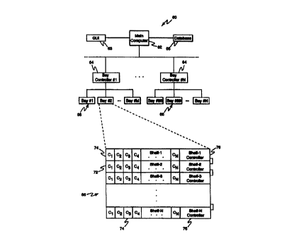
accordance with this embodiment, a central office 60 is typically organized in
a
2 5 hierarchical fashion, and includes a number of bays or frames 66, each of
which
houses several shelves ?2 of cross-connect circuits 74. A specified number of
individual cross-connect circuits 74 are removably installed in each of the
shelves 72. A shelf controller 76, also removably housed in each of the
shelves
CA 02308473 2000-OS-02
WO 99/26426 PCT/US98n4447
11
72, communicates with each of the cross-connect circuits 74 installed within
the
shelf 72.
An embodiment of a shelf 72 within which a number of individual cross-
connect circuits 74 and a shelf controller 76 are removably installed is
illustrated
in Fig. 4. A number of individual cross-connect circuits 74 may also be
grouped
to form packs 73 of circuits 74, such as four circuits 74 being grouped to
form a
modular "quad" card 73. The shelf 72 includes a printed circuit board (PCB)
backplane which provides for the communication of information and power
signals between the circuits 74 and controller 76, and provides connectivity
with
other circuits 74, shelf controllers 76, and components of the cross-connect
system 60.
Each of the shelf controllers 76 communicates with a bay controller 64
which, in turn, communicates with a main computer 62, such as a central office
computer. In one embodiment, the bay controller 64 cooperates with the main
computer 62 to coordinate the activities of the shelf controllers 76 installed
in
one or more of the bays 66. A bay controller 64 may, for example, service up
to
32 bays 66 of cross-connect equipment. In an alternative configuration, each
shelf controller 76 may communicate directly with the main computer 62. The
main computer 62 may be employed as a central information and control
2 o resource for a number of bay controllers 64 maintained at a central office
60. It
is understood that the bays 66 of cross-connect equipment constituting a
central
office may be situated at a single location, such as a building, or
distributed at a
number of geographically separated locations.
Connection information is acquired from individual shelf controllers 76
2 5 and communicated to the main computer 62, where it is stored in a cross-
connect
database 65. A graphical user interface (GUI) 63 is employed by a user to
access
the database 65. It is understood that the main computer 62 may constitute a
single computer platform or a distributed platform connected via a network or
CA 02308473 2000-OS-02
wo 99ns~26 pcrnls~
12
other communications infrastructure. The database 65 may constitute a single
non-volatile memory device or a distributed memory device.
A cross-connect system operating in accordance with the principles of the
present invention advantageously exploits TRACE wire connections as a
communications conduit for implementing various connection sensing,
identification, and monitoring functions. it is understood in the industry
that
TRACE wire or lamp wire is used in a conventional DSX system to connect the
TRACE LEDs of each of the cross-connected circuits for purposes of manually
tracing a connection. The cross-connect system of the present invention
utilizes
l0 TRACE wire and patch cord connections to effectively form scanning busses
over which scanning signals are transmitted in accordance with a unique
scanning methodology.
As will be discussed in greater detail, this unconventional use of TRACE
wire and patch cord connections within a cross-connect system, in combination
with the scanning protocol described hereinbelow, provides for the continuous
and near real-time acquisition of connection status information which is
maintained and updated in a centralized cross-connect database. It is noted
that
the term "scanning bus" as used within the context of the embodiments
disclosed
herein refers to either one or both of TRACE wire and patch cord connections.
2 0 In a general context, a scanning bus is intended to refer to any
connection,
whether electrical, optical or otherwise, within a cross-connect system other
than
a connection intended to be used exclusively for communicating information
signals.
In the embodiment shown in Fig. 5, a scanning bus or network is
2 5 illustrated which is used to communicate connection and other information
between cross-connect circuits, shelf controllers, and a main computer of the
intelligent cross-connect system. In this configuration, the scanning bus
includes
a network connection 86 over which shelf controllers 76 of a particular bay or
bays 66 communicate with each other. The network connection 86 may
CA 02308473 2000-OS-02
WO 99IZ6426 PCT/US48/24447
13
constitute an EIA-485 serial communication connection, which is understood to
be a four-conductor, mufti-drop, full-duplex balanced signal serial bus
connection.
For purposes of illustration, and not of limitation, it is assumed that a
central oiTice of a telecommunications service provider includes one-hundred
bays 66 of cross-connect equipment. Each bay 66 includes thirteen shelves 72,
with each shelf 72 housing eighty-four individual cross-connect circuits 74.
The
shelf controllers 76 installed in respective shelves 72 of each bay 66
communicate with a bay controller 64 and with a main 62 over a private
ethernet
1 o connection 92. As such, each bay controller 64 may be viewed as
constituting a
node of the central once scanning network.
The central office or main computer 62 accumulates connection
information acquired by each of the shelf controllers 76 to develop cross-
connection records for the entire central office. Each of the bay controllers
64
cooperates with their respective shelf controllers 76 to determine all hard-
wired
and patch connections established at the central office, to detect changes to
the
various connections, and to update a cross-connect database 65 accessed by the
main computer 62 on a near real-time basis, such that any connection changes
are automatically reflected in the continuously updated database. Through the
2 0 use of a graphical user interface 63, a service provider is able to query
and
display cross-connect records 65 for any circuit within the system.
A hard-wired connection may be established between a pair of circuits
housed within the same bay, such as circuits 3 and 2 of shelves 12 and 2,
respectively, of bay 1, or between circuits housed within the same bay and
shelf.
2 5 A hard-wired connection may also be established between circuits housed in
different bays, such as between circuit 3 of shelf 1, bay 1, and circuit 84 of
shelf
13, bay 99. Further, patch cord connections may be established between circuit
pairs of a common bay or of different bays, such as between circuits 84 of
shelf 1
for bays 1 and 2, respectively. It is noted that a bridging repeater may be
CA 02308473 2000-OS-02
WO 99/26426 PCTNS98~14447
14
employed within the scanning bus configuration for effecting scanning
operations between cross-connect circuits of distantly located bays.
In one embodiment, a bay controller 64 is embodied as a single board
computer or PC motherboard running an appropriate communications protocol to
effect transmission between the private ethernet 92 and the shelf controllers
76.
The ethernet protocol may be an ASN.1 compliant simple network management
protocol (SNMP) running on top of TCP/IP. Data rates ranging between
approximately 10 Mbps and 100 Mbps are obtainable using this arrangement. A
bay controller 64 communicates with a number of shelf controllers 76 using an
1 o EIA-485 bus protocol, in which the bay controller 64 operates as a single
master
which polls the shelf controllers 76. The shelf controllers 76 transmit
information only when polled by the bay controller 64.
In further discussing this embodiment, each shelf 72 is assigned a unique
48 bit ID number. During an initial system configuration phase, the bay
controller 64 retrieves the 48 bit ID of all shelves 72 connected thereto. The
bay
controller 64 then assigns each shelf an 11 bit ID number which will be used
in
subsequent communications.
Arbitration on the EIA-485 connection is facilitated by operating in a
four wire, full-duplex mode; two for transmit, and two for receive. If there
is
2 o more than one new device on a particular EIA-485 bus, as may occur at
initial
power-up, an arbitration scheme using the 48-bit shelf ID is employed to
resolve
collisions. It is noted that in an embodiment of a shelf controller that
utilizes a
universal asynchronous receiver/transmitter (DART), the UART is byte oriented
and generally must complete the current byte transmission before reacting to a
2 5 collision.
When a collision on an EIA-485 connection occurs, each node initially
uses the least significant bit of the shelf ID to resolve the collision. When
a new
device poll event occurs and bus inactivity has been verified, each node
attempts
to respond to the new device poll. If a collision occurs, the nodes stop
CA 02308473 2000-OS-02
wo ~n~26 pcros~
is
transmitting. If the shelf ID bit of a node implicated in the collision is
zero, this
node responds again immediately. The next most significant bit of the shelf ID
for this node is then pointed to for arbitrating subsequent collisions.
Otherwise,
the node awaits the next new device poll event.
Most, if not all, SNMP commands and responses between the main
computer 62, through which the cross-connect database 65 is accessed, and the
bay controllers 64 are generic queries and responses conforming to the
Management Information Base (MIB) format. The MIB is an industry standard
data format which provides for the network management of a device. Within its
1 o device-specific structure, the MIB data contains all of the information
about the
bay controller 64 and all of the associated shelf controllers 76 and alarm
collection shelves, as well as any future devices that are connected to it. A
request from the bay controller 64 typically indicates the element of the MIB
data
of interest, and the response is generally the same message with appropriate
values) added. When an event occurs, the bay controller 64 initiates an SNMP
trap. The main computer 62 then responds in an appropriate manner so that the
bay controller 64 is informed that the message was received.
Referring now to Figs. 6 and 7, there is illustrated a pair of connected
cmss-connect circuits 102, 104 in accordance with one embodiment of the
2 o present invention. In this configuration, each cross-connect circuit 102,
104
plugs into a shelf or chassis 100. Permanent equipment connections are
terminated on the rear of the shelf 100. The permanent connections established
on the rear of the shelf 100 are ei~ectively passed through the cross-connect
circuits 102, 104 to the front of the circuits 102, 104. Each piece of
equipment
2 5 may be cross-connected to other equipment components typically by
installing a
five-conductor jumper cable to terminals extending from the front of circuits
102, 104.
The five-conductor cable is an industry standard cable that is used by a
variety of cross-connect equipment suppliers. The five conductors support a
*rB
CA 02308473 2000-OS-02
wo ~n~ea,6 rcrrt~s~
16
transmit and receive pair, plus an additional TRACE conductor. In a DSX-1
configuration, this five-conductor cable constitutes a twisted pair cable that
is
"wire-wrapped" to appropriate terminal posts provided on the circuits 102,
104.
In the case of a DSX-3 system, cross-connections are established using two
coaxial jumpers for transmit and receive, along with a third jumper that
connects
the TRACE line contacts. In a fiber optic cross-connect system, a separate
electrical conductor is typically used as the TRACE conductor. Alternatively,
connection information in the form of optical signals may be communicated
along a separate fiber optic TRACE connection.
1 o When used in a conventional manner, the TRACE or "TL" connection
provides a means of manually tracing the connection between cross-connected
circuits, such as circuits 102, 104 shown in Fig. 6. By activating the TRACE
on
one circuit, such as circuit 102, through use of a switch or jack operation,
the
TRACE line is grounded, which causes TRACE LEDs 106 of the respective
circuits 102, 104 to illuminate. Illumination of the TRACE LEDs 106 of a cross-
connected circuit pair permits manual tracing of the circuits and
identification of
the cross-connected circuit locations within the central offce.
Figure 7 is a front view depiction of the circuits 102, 104 shown in Fig. 6,
and illustrates an embodiment in which a singe TRACE LED 106 is employed.
2 0 The cross-connect circuit embodied in the schematic illustration of Fig. 8
includes two TRACE LEDs 106, namely, a red and a green LED 106. The front
panel of a cross-connect circuit may additionally include a two digit, seven
segment display with incrementing momentary pushbuttons for the two digits
and a clear momentary pushbutton, all of which is controlled with firmware.
2 5 Various types of status and instructional information may be displayed to
a
technician through use of the circuit display. It is noted that firmware
residing in
a memory provided in a cross-connect circuit, shelf controller, or bay
controller
may be installed and updated by implementing an appropriate firmware
downloading procedure.
CA 02308473 2000-OS-02
WO 99/26426 PCT/US98/24447
17
It is well appreciated by those skilled in the art that the task of accurately
identifying the location and status of all cross-connected circuits within a
central
office, and updating connection records on a regular basis, represents a
significant challenge to the service provider. A telecommunications service
provider, for example, may manage over one hundred bays of cross-connect
equipment maintained at a single location, with many such installations
established in various cities. By way of further example, a single central
office
location which houses one hundred bays containing thirteen shelves within
which eighty-four cross-connect circuits are installed provides for a total of
109,200 connections established at this single location.
Maintaining accurate connection records for hundreds of thousands of
connections has proven to be impractical, if not impossible, using
conventional
manual tracing approaches. The cross-connect monitoring system of the present
invention provides for accurate and continuous electronic monitoring and
updating of connection records for any number of connections.
Figure 8 is a schematic representation of the MONITOR, OUTPUT, and
INPUT bantam jacks 108, 110, 112 and ancillary circuits shown in Fig. 7. A
partial showing of a typical bantam plug 120, which is connected to each of
the
opposing ends of a patch cord, is shown in Fig. 9. The normal function of a
2 0 patch cord when used within a cross-connect system is to temporarily re-
direct a
circuit connection to a termination point different from that established by
the
circuit's hard-wired connection.
As can be seen in Fig. 8, when a bantam plug 120 of a patch cord is
inserted into either the OUTPUT jack 110 or INPUT jack 112 of a cross-connect
2 5 circuit 102, the circuit connection to the hard-wired connection is
broken, such
that a new conductivity path is established over the patch cord. The bantam
plug
120 connected at the opposing end of the patch cord may then be inserted into
an
appropriate OUTPUT or INPUT jack 110, 112 of another cross-connect circuit
CA 02308473 2000-OS-02
wo ~n~z6 pcrius9sn~~
is
104, thereby establishing a new and generally temporary cross-connection
through the patch cord.
A conventional bantam plug 120 used in the industry for establishing
patch connections typically includes three conductors which are identified in
telephony ternis as TIP, RING, and SLEEVE (i.e. SHIELD). The TIP and
RING conductors are used to transmit information signals, while the SLEEVE or
SHIELD is used as an interference protection mechanism (e.g., ground shield).
As can be seen in Fig. 8, when a bantam plug 120 is inserted into either the
OUT
or IN jack 110, 112, the respective OUT or IN signal will redirected over the
patch cord, and the connection to the TN/RN wired cross-connect 122 will be
broken. It is noted that the TL, TR, and RN signal contacts 122 represent hard-
wired (e.g., wire-wrapped) connections, and the IN/OUT R, T connections 124
represent the rear permanent connections.
Referring now to Figs 10-12, there is depicted an embodiment of various
circuit elements which are used in an intelligent digital cmss-connect system
to
electronically and automatically identify and monitor all connections
established
through the circuits of the cross-connect system on a continuous basis. In
accordance with this embodiment, and as discussed briefly hereinabove, the
TRACE wire conductor 133 is utilized in an unconventional manner, in that a
2 0 scanning signal is communicated through the TRACE wire conductor 133 in
accordance with a unique cross-connect scanning methodology.
In broad and general terms, a shelf controller 136 generates a scanning
signal, which includes location identification information associated with a
tn~nsmitting cross-connect circuit 132, and transmits the scanning signal
across
2 5 the TRACE wire conductor 133 of the transmitting circuit 132. The scanning
signal communicated by the transmitting cross-connect circuit 132 is received
by
a receiving cross-connect circuit 134. Having received that scanning signal at
the circuit 134, the shelf controller 136 associated with the receiving
circuit 134
reports the transmitting and receiving circuit location identification
information
*rB
CA 02308473 2000-OS-02
wo ~r~c~Z6 rcrms9sn~~
19
to a main computer, such as the bay controller 64 or main computer 62 shown in
Fig. 3. It is understood that the receiving circuit 134 may be located in the
same
shelf 130 as the transmitting circuit 132, a dii~erent shelf 130 within the
same
bay, or a shelf of a bay distantly located from that housing the transmitting
circuit 132.
The shelf controller 136 dedicates an individual connection for each
TRACE connection of individual cross-connect circuits installed in a
particular
shelf 130. Each shelf controller 136 transmits circuit location identification
information, typically by use of a digital scanning signal, across each of its
TRACE wire connections either in a particular sequence or in parallel
depending
on the particular scanning algorithm employed. By transmitting a location
identification signal on one port and receiving a location information signal
on
another port, the shelf controllers 136 of a cross-connect system collectively
identify the location of all circuits established through the cross-connect
system.
Unused circuits are also identified. All shelf controllers 136 in all
equipment
bays proceed through this general scanning operation in order to identify all
of
their respective connections. Each shelf controller 136 will then report its
connection information to a main computer 64 via a data connection.
Concerning the circuit configuration shown in Fig. 12, and as briefly
2 0 discussed hereinabove, a patch cord 143 may be employed to temporarily re-
direct informatian signals between cross-connect circuits other than those
connected through use of a hard-wired connection. When the bantam plug of a
patch cord in sensed in either the IN or OUT jack 112, 110, a scanning signal
produced by the shelf controller 136 is transmitted over the SLEEVE or SHIELD
2 5 conductor of the patch cord 143 to a newly selected receiving cross-select
circuit
134. Information identifying the location of the transmitting circuit 132 is
encoded in the scanning signal and used together with information identifying
the selected receiving circuit 134 to identify the newly established patch
connection. This information is similarly communicated to a central computer.
CA 02308473 2000-OS-02
WO 99/26426 PCTIUS98/24447
Using the SLEEVE or SHIELD conductor of the patch cord 143
advantageously provides a conduit for communicating scanning signal
information without requiring additional patch cord conductors. It is
understood
that modifying the configuration of an industry standard patch cable so as to
5 include an additional conductor would result in increased costs and the
potential
of making obsolete hundreds of thousands of cross-connect patch cables
currently in use. Because the transmission speed of the scanning data is
relatively low, no appreciable interference problems arise with the use of the
shield conductor of the patch cord 143.
to A generalized system block diagram of a shelf controller 150 is depicted
in Fig. 13. In accordance with this embodiment, the shelf controller 150
includes
a micro-controller I52 which communicates with a memory 154 and various
digital devices 158, 160, 162 over a data bus 164. The general function of the
digital interface circuits 158, 160, 162 is to receive or transmit data from a
large
15 number of input/output sources and, when requested, present this data to
the
micro-controller's data bus 164. The micro-controller 152 then stores all of
the
connection and status information into the memory 154, and when requested,
transmits this information over the serial data bus 168 to the main computer.
The micm-controller 152 communicates with an ancillary processor, such as a
2 o bay controller 64, thmugh serial data transceiver circuits 156.
A digital interface circuit 158, which is coupled to a number of jack sense
lines, receives signals indicating the presence or absence of a bantam plug in
any
one of the MONITOR jack 108, the OUTPUT jack 110, or the INPUT jack 112.
A digital interface device 162 communicates with a TRACE LED 106 and
2 5 controls the illumination, flashing, color selection, and other operations
of the
TRACE LED 106. Using the jack sense lines to sense the presence of a bantam
plug in the MONITOR jack 108, the shelf controller 150 may activate the
TRACE LEDs 106 for a pair of connected circuits so as to simulate a "trace" as
would otherwise occur within a conventional cross-connect systems.
CA 02308473 2000-OS-02
wo ~n~z6 pcrms~
21
In general, the scanning signal tzansmitted through a TRACE connection
or patch connection provides location identification and status information
regarding the transmitting cross-connect circuit. In Table 1 below, there is
provided various types of information that may be encoded in a scanning signal
in accordance with one embodiment of the present invention.
CA 02308473 2000-OS-02
WO 99/Z6426 PCT/US98/24447
22
TABLE 1
.,
Shelf Number ~ 11 or more bits
Circuit Number 7 or more bits
Path Number 2 bits
Command 8 bits
Checksum 8 or more bits
Synchronizing Bits 2/8 bits
Start/Sto
In one embodiment, the identification of the shelf number and cross-
connect circuit number are encoded using eleven and seven bits, respectively,
irrespective of whether the scanning signal is transmitted over a TRACE wire
connection or patch connection. The Path Number field indicates the
transmission path as being either the TRACE, Patch IN, or Patch OUT
connection. It is to be understood that the scanning signal fields provided in
l0 Table 1 represents a non-exhaustive list of information variables which may
be
encoded in a scanning signal. Other information different from or in addition
to
that included in Table 1 may also be encoded in the scanning signal.
Each of the shelf controllers maintains a local database of identification
and status information concerning the cross-connect circuits with which it
communicates. Table 2 below provides an example of various types of
information which may be maintained and updated in the local database of a
shelf controller.
CA 02308473 2000-OS-02
WO 99/26426 PCT/US98/24447
23
TABLE 2
I '~~
. :,~> ;
. Full Shelf Number 48 bits
Abbreviated Shelf Number 11 bits
Circuit Parameters: (Number of bits x Number
of
'TRACE -wired Circuit ID circuits)
Circuit Number 7 bits
Path Number 2 bits
Patch tem Circuit ID
Circuit Number 7 bits
Path Number 2 bits
MONITOR Jack Occ ied 1 bit
Patch IN Jack Occu ied 1 bit
Patch OUT Jack Occ ied I bit
LED State 4 bits
Red LED OK 1 bit
Green LED OK 1 bit
Circuit Pack Present 1 bit
The four LED bits provide for four LED states, including OFF for both
Red and Green LEDs. Combining these states provides the opportunity to use
yellow or orange, depending on the current limiting resistors chosen. The LEDs
may change state every eighth of a second allowing for a variety of LED
presentations to be implemented.
As was discussed previously, the scanning signals which are received by
a receiving cross-connect circuit are communicated to a main computer and
preferably stored in a database containing cross-connect information. An
exemplary set of database fields for such a database is provided below in
Table
3. In general, the cross-connect database provides for the storage and access
of a
comprehensive set of information concerning each and every cross-connection
established through a central once.
In accordance with one embodiment, the database includes fields
generally corresponding to those associated with the information provided in
CA 02308473 2000-OS-02
wo ~n~a~ rcrms9sn444~
24
Tables 1 and 2 above, as well as other information of interest, such as the
central
office location, name, floor, and location of a particular bay, connection
history,
and user or administrator comments, for example.
TABLE 3
~, i I ~
Ci a i~ ~ I
~ ~'~ r~' ~i~~i~ ~~~~~~!~6I'~V'~ ~ ' ',~
II~
Name of the Ci
Central O~ce Name of the Central Office/Exchan a
Floor Floor Location of the Cross-Connect Ba
Ba No/Name Ba /Frame Name
Shelf No. Shelf Number
Circuit No. Circuit Number or Port within Shelf
CLLI Name Common a Location Identifier
Circuit Type Identifies whether Circuit Port is a "Facility
Side", or
"Network Side" Port
Circuit Descri Free-Format Descri tion Field for the
tion Customer
Connection StatusIdentifies whether the Port is Connected
or not Connected
Connection HistoryProvides a History of Connection Status
Information -
Including Time/Date Stamp, Circuits Connections
and
Disconnections
Comments Free-Format Comment Field with USER ID,
Date/Time
Stam
Cross-Connect Fields of Detailed Connection Information
Information
One of several functions performed by the shelf controller 150 involves
detecting a change in the condition of a patch cord, such as whether any patch
1 o cords have been installed into or removed from a particular jack of a
particular
cross-connect circuit. As can be best seen in Fig. 8, additional el~trical
contacts
within each of the MONITOR, OUTPUT, and INPUT jacks 108, 110, 112
provide an indication to the shelf controller 150 as to the status of these
jacks
(i.e., bantam plug present or absent). All of the jack sense lines ate
connected
via the backplane of a shelf chassis to the shelf controller 150. The micro-
controller 152 periodically polls the status of each of the bantam jacks,
stores the
CA 02308473 2000-OS-02
WO 99/26426 PCTJUS98n4447
status information in the memory 154, and reports this information to the main
computer when requested.
In general, when the main computer issues a command instructing a
selected shelf controller to activate the TRACE LED of a particular circuit,
the
5 shelf controller causes the appropriate circuit LED to illuminate according
to a
pre-established flash pattern. It is noted that a flash pattern refers to a
LED flash
program that indicates various LED illumination parameters, such as steady
and/or flash durations, flash speed, single or multiple colors usage, and
other
LED operating parameters. The TRACE LED will typically remain illuminated
10 until the shelf controller receives an instruction from the main computer
to taro
off the TRACE LED or until such time as a flash pattern timer expires. The
main computer may also initiate a command instructing a selected shelf
controller to cause the TRACE LED of a particular circuit to flash. The shelf
controller may store FLASH-ON and FLASH-OFF timing information, and will
15 typically cause a TRACE LED to continue flashing at a specified rate until
it is
requested to terminate the flashing operation.
One particular function that is implemented through execution of the
TRACE LED control and jack sense procedures, as mentioned previously, is the
simulation of an industry-standard "trace" operation. Such an operation
typically
2 o involves placing a bantam plug into the MONITOR jack of a particular
circuit to
initiate the trace. In a standard digital cross-connect system, this would
result in
grounding of the TRACE wire, thereby causing the TRACE LEDs at both ends
of the circuit connection to illuminate.
In accordance with the present invention, however, insertion of the
2 5 bantam plug in the MONFTOR jack is sensed by the shelf controller 150
which,
in response, transmits an LED flash command over the scanning bus. The LED
flash command is decoded by the shelf controller associated with the receiving
partner circuit which causes the LED(s) of the partner circuit to illuminate
in
accordance with a selected flash pattern.
CA 02308473 2000-OS-02
WO 991Z64Z6 PCT/US98/24447
26
A more detailed description of various process steps associated with
controlling the TRACE LEDs during a trace operation is shown in Figs. 14 and
15. The shelf controller initiates 20(? a TRACE simulation procedure by
selecting 202 a first circuit installed within the shelf. If an LED flash
command
issued by the main computer has been previously transmitted 204 with respect
to
the selected circuit, the shelf controller detects this activity and selects
206
another cross-connect circuit in the shelf. If an LED flash command has not
been issued, the shelf controller senses 212 the MONITOR jack of the selected
circuit.
1 o If a bantam plug is detected in the MONITOR jack, and if the flash
pattern for the selected circuit is not currently active 216, the flash
pattern
function for the selected cross-connect circuit is initiated 218 and the flash
pattern timer is turned on. If the MONTTOR jack is occupied 212 and the flash
pattern is already active 216, the TRACE LED 106 for the selected circuit is
set
222 to a steady ON state if the flash pattern timer has expired 220. If the
flash
pattern timer has not expired 220, the shelf controller selects 206 another
cross-
connect circuit of the shelf.
If a flash command for the selected circuit is not active 204, and the
MONITOR jack of the selected circuit is not occupied 212, the flash pattern
2 0 operation is halted, and the shelf controller selects 206 another cross-
connect
circuit of the shelf. The TRACE simulation procedure continues until all of
tire
cross-connect circuits of the shelf have been monitored 208, 210.
Additional TRACE LED control steps are depicted in Fig. 15. The shelf
controller senses 230 the status of the MONITOR jack of all circuits with
which
2 5 it communicates. This monitoring process continues until such time as a
FLASH
command is received 232 from the main computer. If the command received
238 from the main computer is not a CLEAR LED instruction, then the shelf
controller initiates 242 an LED flash procedure for the indicated cross-
connect
circuits with the indicated illumination pattern.
CA 02308473 2000-OS-02
WO 99/26426 PCT/US98124447
27
If active, the flash pattern is overridden 244 under this condition. If the
flash command received 232 from the main computer is a CLEAR LED
instruction 238, and if the flash pattern function is in a flash or steady on
state
236, the LED flash is cleared and the flash pattern function is restored for
the
indicated cross-connect circuit. If the locate function is not in a flash or
steady
on state 236, then the LED is turned off 234.
It can be appreciated that the cooperative operation between the shelf
controller and the main computer provides the opportunity to erect a full
range
of control over the TRACE LEDs for a variety of purposes. It is noted that one
1 o or more LEDs of a cross-connect circuit may be controlled by the shelf
controller, and that the LEDs may be monochromatic or multi-chromatic in type.
By way of example, cooperation between the shelf controller and main computer
provides the ability to effectively guide a technician through various patch
connection or disconnection operations.
In one embodiment, a "patch pending" file is created which indicates
various connections or disconnections to be effected by a technician to
accomplish a particular objective. The patch pending file, when executed by
the
main computer, may control multi-colored TRACE LEDs of specified circuits as
a means of visually directing the work of a technician when establishing and
2 0 breaking cross-connections. A flashing green LED indication, for example,
may
identify circuits in which a patch cord is to be inserted, while a flashing
red LED
indication may identify circuits in which an existing patch cord is to be
removed.
A patch pending file typically contains information identifying the
specific sequence by which patch cord installation or removal is to be
2 5 accomplished by a technician. The main computer then steps a technician
through each change, one circuit pair at a time. Since the main computer knows
precisely when and where a patch cord is to be inserted or removed, the
implicated LEDs may continue to flash until the technician effects a proper
connection or disconnection for a particular circuit.
CA 02308473 2000-OS-02
WO 99/Z6426 PCT/US~24447
28
By way of fiuther example, a patch pending file may be created which
provides information concerning contingent or back-up connections that may be
established in the event of a network outage. In a large communications
network
with critical circuits, for example, a patch pending file may identify
important
circuits which require immediate restoration during temporary or extended
outages. When a system outage occurs within a typical central office,
technicians typically use a shot-gun approach when attempting to identify all
cross-connected circuits affected by the outage and the location of temporary
patches that must be effected in order to restore important circuit
connections.
Creation of a patch pending file well in advance of an outage situation,
provides
an opportunity for the service provider to develop a well-considered strategy
for
dealing with any number of potential outage scenarios.
Upon occurrence of an actual system outage, an appropriate patch
pending file may be selected and executed to implement an efficient,
coordinated
patching procedure for restoring key circuits. On-site technicians may then
quickly proceed through the cross-connect system guided by the LED patch
sequencing process in their effort to patch and unpatch specified circuit
connections. It can be appreciated that use of patch pending files in this
manner
saves precious time in restoring important and other circuits impacted by an
2 0 . outage, which would otherwise be wasted on looking up records and
sorting out
needed connection information under stressful conditions associated with a
major outage.
Referring now to Figs. 16A-27, there is depicted various embodiments of
a scanning methodology and apparatus by which all connections established
2 5 through a cross-connect system or central office may be identified, and
status
information acquired and updated for all connections on a continuous basis. To
facilitate an understanding of the various scanning approaches, reference is
made
to the circuit 600 depicted in Fig. 16A. The circuit 600 is typically
incorporated
as part of the shelf controller and may be embodied in a micro-controller, an
CA 02308473 2000-OS-02
WO 99/Z6426 PCT/US98~14447
29
Application Specific Integrated Circuit (ASIC) or Field Programmable Gate
Array (FPGA), for example.
The circuit 600 includes a number of receive registers 602 and transmit
registers 604 associated with each cross-connect circuit coupled to the shelf
controller. In a shelf configuration in which 84 cross-connect circuits are
housed, for example, the circuit 600 will include 84 receive register sets 608
and
84 transmit register sets 618, one receiver and transmit register set 608, 618
being respectively associated with each of the 84 cross-connect circuits.
The particular configuration of the circuit 600 may be varied to
accommodate a variety of processing, speed, synchronization, and ASIC/FPGA
floor planning (i.e., circuit layout) considen~tions. By way of example, each
receive and transmit register set 608, 618 respectively includes a TRACE
register
610, 620, a Patch IN register 612, 622, and a Patch OUT register 614, 624. In
the embodiment illustrated in Fig. 16A, each of the TRACE, Patch IN, and Patch
OUT registers constitutes a First-In-First-Out (FIFO) register or stack, it
being
understood that other butl'ering or memory implementations may be employed.
In one embodiment, the TRACE, Patch IN, and Patch OUT FIFOs 610,
612, 614 associated with the receive register 602 may each be coupled to a
respective receiver circuit (not shown), and the TRACE, Patch IN, and Patch
2 o OUT FIFOs 620, 622, 624 associated with the transmit register 604 may each
be
coupled to a respective transmitter circuit (not shown). In this
configuration,
each cross-connect circuit is thus provided with three transmitters and three
receivers. As such, data may be transmitted from and received by the three
dedicated receive and transmit FIFO sets in a simultaneous or parallel manner.
2 5 Figure 16B is generally illustrative of this particular embodiment.
In an alternative embodiment, a single receiver may be multiplexed
across the TRACE, Patch IN, and Patch OUT FIFOs 610, 612, 614 associated
with each cross-connect circuit, and a single transmitter may be multiplexed
across the TRACE, Patch IN, and Patch OUT FIFOs 620, 622, 624. Another
CA 02308473 2000-OS-02
WO 99/26426 PCT/US98/24447
alternative configuration, by way of fiuther example, includes a single
multiplexed transmitter and three dedicated receivers. It is appreciated that
use
of a multiplexed transmitter requires some form of sequential or selective
circuit
path switching amongst the associated transmit FIFOs.
5 In accordance with a particular circuit 600 embodiment, as is illustrated
in Fig. 16C, a single ASIC provides all of the logic required to support 16
cross-
connect circuits. The number of cross-connect circuits supported in a
particular
shelf configuration may be expanded simply be installing additional ASICs.
Each sub-circuit of an ASIC, such as Circuit #1 or Circuit #N shown in Fig.
16A,
10 includes three physical pins respectively dedicated to the three circuit
paths (i.e.,
TRACE, Patch IN, Patch OUT). Internally, the receive and transmit logic for
each pin is functionally OR tied.
For purposes of increasing design flexibility and processing speed, the
ASIC includes three transmitters and three receivers for each sub-circuit so
as to
15 provide for simultaneous data transmission and reception. The pins of the
ASIC
coupled to each cross-connect circuit include the following: TRACE Bus; Patch
IN Bus; Patch OUT Bus; MONTfOR Jack Occupied; IN Jack Occupied; OUT
Jack Occupied; Red LED; Green LED; and Circuit Pack Present pins. It is noted
that a Circuit Pack Present signal received at the Circuit Pack Present pin
2 0 indicates the presence of particular grouping or pack of cross-connect
circuits
within the shelf. The ASIC also includes a number of standard pins, such as
data
bus, address bus; CLK, and other control signal pins.
A central processing unit (CPU) or micro-controller of the shelf
controller cooperates with the circuit 600 to coordinate the operation of the
2 5 receive and transmit register 602, 604. The receive and transmit FIFOs
602, 604
of a particular cross-connect circuit are employed to store data pertaining to
the
connection established between the particular circuit and the circuit
connected
thereto, and to effect the various scanning procedures implemented in
accordance with the principles of the present invention.
CA 02308473 2000-OS-02
wo ~n~a26 rcrms9~
31
In accordance with a general scanning methodology, each cross-connect
circuit h~ansmits its unique identification (1D) information or code to a
partner
circuit connected thereto. The partner circuit receiving the transmitting
circuit's
ID code stores this data and, when requested by the bay controller or main
computer, transmits the transmitting circuit ID code and its own ID code to
the
main computer. Other connection status information may also be communicated
between the transmitting and receiving circuits and transmitted to the main
computer.
It can be appreciated that only the receiving circuits need transmit their
respective connection information to the main computer in order to obtain the
identification of all cross-connected circuit pairs within the system. It is
important to note that the transmitting side generally does not know of the
status
of the receiving side. A transmitting circuit, therefore, will continue to
transmit
at regular intervals, thus providing a keep-alive signal to the receiving
partner
circuit. Moreover, after acquiring an initial set of connection information
from
all receiving circuits, only those receiving circuits containing new
connection or
disconnection information need pass the information to the bay controller or
main computer.
In one embodiment, as will be discussed in detail hereinbelow, all circuit
2 0 connections will be scanned and identified within the time it takes to
transmit a
single cross-connect circuit ID bit string, irrespective of the size of the
cross-
connect system (i.e., number of cross-connect circuits). If, for example, it
is
assumed that a given scanning methodology employs a circuit ID code of n bits
in length, that startJstop and stut~ bits constitute m bits, and that the
clock speed
2 5 is given as CLK Hertz, then the total scan time required to identify all
circuit
connections is given by:
(n + m)~(1/CLK)
CA 02308473 2000-OS-02
WO 99/26426 PCTNS98/~4447
32
In stark contrast to conventional schemes in which the time required to
identify all connections established within a cross-connect system increases
as a
function of increasing circuit population, the time required to identify all
cross-
connected circuits using the scanning approach depicted in Figs. 17-23C is
relatively short and constant (e.g., 100 - 500 milliseconds), regardless of
whether
the system contains ten thousand, one-hundred thousand, or even a million
cross-
connected circuits.
In the following discussion, reference will be made to a Transmit Table
in connection with various procedures of a scanning operation. The circuit 600
depicted in Fig. 16A represents one conceptual embodiment of a Transmit Table,
it being understood that other implementation may be employed in hardware and
software to facilitate the scanning methodology. Initially, the Tran~nit Table
is
established in which circuit ID and patch status information is loaded for
each of
the circuits coupled to a respective shelf controller of the cross-connect
system.
The loading function, such as that depicted in Figs. 17-18, takes into
consideration all hard-wired connections between circuit pairs, and,
importantly,
all patch connections established using patch cords connected to the IN/OUT
jacks of the circuits. As such, all physical cross-connections, whether hard-
wired
or patch connections, are identified.
2 0 A typical Transmit Table loading open~tion is initiated upon receiving
300 a broadcast command issued from the main computer. After receiving the
broadcast command, each of the transmit TRACE FIFOs 620 of each cross-
connect circuit within a shelf is loaded with a TRACE identification code
(TRACE ID). The TRACE ID represents a code which uniquely identifies the
2 5 TRACE jack of a particular cross-connect circuit. In a similar manner,
Patch IN
and Patch OUT IDs represent codes which uniquely identify the Patch 1N and
Patch OUT jacks of a particular cross-connect circuit. The loading procedure
illustrated in Figs. 17-18 is implemented by each shelf controller for all
bays of
cross-connect equipment in a contemporaneous, parallel manner.
CA 02308473 2000-OS-02
wo ~r~ta.6 rcrms9sr~a4~
33
In addition to loading TRACE ID information into respective transmit
FIFOs, the shelf controller scans 304 each of the circuit receive register 602
to
determine 306 if a circuit ID currently resides in the circuit's receive TRACE
FIFO 610. If a valid circuit ID is stored in the receive TRACE FIFO 610 for a
particular circuit, the )D of the partner circuit has been previously
received. As
such, the identity of the cross-connected circuits is already known, and the
scanning operation need not be repeated 308 for this circuit connection.
Although not required, it may be desirable to perform a re-scan operation for
the
particular circuit connection.
1 o If a circuit ID is not currently stored in the receiver TRACE FIFO 610 for
a selected circuit, the shelf controller determines whether a patch cord has
been
inserted into either of the Patch IN or Patch OUT jacks. In particular, if a
circuit
ID is not currently residing 310 in the receive Patch IN FIFO 612 for the
selected
circuit, the shelf controller determines 312 whether the Patch IN jack is
occupied, and if so, adds 314 the Patch IN ID to the transmit patch IN FIFO
622
of the Transmit Table for the selected circuit.
If a valid circuit ID currently resides in the receive Patch OUT FIFO 614
for the selected circuit, the ID of the partner circuit has previously been
received
and the scanning operation need not be repeated for this circuit connection,
2 0 although it may prove desirable to re-scan the circuit connection. If not,
the
Patch OUT jack is sensed 318, and if occupied, the shelf controller adds 320
the
Patch OUT ID to the transmit patch OUT FIFO 624 of the Transmit Table for the
selected circuit. All circuits coupled to the shelf controller are similarly
processed 322. After processing all of the respective circuits associated with
the
2 5 shelf controller, the scanning procedure generally depicted in Fig. 19 is
initiated
324. The shelf controller reports 326 completion of the scanning procedure 324
to the main computer upon completion.
It is to be understood that the general principles of the scanning approach
described herein may be implemented in a manner which does not require
CA 02308473 2000-OS-02
WO 99126426 PCT/US98/24447
34
interaction with a Transmit Table of the type previously described, but that
the
description of such a Transmit Table is provided for illustrating one of
several
approaches for implementing the present invention. Having completed the
Transmit Table loading procedure depicted in Figs. 17-18, the scanning
procedure depicted in Fig. 19 is initiated by all shelf controllers in a
contemporaneous, parallel manner.
In accordance with this procedure, all circuits within the cross-connect
system transmit their respective full circuit ID codes according to the
procedure
illustrated in Fig. 19. In particular, all shelf controllers transmit ID and
other
information for those circuits having circuit ID codes currently loaded in the
Transmit Table. These transmissions can take place over several circuit paths
simultaneously, such as over the TRACE conductor or the Patch IN and OUT
conductors.
Collisions are resolved using the approach depicted in Figs. 20-23C. To
reiterate a significant advantage realized through employment of the instant
scanning technique, all circuit connections are scanned and identified within
the
time it takes to transmit a single cross-connect circuit ID bit string,
regardless of
number of circuits utilized within the cross-connect system.
A "listen before transmitting" approach is employed during the scanning
2 0 operation in an attempt to minimize collisions and transmissions across
the
scanning bus. If a transmission is detected on a connection coupled to a
particular circuit identified in the Transmit Table, the transmitting circuit
is
prevented from making further transmissions and its ID is removed from the
appropriate transmit FIFO 618 of the Transmit Table. In this situation, the
2 5 incoming transmission is typically, if not exclusively, a circuit ID being
communicated from a partner (i.e., cross-connected) circuit.
Because the circuit IDs for the pair of cross-connected circuits is known
by referencing the appropriate receive FIFO 608 of the receiving circuit, no
further duplicative scanning need occur for this transmitting circuit. Such
CA 02308473 2000-OS-02
wo ~n~~ t~rrt~s9sn~t~
duplicative scanning, however, will advantageously result in the repetitive
transmitting of a keep-alive signal to the receiver, as was previously
mentioned.
For those circuits in which transmission activity is not detected, the shelf
controller instructs all such circuits to begin transmitting their resp~tive
Ills
5 according to the procedure depicted in Fig. 19.
When a collision is detected on a particular circuit connection, a collision
arbitration procedure is initiated whereby one of the two transmitting
circuits
(identified as a "transmitter") is permitted to continue transmitting its full
ID,
and the other circuit is instructed to cease its transmission. This circuit's
ID is
1 o removed from the Transmit Table, and the circuit is identified as a
"receiver" for
subsequent transmissions, although it may be desirable to reset all circuits
to
"rransinitters" and repeat the collision arbitration procedure for each
subsequent
transmission.
It will be appreciated that no further collisions will occur over the
s 5 connection established between these two circuits, assuming that no change
in
hard-wired or patch connectivity occurs, because only one of the two circuits
(i.e., the transmitter circuit) is permitted to transmit its circuit ID and
other
information during subsequent scanning operations. The receiver circuit, which
has been instructed by the shelf controller not to transmit its ID over the
present
2 0 connection during subsequent scans, receives and stores the transmitter
circuit's
ID, and, when instructed, communicates this ID information and its own ID
information to the main computer.
Any change in hard-wired or patch connectivity with respect to a
particular circuit, regardless of whether the circuit is identified as a
transmitter or
2 5 receiver, is detected by the shelf controller. In such a case, the new
connection
will be scanned in the same manner as those associated with circuits
previously
loaded in the Transmit Table. In this case, the implicated circuits lose their
respective "transmitter" or "receiver" identifications. As such, any
modification
to an existing connection or addition of a new connection will be detected and
CA 02308473 2000-OS-02
WO 991Z64Z6 PCTNS98/24447
36
identified within a subsequent single scanning period (i.e., the time it takes
to
transmit a single cross-connect circuit ID bit string).
Referring to Fig. 19, the circuit ID transmission and collision arbitration
steps in accordance with the first embodiment of a scanning methodology will
now be described in greater detail. Figures 20-21B will also be referral to in
this
discussion. Figure 20 is an illustration of two cmss-connected circuits each
including respective transmit (XMIT) and receive (RCV) FIFOs 381, 389 and
383, 391 coupled to respective collision detection circuits 385, 387. The pair
of
circuits A and B are connected via an information signal connection (not
shown)
1 o and a TRACE bus connection 393. Figures 21 A, 21 B depict in table form
the
state of the xiVilT and RCV FIFOs 381, 383, 389, 391 of circuits A and B when
simultaneously transmitting circuit ID information over the TRACE bus
connection 393.
Figures 21 A, 21 B also indicate the occurrence and resolution of a
collision in accordance with one embodiment of a collision arbitration scheme
which utilizes the circuit 395 illustrated in Fig. 22. It is understood that
the
receiver/transmitter circuit 395 shown in Fig. 22 may be used in either a
dedicated mode or a multiplexed mode of operation. In a dedicated mode, a
receiver/transmitter circuit 395 is connected to each of the TRACE, Patch IN,
2 0 and Patch OUT connections (i.e., three individual circuits 395). In a
multiplexed
mode, a single receiver/transmitter circuit 395 is selectively connected to
any of
the TRACE, Patch IN, and Patch OUT connections.
A timing diagram which characterizes the operation of the
receiver/hansrnitter circuit 395 is provided in Figs. 23A-23C. The circuit
shown
2 5 in Fig. 22 constitutes a tri-state, open collector, digital transceiver,
where the
active state is represented by a logic 0 (e.g., ground), and an openlinactive
state
is represented by a logical 1 (e.g., V~).
If the cross-connect circuits at both ends of a TRACE bus connection
transmit the same signal {i.e., a 1 or 0), then no difference between the
CA 02308473 2000-OS-02
WO 99/264216 PGT/US98J~4447
37
transmitted and received sisals is detected by the collision detection circuit
395,
and a collision is deemed not to have occurred. However, if bath circuits
transmit opposite signals, a collision will be deemed to have occurned by one
of
the circuits. The cross-connect circuit transmitting the logic "0" will be
given
priority and is permitted to continue transmitting its ID code, while the
partner
circuit will detect a signal mismatch or collision condition and is prevented
from
further broadcasting its ID code. Transmitting a logic "0" overrides the state
of
the bus and pulls the bus "low."
It is noted that the receiver 397 of the collision detection circuit 395 is
1 o active during times when the transmitter 399 is inactive (i.e., times t,,
t2, t3, td, . .
.tn). During the time in which the receiver 397 is active, such as time
duration t~
for example, the receiver 397 monitors the TRACE bus connection 393 in order
to detect the presence of a transmission thereover. The receiver 397 typically
samples the TRACE bus connection 393 repetitively during each time period of
transmitter inactivity. In this manner, a listen before transmit approach to
effecting communications between cross-connected circuits is realized.
As was discussed previously, all circuits having IDs loaded in the
Transmit Table (i.e., a circuit's transmit FIFO 620, 622, or 624) for all
shelves
within the cross-connect system begin transmitting 370 their respective IDs in
2 0 parallel. In particular, each circuit transmits 371 its ID information one
bit at a
time from its associated transmitter FIFO 618. For example, and with reference
to Figs. 21A, 21B, if both circuits A and B transmit 371 a logic 1 as the
first bit
of their respective IDs from their respective transmit FIFOs 381, 389, and
both
circuits A and B receive 372 a logic 1 bit in their respective receive FIFOs
383,
2 5 393, no dii~erence between the transmitted and received signals is
detected 373
by the collision detection circuits 385, 387. As such, no collision is deemed
to
have occurred. The same result occurs when both circuits A and B transmit 371
a logic 0 as the second bit of their respective IDs. Subsequent 1D bits
transmitted
by circuits A and B are similarly tested 374, 375.
CA 02308473 2000-OS-02
wo ~r~~az6 rcrnrs9sra~e~
38
Because each circuit ID with a cross-connect system is unique, a collision
will eventually occur on the TRACE bus connection 393 coupling circuits A and
B during the scanning operation. For example, if circuit A transmits 3? 1 a
logic
0 as the third bit of its ID and circuit B transmits 371 a logic 1 as the
third bit if
its ID, a mismatch between transmitted and received ID signals is detected by
the
collision detection circuit 387. In accordance with the collision arbitration
scheme of this embodiment, the circuit transmitting a logic 0 is given
priority
(i.e., overrides the bus state) over the circuit transmitting a logic 1.
As such, circuit A is permitted to continue transmitting its 1D
undisturbed. Circuit B, on the other hand, is instructed to halt all
subsequent ID
transmissions during the existence of the present connection (i.e., no change
in
hard-wired or patch connection status), and is thereafter identified as a
"receiver"
circuit. It is noted that circuit A continues to operate as a "transmitter"
circuit
during the current and subsequent scanning operations, although no formal
procedure to identify same is required.
Importantly, the circuit ID bit information stored in the "receiver" circuit,
which in this illustrative example is circuit B, precisely corresponds to the
circuit
ID bit information transmitted by the "transmitter" circuit, in this case
circuit A.
Since only the receiver circuit reports circuit ID information for both
2 0 transmitting and receiving circuits to the main computer, it is
significant that the
collision arbitration scheme of the instant scanning methodology is non-
destructive, and ensures that the transmitting circuit ID and related
information is
received with 100% integrity.
As was previously mentioned, no further collisions will occur over the
2 5 TRACE bus connection established between circuits A and B, assuming that
no
change in hard-wired or patch connectivity occurs, because only the
tt~ansmitter
circuit is permitted to transmit its circuit ID and other information during
subsequent scanning operations. Using this scheme, all circuit connections
will
CA 02308473 2000-OS-02
wo 99ns4~s rcrnrs~
39
be known within the time it takes to transmit a single circuit ID bit string,
regardless of the size of the cross-connect system.
Under nominal operating conditions, there is generally no need for a
receiving circuit to ever transmit its ID information as long as the present
connection is maintained. In the special case where a pair of patch cords have
been incorrectly patched to different circuits, there exists the possibility
that two
simultaneous circuit IDs raay be received on the two patch paths connected to
the common circuit. In a configuration in which a single receiver of the shelf
controller is multiplexed across the three circuit paths of the circuit,
namely the
TRACE, Patch IN, and Patch OUT paths, such a misconnection condition may
be detected and remedied automatically by the shelf controller. In such a
case,
the shelf controller detects that there is a communications error on both the
Patch
IN and Patch OUT paths.
In response, the shelf controller switches the receiver multiplexer to
I 5 connect with one of the two patch paths, and waits for the next circuit ID
to
arrive. Diu~ing the ensuing dead time, the shelf controller then transmits the
selected patch path's circuit ID, so as to cause the partner circuit at the
opposing
end of the patch cord to cease transmitting its ID information in a manner
previously described.
2 o Turning now to Figs. 24-25, there is illustrated in flow diagram form an
alternative embodiment of a methodology by which connection information is
acquired for all connections established thmugh a cross-connect system. Upon
receiving a broadcast command received from a main computer 380, the
Transmit Table (e.g., transmit TRACE FIFOs 620) is loaded 382 with TRACE
2 5 ID information for a first set of circuits for each shelf. By way of
example, if N
represents the total number of circuits comprising each shelf, then the first
half
or N/2 circuits have their associated TRACE IDs loaded into the Transmit
Table.
It is noted that circuit groupings other than N/2, such as N/4 or N/10 for
example, may be employed.
CA 02308473 2000-OS-02
wo ~n~a,~ rc~r~us~
The operations of steps 386 thmugh 406 are then executed for each
circuit of the first set of circuits. These steps are substantially the same
as steps
304-323 discussed previously with respect to Figs. 17-18 and, for purposes of
brevity, will not be further described. When the first half or N/2 of circuits
5 within the respective shelves have been processed 410, the Transmit Table is
loaded with TRACE IDs of the second half or N/2 of circuits 384. After
processing the second half of circuits in a similar manner as that described
hereinabove, the scanning operation depicted in Fig. 25 is executed 408, the
completion of which is subsequently reported 412 to the main computer.
l0 Figure 25 depicts a number of process steps involved in the transmission
of circuit ID information in accordance with the second scanning approach. The
second scanning methodology involves a learning phase during which the system
determines whether and when each circuit is authorized to transmit or receive
ID
information within the overall scanning period. A scanning period within the
15 context of this illustrative embodiment is made up of 2 to N transmit
cycles,
where N equals the number of bits in the circuit ID.
During the learning phase, for example, circuit number 1 of shelf 1 for all
equipment bays broadcasts its ID information to its partner. This process is
repeated for circuits 2 through circuits N/2 for all N circuits in all shelves
within
2 o the equipment bay. Within the transmit period of 2-to N/2 cycles, all of
the
potential 1-to-N circuits within a shelf will have broadcasted their current
ID
information for the entire system.
During the learning phase, data collisions could occur when two circuits
broadcast their respective circuit IDs at the same moment in time. By way of
25 example, this would typically happen when circuit l of shelf 1, bay 1 is
connected to circuit 1, shelf 1 of bay 2. The leaning methodology in
accordance
with this embodiment is designed to minimize the number of collisions. These
data collisions are resolved through a shelf number priority scheme, such that
a
*rB
CA 02308473 2000-OS-02
wo ~r~tas rcrrt~s9sn4~t~
41
circuit with a lower shelf number becomes a "receiver," and the circuit with
the
higher shelf number becomes the "transmitter," or vice versa.
Assuming that at least one collision has occurred and based on the length
of the shelf ID, the learning phase may require a minimum of two transmit
cycles
to complete, plus additional time for collision resolution. It is estimated
that the
total elapsed learning time is likely to be less than SO milliseconds based on
a
transmission speed of 19,200 bps.
After completion of the Teaming phase, the shelf controller will have
determined the particular transmit cycle within which each circuit is
permitted to
transmit or receive data without causing a collision. All of the connection
status
information is reported back to the main computer over a data bus during this
learning phase. The system then enters an operating or monitoring phase,
wherein transmission of circuit identification information will continue to
occur
in the 2-to N transmit cycles so as to continually verify circuit connection
status.
A key distinction between the monitoring and learning phases within the
context
of this embodiment is that collisions may only occur during the monitoring
phase
if there is a change in connection status, and only changes in such status are
reported to the main computer.
After initiating 420 the scanning procedure illustrated in Fig. 25, each
2 o connection is monitored to detect the presence of a transmission over the
connection. If a transmission is detected 422 on a connection associated with
a
particular circuit identified in the Transmit Table, the transmitting circuit
is
prevented from making finther transmissions and its ID is removed 424 from the
appropriate transmit FIFO 618 of the Tninsmit Table.
2 5 For those circuits which do not detect transmission activity, the shelf
controller instructs all such circuits to begin transmitting 426 the least
significant
bit of the shelf ID prior to the circuit ID in an attempt to minimize the
occurrence
of a collision early on in the scanning process. As with other scanning
procedures, shelf and circuit ID information may be transmitted over several
CA 02308473 2000-OS-02
WO 99/Z64?.6 PCT/US9&24447
42
circuit paths simultaneously, such as the TRACE conductor or the Patch IN and
OUT shield conductors.
If a collision is detected 430 on any circuit connection, the implicated
circuits are instructed to halt 432 their respective transmissions, and a
collision
arbitration operation is initiated in the following manner. If the
shelf/circuit ID
bit transmitted by a particular circuit is equal to 0, as is tested at step
434, this
circuit is permitted to transmit 438, 440 a subsequent shelf/circuit ID bit,
while
its partner circuit is delayed 436 from transmitting its shelf/circuit ID bit
by one
bit period.
1 o It is noted that a bit period within this context is defined as a duration
of
time required to transmit one of a total of N shelf/circuit ID bits, where N
represents the total number of bits constituting the shelf/circuit ID. The
process
of steps 430-440 continue for subsequent bit periods until a difference
between
the shelf/circuit IDs of the transmitting pair of circuits is detected. The
bit period
during which no collision is detected is stored, and the transmission of
shelf/circuit IDs by the circuits continues until the entire ID bit streams of
both
circuits have been transmitted 442.
To summarize, collisions are resolved by using the shelf and circuit IDs
to decide which circuit of the connection has higher priority. Once the
initial
2 0 learning phase has been completed, the scanning algorithm will continue to
transmit data in 2-to-N transmit cycles. This provides for the continued
verification of all connections. Should any collisions occur, they will be
resolved in the above-described manner. Since the scanning of all shelves
proceeds in parallel, the overall scan time is not ai~ected by the total size
of the
2 5 cross-connect system.
Figure 24 illustrates that the operation of loading a Transmit Table with
circuit ID information takes into consideration whether various bantam jacks
are
occupied, such as the Patch IN/OUT jacks, in which case additional circuits
Ills
CA 02308473 2000-OS-02
wo ~ru~~ pcrn~s~
43
are loaded into the Transmit Table for these circuit paths. A Transmit Table
may
be loads with between one and N circuits of information for each shelf.
In accordance with one exemplary scenario, the Transmit Table may be
loaded with information concerning all circuits, as was previously described
with
respect to Figs. 17-18 or, alternatively, loaded with information concerning
circuits 1 through N/2, as was described above with respect to Fig. 24.
Another
scenario may involve loading the Transmit Table with a single circuit ID for
each
shelf (e.g., circuit 1 for shelf 1, circuit 2 for shelf 2, etc.). After the
Transmit
Table is loaded in this manner, the scanning operation depicted in Fig. 25 may
be
1 o initiated. When the scanning operation is completed for the first set of
circuit
IDs, the load Transmit Table function will resume with loading of the next set
of
circuit IDs and a subsequent scanning operation will be performed using this
next set of circuit IDs. This process is repeated until all circuit IDs have
been
transmitted.
Referring now to Fig. 26, there is illustrated a third embodiment by
which connection information is determined for all circuits within a cross-
connect system. In accordance with this embodiment, the shelf controllers
sequentially scan through all circuits of each shelf in such a way as to
preclude
the occurrence of a collision. The advantages of avoiding collisions, however,
2 0 come at the cost of an increase in scanning time when compared with the
relatively short scan times associated with the above-described first and
second
scanning approaches.
The third scanning approach depicted in Fig. 26 includes a learning phase
and a monitoring phase. During the learning phase, which is initiated upon
2 5 receiving 450 a broadcast command from the main computer, the system
determines the particular transmit cycles of a scanning period during which
each
circuit is authorized to transmit its circuit ID information. Within the
context of
this embodiment, a scanning period is defined by a number of scanning cycles,
which typically corresponds to the number of individual circuits comprising
each
CA 02308473 2000-OS-02
WO 99/Z6426 PCT/US98/2d4~7
44
shelf, (e.g., a maximum of 84 circuits per shelf corresponds to 84 scanning
cycles per scanning period).
During the learning phase, circuit 1 of shelf 1 for all equipment bays
broadcasts its ID to its partner circuit. Circuit 2 of shelf 2 for all
equipment bays
does the same. This is repeated for circuits 3 to n for all m shelves within
each
equipment bay. Assuming a scanning period of 84 cycles, for example, all of
the
potential 1-to-84 circuits within a shelf will have broadcasted their circuit
IDs for
the entire system during the scanning period.
While in the learning phase, data collisions could occur when two circuits
1 o broadcast their respective circuit IDs at the same moment in time. This
would
happen when circuit 1 of shelf 1, bay 1 is connected to circuit 1, shelf 1 of
bay 2.
These data collisions are resolved through a serial number priority scheme
such
that the circuit with the lowest serial number priority is moved to a
different
scanning cycle within the scanning period of 84 cycles. The learning phase
will
thus take two complete periods containing 84 data scanning cycles each. Once
the learning phase is completed, each circuit will know which cycle it is
permitted to transmit in without causing a collision. All of the connection
status
information is reported back to the main computer over the data bus during the
learning phase.
2 0 After receiving 450 a broadcast command from the main computer, each
of the shelf controllers selects a respective first circuit 452 housed within
the
shelf: The receiver is disabled for the selected circuit, and shelf ID and
circuit ID
information is transmitted 456 to the TRACE conductor. If the Patch IN jack is
occupied 458, the shelf ID number, circuit number, and Patch IN occupied
2 5 information is transmitted 460 over the patch cord shield conductor.
If the Patch OUT jack is occupied 462, the shelf ID number, circuit
number, and Patch OUT information is transmitted 464 over the patch cord
shield conductor. The receiver of the selected circuit is then enabled 456,
and
the shelf controller selects another circuit for processing 468, 470. The
scanning
CA 02308473 2000-OS-02
WO 99/26426 PCT/US98J24447
steps 454-470 are repeated until all circuits have been processed, after which
the
bay controller reports completion of the operation 471 to the main computer.
Referring to Figs. 27 and 28, a monitoring procedure is described which
may be implemented by each shelf controller as a means of locally detecting
and
5 reporting changes in connection status for all connections established
through the
shelf controller. A connection change may constitute the establishment of a
new
connection or the removal of an existing connection, irrespective of whether
the
connection is a hard-wired or patch connection. Monitoring of all connections
to
detect any such changes proceeds simultaneously with respect to the scanning
l0 operations described previously. Table 2 provided above provides an example
of
various types of information which may be maintained and updated in the local
database of a shelf controller.
After all of the initial connections have been reported; the shelf
controllers continuously monitor their respective connections to detect and
report
15 only changes in connection status, thereby reducing the amount of data that
is
communicated to the main computer and stored in the database.
Referring to Fig. 27, each shelf controller interacts with its local
database, supported in a memory of the shelf controller, which contains
connection information only for those circuits connected within the shelf. In
2 o determining whether any circuit connections have been lost, each of the
shelf
controllers selects a first local database entry 500 and determines 502
whether
the selected connection has been refreshed, such that continuity is verified
with
no change in connection status. if so, the shelf controller selects 508 the
next
circuit entry in the local database.
2 5 If a particular connection has not been refreshed 502, the local database
entry for the affected circuit is cleared 504, and the loss of connection
information is reported 506 to the main computer. The loss of connection
verification procedure depicted in Fig. 27 typically operates on a continuous
CA 02308473 2000-OS-02
wo ~n~az6 rc~rms98n444~
46
basis, but may be selectively executed by the shelf controller or the main
computer.
The process steps depicted in Fig. 28 describe a general methodology by
which new connections with respect to a particular shelf are detected. If a
message or partner circuit ID is received 520 for a particular circuit within
a
shelf, the shelf controller determines whether connection information for the
circuit currently exists in the local database 522. If so, monitoring
continues. If
the connection information does not exist in the local database for the
circuit, a
local database entry is created 524 for this circuit, and the new connection
s o information is reported to the main computer 526 when the shelf controller
is
next polled. The new connection monitoring function typically operates on a
continuous basis, but may be selectively executed by the shelf controller or
the
main computer.
An important aspect of the present invention concerns a graphical user
interface which permits a user to interact with the cross-connect system at
many
levels. Cooperation between the cross-connect database and the GUI provides
features and functionality heretofore unavailable in conventional cross-
connect
systems. By way of example, and not of limitation, the graphical user
interface
provides a user the opportunity to participate in the raanagement of all
circuit
2 o records, and provides the ability to visually trace circuits from one
system to
another. A user is also given the opportunity to graphically display network
topology as it relates to the cross-connect system or the scanning bus, and
permits a user to pre-define and control patch sequences for restoring
critical and
other circuits in response to network outages.
2 5 The graphical user interface in combination with the cross-connect
database permits continuous monitoring of all cross-connect circuits within a
central office or telecommunications network, and provides near real-time
connection status information with regard to changes made to any of the cross-
connections. A number of database reports relating to circuit changes,
customer
CA 02308473 2000-OS-02
WO 9926426 PCT/US'9&24447
47
names, circuit types, and the like may also be generated by a user. Other
information including the definition of central office equipment connections,
physical connection routes, termination and intermediate splice locations, and
related transmission rate information may also be obtained and presented to
the
user via the graphical user interface.
Provided below in Table 4 are descriptions of various screens of
information which may be obtained using a graphical user interface in
combination with a cross-connect database in accordance with the present
invention.
CA 02308473 2000-OS-02
wo ~n~az6 rcmvs9sna44~
48
TABLE 4
s r~ ~. i': " r
' ! i. ~ '4: ..
~~~f~ti~:i il ~.
. ~~
~
~
Directory Tree ~~
I
A directory tree display of the Cities/Central
Officx/FloorBay
information that is currently defined within
the cross-connect
system
Bay A setup screen to add/configure bays & shelves
Confi 'on
Bay Display A graphical representation of the installed
bay, showing a bit-
mapped view of the model type, with shelves
as provisioned for
that bay
Shelf Display A graphical representation of the cmss-connect
shelf showing a
bit-mapped view of the model type
Connection StatusAn indication by a bright color that the
circuit within the shelf
display is provisioned (i.e. cross-connected)
as opposed to idle.
Port Display A screen that shows the "FROM-TO" database
connection
information for the port clicked
Mufti-window As each screen is clicked for Bay Display,
Shelf and Port, the
windows overlap one another. All windows
being displayed
are to be real-time updated - even if they
are in the background
Setup-configureA mufti-layer screen that allows the user
to identify new
equipment bays, shelves or circuits that
have been physically
installed. In addition, even though cross-connect
information is
automatically sensed, the user will have
the ability to define
naming conventions used, and to enter certain
database circuit
ific information.
Import/Export Screens and functionality are required to
allow the user to
import and export cross-connect database
data to or from other
sources
Warning DisplayAt any time that a connection is changed,
either disconnected or
added, a pop-up warning window is activated
at the upper most
level along with a sound alert (user selectable).
Several levels
of warning screens are defined - and all
are required to be
selectivel turned on/off b the user.
A directory tree, such as that shown in Fig. 29 for example, may be
activated by a user to display cities, central off ce, floor, bay, and other
related
CA 02308473 2000-OS-02
WO 99/26426 PCTNS98/~4447
49
information that is currently defined within the cross-connect system. A bay
configuration and display capability is also provided, such as that depicted
in
Fig. 30, in which a set-up screen may be used to add and configure new and
existing bays and shelves: , A graphical representation of the installed bay,
showing a bit-mapped view of the model type, with shel~res as provisioned for
each bay, may also be viewable through use of the graphical user interface.
A graphical representation of a cross-connect shelf, such as that depicted
in Fig. 31, provides a bit-mapped view of the shelf configuration and model
type.
Connection status information is also viewable, such as through a screen
similar
to that provided in Fig. 32, in which pertinent circuit identification and
connection information may be viewed and edited. Circuit-to-circuit connection
information may be viewed from a screen, such as that shown in Figs. 33-34, by
which all intermediate connections and connection equipment may be presented
to a user.
Multiple window layouts and overlap configurations may be selected, in
which each screen may be clicked on and off for bay, shelf, and port/circuit
displays. The windows may overlap with one another, and all windows being
displayed are updated on a near real-time basis, even if they are displayed in
the
background. Further, a mufti-layer screen may be provided that allows the user
2 0 to identify new equipment bays, shelves, or circuits that have been
physically
installed. In addition, even though cross-connect information is automatically
sensed, the user may be given the ability to define naming conventions to be
used, and may enter certain circuit-specific information into the database.
Multiple levels of security is also provided which may be implemented in a
2 5 manner analogous to various known mufti-level network security schemes.
Figure 35 illustrates connection information for a user selected cross-
connection. It can be seen that a comprehensive set of data concerning each
and
every connection in a cross-connect system is maintained in the cross-connect
database. Figure 36 depicts a screen of the connection data shown in Fig. 35
*rB
CA 02308473 2000-OS-02
WO 99/26426 PGT/US98/24447
which has been automatically modified to reflect the current state of the
connection. In particular, the connection data shown in Fig. 36 includes
currently active patch connection information in the foreground, and the
currently inactive hard-wired connection information in the background.
5 Importlexport screens and functionality may be provided which permits a
user to import and export cross-connect database information to or from other
sources, such as spreadsheets and other application programs. Also, connection
change information indicating new or disconnected connections may be
presented to the user through pop-up warning windows along with user-
1 o selectable audio alarms. Several levels of warning screens may be defined,
which may be selectively turned on or ofd by a user.
The graphical user interface may be used to develop any number of patch
pending files which, as discussed previously, define circuit patches required
to
maintain key connection integrity during network outages. Various outage
15 scenarios may be simulated using the GUI, and a remedial patch pending file
developed to address each particular outage scenario. The efficacy of a
selected
patch pending operation may be simulated by executing same in response to a
particular simulated outage. The GUI may, of course, be used to execute an
appropriate patch pending file in the event of an actual network outage.
2 o A hand-held or otherwise portable computer may be used to interface
with the intelligent cross-connect system for purposes of enhancing
diagnostic,
patching, and connection verification operations, for example. The portable
unit
includes an interface for physically connecting with the scanning bus, such as
at
the EIA-485 bus, and communicates with bay controllers and shelf controllers
of
2 5 interest. One particular operation well-suited for the hand-held unit
involves
controlling TRACE LEDs of selected cross-connect circuits as an aid to
effecting
a patch sequencing procedure. The hand-held unit may be used to perform a
number of other useful operations through cooperation with the main computer
during execution of a patch pending file.
CA 02308473 2000-OS-02
WO 99/Z6A26 PCT/US98n4447
51
The foregoing description of the various embodiments of the invention
has been presented for the purposes of illustration and description. It is not
intended to be exhaustive or to limit the invention to the precise form
disclosed.
For example, the scanning systems and methods described herein may be
implemented in digital, digital/analog hybrid, and fiber optic or fiber hybrid
cmss-connect systems. Many modifications and variations are possible in light
of the above teaching. It is intended that the scope of the invention be
limited
not by this detailed description, but rather by the claims appended hereto.