Note: Descriptions are shown in the official language in which they were submitted.
CA 02308476 2000-OS-03
wo ~n9i i 7 PcTius9snsssz
MODULAR DISPLAY SYSTEM
This Application claims the benefit of U.S. Provisional Application Serial
Number
60/067,248 filed December 2, 1997 and US. Application Serial Number
09/200,081, filed
November 25, 1998.
The present invention relates to display devices and, in particular, to
display devices
comprising plural display elements.
The standard for conventional displays is the cathode ray tube ("CRT") display
such
to as is employed in television receivers, computer displays, information
displays such as for
airport and train station travel information and the like. CRTs have the
desirable
characteristics of a clear, bright display, even when viewed from a position
off to the side, i.e.
off its central axis, coupled with reliability and stability, all at low cost.
As a result of the
structures and dimensions of the deflection arrangements required to scan the
electron beam
15 of a CRT over its phosphor-coated faceplate, the depth of a CRT is
typically about as great as
the diagonal of the display faceplate. While this is acceptable for moderate
screen sizes, for
example, up to about 35 inch diagonal dimension, the depth becomes excessive
for larger
screen sizes. Even CRTs having screen diagonals of 25 to 35 inches may be too
deep for
convenient use in smaller rooms. Larger conventional optical projection
displays have
2o images in the 35- to 45- inch diagonal range, but also have substantial
depth and do not have
the image brightness, especially from off central viewing positions, and
stability of CRTs.
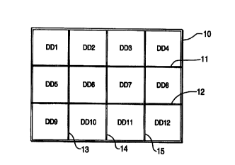
One conventional solution is to create a larger display by placing several
smaller
displays side by side. For example, twelve television sets or other CRT
displays DD1
through DD12 could be stacked up three high by four wide to create a large
screen display 10
2 s in which one-twelfth of the image is displayed on each television set DD 1
- DD 12, as
illustrated in FIGURE 1. However, because the CRT in each television set both
does not
display an image all the way to the edges of its faceplate, and because the
glass envelope of
the faceplate is not exactly rectangular, there will necessarily be horizontal
and vertical spaces
11, 12, 13, 14, 15 between the edges of the respective CRTs where no image is
present.
3 o These spaces are often referred to as "seams" or "gaps." While designers
of large displays
gU~s'fiTtJTE SHEET (RULE 2~
CA 02308476 2000-OS-03
WO 99/29117 PCT/US98/25552
have tried to minimize the inactive edge areas of display modules comprising
such display,
and thereby minimize these seams or gaps, they have not been able to eliminate
them, and so
visible and annoying gaps remain in the images displayed by such devices.
Even with rear-projection systems, the mullions of their respective diffuser
panels
leave a visible image-less seam. Front-projection systems have eliminated the
mullion
problem, but have great difficulty in projecting a true combined image in the
seam areas
which are usually sought to be minimized by involved and time-consuming
complex set up
and alignment procedures. In any of the foregoing arrangements, differences in
resolution,
geometry, brightness, intensity, and color between the portions of the
combined image, or
io sub-images, produced by the various display units making up a larger
display can produce
noticeable variations in the displayed image. Such effects are well known and
easily seen, for
example, in the jumbo television displays often used at sporting arenas,
concerts and outdoor
events.
In addition to the desire for large image size, there is also a need for high
image
i5 resolution along with large size. This need is evident, for example,
regarding high-definition
television (HDTV) systems and industrial and military displays. For high-
definition displays
of maps and charts, or of surveillance images, displays having resolutions of
I00 dots per
inch over a 30 x 40 inch display are desired. Such images include I2 mega-
pixels of
displayed information. Unfortunately, displays having such capabilities do not
exist with
2 o conventional technologies. It is further desirable that such large display
devices be easily
transported and set up, and that they be available at a reasonable cost.
Accordingly, there is a need for a display system that is capable of providing
high
resolution and a virtually seamless image even over a relatively large display
area.
To this end, the present invention comprises at least two image generators
generating
2s adjacent portions of an image on a screen, wherein the adjacent portions of
the image overlap;
and an image processor providing image data to the image generators including
pixel data
representative of particular pixels in the overlap that are adjusted so that
the respective pixels
generated therein by the two image generators combine to form the particular
pixels.
According to another aspect of the present invention, a method of forming a
3 0 substantially seamless pixelated image comprises:
SUBSTITUTE SHEET (RUSE ?.~
CA 02308476 2000-OS-03
WO 99129117 PCTNS98125552
forming two contiguous pixelated sub-images having a region of overlap at
their
common edge;
determining the value of particular pixels in the region of overlap;
determining a correction function for changing the determined value of the
particular
s pixels in the overlap region to a given value; and
applying the correction function to respective pixel values of each of the
pixelated
sub-images for each of the particular pixels in the overlap region.
BRIEF DESCRIPTION OF THE DRAWll~IG
io The detailed description of the preferred embodiments of the present
invention will be
more easily and better understood when read in conjunction with the FIGURES of
the
Drawing which include:
FIGURE 1 is a diagram of a prior art modular display device;
FIGURE 2 is a schematic block diagram of an exemplary embodiment of a display
i5 system according to the present invention;
FIGURE 3 is a representative diagram of a portion of an exemplary image
generator
usable with the embodiment of FIGURE 2;
FIGURE 4 is an exploded view of an exemplary physical embodiment of a portion
of
an image generator usable with the embodiment of FIGURE 2;
2 o FIGURE 5 is a diagrammatic representation illustrating the relationship
between the
size and number of sub-images and a dimension of a display system;
FIGURES 6 and 7 are diagrams showing side and front views of another
alternative
exemplary physical embodiment of a portion of an image generator usable with
the
embodiment of FIGURE 2;
2s FIGURES 8(a) and 8(b) are diagrams showing front views of another
alternative
exemplary physical embodiment of an image generator usable with the embodiment
of
FIGURE 2;
FIGURE 9 is a cross-sectional view of the image generator of FIGURE 8(a};
FIGURE 10 is a cross-sectional view of a portion of the image generator of
FIGURE
3 0 8(b);
suesmurs sH~T cau~ aa~
CA 02308476 2000-OS-03
WO 99/29117 PGTNS98/~5552
FIGURES 11 (a), I 1 (b), 11 (c) and 11 (d) are detail diagrams relating to an
image -
generator element of a sort useful in the image generator of FIGURE 10;
FIGURES I2 and 13 are cross-sectional diagrams of an alternative embodiment of
an
image generator of the sort shown in FIGURE 3;
s FIGURES 14(a) and 14(b) are diagrams of an image and sub-images in relation
to the
image generators of FIGURES 4 and 12;
FIGURES 15 and 16 are diagrammatic representations of an embodiment of a
modular display system according to the present invention;
FIGURE 17 is a cross-sectional diagram of a high-brightness image generator
relating
i o to the embodiment of FIGURES 15 and 16;
FIGURE 18 is a schematic block flow diagram relating to the embodiment of
FIGURES 15 and 16;
FIGURE 19 is a schematic block diagram relating to the flow diagram of FIGURE
18;
and
is FIGURE 20 is a schematic block flow diagram relating to the embodiment of
FIGURES 15 and 16.
DESCRIPTION OF THE PREFERRED EMBODIMENTS
2 o In the display system of FIGURE 2, an exemplary display system 100
includes a
display screen 102 on which an image is displayed and a plurality of image
generating
devices or modules 110, 120, 130, 140. In this example, a 2 x 2 array of four
image
generators or modules 110, 120, 130, 140 (which are not fully visible in
FIGURE 2), which
may be only a portion of a larger display system, generate the image display.
Screen 102 may
2 s be a faceplate on which is arrayed a pattern of phosphor elements, such as
stripes or "dots,"
that emit light when illuminated by an electron beam, as on the faceplate of a
color display
CRT. Each of image generators 1 I0, 120 ... generates an electron beam that is
scanned across
the portion of screen 102 that is proximate to that image generator and which
electron beam is
modulated in intensity in accordance with the image data to modulate the
brightness of the
3 0 light produced by each phosphor element, thereby to produce a portion, or
sub-image, of the
4
suesmuTE sH~r tRU~ z~
CA 02308476 2000-OS-03
wo ~n9i ~ ~ rcr~rs9snsss2
total image displayed.
Alternatively, screen 102 may be an optical (light) distributor that transmits
and
distributes light when it is illuminated by a light beam, as on the screen of
a rear-screen color
projection display. An optical distributor receives an incoming beam of light
coming from a
given direction and spreads the outgoing beam of light angularly over a
desired region, such
as a solid angle. For example, a diffuser is a distributor that operates by
scattering incoming
light. In this case, each of image generators 110, 120 ... generates a light
beam that
illuminates the portion of screen 102 that is proximate to that image
generator and the light
beam is modulated in intensity in accordance with the image data to modulate
the brightness
to of the light transmitted by distributor screen 102, thereby to produce a
portion, or sub-image,
of the total image displayed. As is described below, the image portion
displayed on screen
102 by each display module 110, 120 ... overlaps along each of its edges the
image portion
displayed by the display modules adjacent thereto, whether such display
modules are
physically mounted in a display module structure or are mounted in separate
display module
is structures that are abutted one to the other, thereby avoiding any inter-
module gap. Thus
there are areas of overlap and no seams or gaps between the image portions or
sub-images
produced by the various display modules. Display modules 110, 120,... may
employ active
matrix liquid crystal display (AMLCD) devices of the sort that are widely
employed in laptop
computers. Suitable AMLCD panels include type LT-170E101 commercially
available from
2o Samsung located in Seoul, Korea.
The overlapping of adjacent sub-images in a seamless fashion requires the
ability to
correct at least the intensity of the pixels of each sub-image in its overlap
regions. This
requirement is addressed by image processing that adjusts or predistorts each
sub-image,
preferably on a pixel-by-pixel basis, and controls the intensity of the pixels
that comprise
2 s such sub-image. It is also provided that the image processing adjusts or
predistorts each sub-
image in regions outside of their respective overlap regions to compensate for
differences
between and among the various image generators.
Associated with each image generator 110, I20 ... is a respective image
processor
IP1, IP2, IP3, IP4 that respectively processes image data received from an
image server 106
3 o and generates image data on a pixel-by-pixel basis for each pixel
reproduced by its associated
5
3V8ST1TUTE 8HE>ET (RULE 2~
CA 02308476 2000-OS-03
WO 99/29117 PCT/US98/25552
image generator I 10, 120, .., respectively. Image server 106, which may be a
commercially
available Pentium MMX processor, provides image data received from an image
source (not
shown, such as a static image memory or a network, or a source of plural
images sequenced
in time, as in a video or motion picture, or in space, as in an image mosaic,
and in any of a
s number of image data formats, such as compressed image data, graphic
language commands,
bit maps and the like) via data bus I05 for all the portions comprising the
image displayed on
screen 102 that it sends via a data bus 104 to each of the image processors
IPI, IP2, IP3, IP4.
Image processor IP 1 processes the image data for the portion of the image
produced by
image generator 110, such as by reformatting, decompressing, rendering,
decoding, and
io predistorting, and sends that modified image data to image generator I 10
on a pixel-by-pixel
basis. Images, and sub-images, formed on a pixel-by-pixel basis or resolvable
into pixels are
generally referred to herein as pixelated images. Image processors IPI - IP4
may be 350
MHZ Pentium MMX processor desktop-type computers (PCs) in conjunction with
respective mufti-media processors to perform the real-time digital corrections
of the image
i5 data. Each Pentium MMX processor PC, may include a 128-Megabyte (MB) SDRAM
memory, a 512-Kilobyte (KB) pipelined burst SRAM cache memory and a hard drive
to
perform the set-up, calibration, image acquisition and control of the mufti-
media processor.
Image server I06 may be a like computer. Such PCs are widely available from
many
manufacturers, such as IBM, Compaq, Hewlett Packard, Dell and Gateway, among
many
2 0 others.
The Matrox Genesis mufti-media processor commercially available from Matrox
Electronic Systems Ltd. of Quebec, Canada, is suitable for use in image
processors IPI - IP4
of the display system described herein. The Matrox Genesis processor is
capable of operating
at 100 billion operations per second (BOPS) and so can directly provide image
data for
2 s displays having up to 1600 x 1200 24-bit pixels in response to input image
data provided by
either digital or analog cameras, or other sources. Processing is performed by
a Texas
Instrument C80 processor that is capable of accelerating the full range of
operations
employed in image processing, such as point-, neighborhood- geometric- and
pattern-
matching operations. The Matrox Genesis mufti-media processor further includes
a
s o Neighborhood Operations Accelerator ASIC (NOA2) that further accelerates
image
6
SU9ST1TUTE SHEET (RULE ?6j
CA 02308476 2000-OS-03
wo ~r~9»7 pcrius9snsssa
processing operations, such as convolutions, morphology, normalized gray-scale
correlations,
and that also includes a JPEG coder/decoder (codec). Even with a processor
operating at 2
BOPS, for example, the multi-media processor can perform about 2000 operations
per pixel
per second; which would allow the image data to be updated about three to ten
times per
s second under a typical condition where about four-hundred digital operations
per pixel are
required for digital image correction in a display system having a 4 x 4 array
of image
generators.
Shown in phantom in FIGURE 2 is a sensor 108 that is temporarily put into
place to
sense the image displayed on screen 102 for purposes of set up and/or
calibration. Sensor 108
to may be a CCD television camera or other similar sensor. For calibration or
set up, image
server 106 causes a predetermined image, such as a checkerboard, cross-hatch
or other test
pattern, to be displayed on screen 102. The test pattern image is observed via
sensor 108 for
uniformity of brightness, alignment of edges and other image characteristics.
At certain times
sensor 108 senses the entire image area of screen 102, at other times senses
ones of the sub-
images thereon, and at yet other times senses the overlap regions of
contiguous sub-images,
for generating appropriate correction functions for uniformity of brightness,
pixel registration,
focus distortion and other characteristics of the image and particular pixels
or neighborhoods
of pixels thereof. Image server 106 and image processors IP1 -IP4 adjust the
relative
brightness of the respective sub-image generators 110, 120, ... for a uniform
brightness across
2 o the display on screen 102, adjust the alignment of edges and lines by
shifting sub-images
horizontally or vertically, and may also adjust other display characteristics
such as
colorimetry, in an iterative process employing updated data from sensor 108. A
Sony model
SSC-C370 CCD television camera available commercially from Edmund Scientific,
located
in Barrington, New Jersey, is suitable for sensor 108.
2 s Alternatively, server 106 may be eliminated and the functions performed
thereby as
described above may be performed by image processors IP1,... IP4 being
directly coupled to
the image source, such as an Ethernet or other network, as illustrated by the
data buses 105'
and 109' shown in phantom in FIGURE 2, as may be desirable where a modular
display
system 100 is desired. In this embodiment, each display module (including an
image
3o processor IP1,... IP4 and an image generator 110, 120...) determines the
portion of the image
SUBSTITUTE SHEET (RULE 2is)
CA 02308476 2000-OS-03
WO 99/Z9117 PCTNS98/25552
data that it will accept and respond to. Image data received via Ethernet or
other network
105' is applied via data bus 104 to image processors IP1,... IP4, each of
which selects and
accepts those portions of such image data that it can utilize to generate its
respective portion
of the sub-images, for example, by reading and acting upon the header data and
control data
s included in the information packets containing image data sent via network
104, 105'.
Similarly, image data from display screen 102 sensed by sensor 108 is applied
directly via
data buses 109, 109' and 104 to image processors IP1,... IP4, , each of which
selects and
accepts those portions of such sensed image data that it can utilize to
correct its respective
portion of the sub-images.
Data buses 104, 105, 105', 109, 109' may be, for example, Ethernet or LAN or
similar
commercially available networks capable of data communication at a data rate
of about 100
Megabits per second (MBPS). If the image stored in image server 106 or
received via
network 105' is a bit-mapped image having 16 Megapixels of 24 bits each, the
image will
load to image processors IP1 - IP4 in about four seconds. This image transfer
rate can be
s5 increased, if necessary, by increasing the data transmission rate of data
buses 104, 105, 105'
such as to 200 MBPS, or by compressing the image data prior to transmission
thereof to
image processors IP1 - IP4 which then de-compress the image data after
receipt, in known
manner.
Thus, the display system of the present invention forms overlapping sub-images
with
2o redundant pixels and then performs real-time digital signal processing to
preserve
substantially full resolution in the overlap regions and may also compensate
for image
generator variations, physical tolerances, optical imperfections, distortions,
setup errors, and
drift, for pixels in the overlap region as well as for pixels outside of the
overlap region of the
sub-images. Overlapping images are reformatted in reai-time by a PC-based
system that
2s compensates for the image overlaps, individual image distortions, pixel
position errors and
sub-image-to-sub-image matching so that there are neither visible seams nor
apparent loss of
resolution between the sub-images that together comprise the displayed image.
To this end, sensor 108 is directed particularly to the regions of overlap
between
adjacent sub-images. For example, without correction, the overlap regions
would be brighter
3 o than the surrounding sub-images because more than one image generator 110,
120 is
8
Su88T1TUTE SHEET (RULE 2~
CA 02308476 2000-OS-03
WO 99/29117 PCT/US98I25552
generating those pixels. In response to data from sensor 108, image server 106
controls
image processors IP1, IP2, ... to reduce the brightness of their respective
edge-region pixels
so that the combined image is of the correct brightness level. In other words,
to compensate
for such increased brightness, each pixel sent to one of image generators 110,
120, ... is
s comprised of a weighted linear combination of the local neighborhood of
pixels in the source
image, for example, pixels in a 2 x 2 pixel neighborhood. For pixels in the
regions of overlap
of the sub-images, the values of the pixels in each sub-image contributing
thereto is weighted
so that the combined total value for each pixel corresponds to the value of
that pixel in the
source image, for example, as by proportional weighting. Thus, the image
intensity is not
to simply "feathered" in the overlap regions, but can be corrected to any
desired degree, both in
the overlap regions of the sub-images as well as in the remainder thereof,
limited by the
processing capabilities of the processors 110, 120 employed.
In addition to the pixel intensity being digitally adjusted to blend the
images in the
overlap region and to account for the differences in the intensity transfer
characteristic of the
is image generators, the pixels in each sub-image can also be predistorted or
"warped" to
compensate for geometrical and other distortions in the optics or scanning
structures of image
generators 110,120. Further, chromatic aberrations can be con-ected by making
the
geometrical compensation color-dependent; pin-cushion and barrel distortions
can also be
corrected by image transformation in image processors 110, 120,....
2 o For example, if two image generators 110, 120 are contributing to a given
pixel, then
the brightness of each image generator is reduced proportionately, such as to
produce about
one half of the total brightness. Thus, in an eight-bit pixel value display,
if a pixel in the two-
sub-image-overlap region has a value of 162 (out of 256) in the source image,
the sum of the
two contributing sub-image pixel values will be 162. Thus, each may have a
value of 81, or,
2s alternatively, one could have a value of 102 and the other a value of 60,
or any other
combination of values summing to 162. Similarly, if four image generators 110,
120 are
contributing to a given pixel, as is the case in corners of sub-images where
four sub-images
overlap, then the brightness of each image generator is reduced
proportionately, such as to
produce about one fourth of the total brightness. Thus, if a pixel in the four-
sub-image-
3 0 overlap region has a value of 184 (out of 256) in the source image, the
sum of the four
SUBSTITUTE SHEET (RULE 2~
CA 02308476 2000-OS-03
wo ~n9m Pcr~s9snsssz
contributing sub-image pixel values will be 184. Thus, each may have a value
of 46, or,
alternatively, ones could have respective values of 36, 42, 50 and 56, or any
other
combination of values summing to 184. Thus, image processors IP1, IP2, ..
adjust the
brightness of each pixel in each overlap region so that the combined total
brightness from all
s image generators contributing to any particular pixel is the correct pixel
brightness for that
pixel in the displayed image, for example, by applying a proportionately
weighted correction
factor. In addition, image processors l:Pl, IP2, .. also adjust the brightness
of each pixel in
each sub-image so that the total brightness level produced by each of the
image generators is
uniform over the entire displayed image, in conjunction with adjusting the
values of sub-
1o image pixels contributing to any particular pixel in the displayed image,
whereby each pixel
has the correct source-image pixel brightness for that pixel in the displayed
image.
It is noted that the correction or adjustment of pixel values may be based
upon
characteristics of individual pixels or upon characteristics of pixels in a
neighborhood of
pixels, and that such characteristics may include pixel intensity or
brightness and/or pixel
15 position. As a result the fully digital processing and display panel drive
enable the corrected
image information to be accurately placed at the correct color pixel location
in a sub-image
with the correct intensity, and for each sub-image to be accurately placed at
the correct color
pixel location in the complete image with the correct intensity.
The aforementioned image data is structured by image processors IP1 - IP4 in
the
2 o manner appropriate to the particular input source image data format,
whether from image
server 106 or from a network 105, 105'. FIGURE 3 is an expanded diagram
showing two
adjacent exemplary image generators, such as image generators 110, 120 shown
in FIGURE
2. Image generators 1 IO and I20 are preferably active matrix liquid crystal
displays
(AMLCD) of the sort currently found in laptop portable computers on which a
plurality of
2 s image portions or sub-images are produced. Image generator 110 produces
image portions or
sub-images in display areas I I 1, 112, 113 that are slightly expanded or
enlarged by lenses
117, 1 I8, 119 (each of which may include a plurality of optical elements or
lenses) to produce
overlapping sub-images I I 1', I 12' 113' on screen 102. In like manner, image
generator I20
produces image portions or sub-images in display areas 121, 122, 123 that are
slightly
3 o expanded or enlarged by lenses 127, 128, 129 to produce overlapping sub-
images 121', 122'
suesnruTE sH~ tAU~ ~
CA 02308476 2000-OS-03
WO 99/29117 PCT/US98/ZS552
123' on screen I02. In FIGURE 3 the extremes of the light beams of each sub-
image are-
represented by beams 114, 115, 116, 124, 125, 126, and the curved arrows
associated
therewith. Note that even though adjacent display areas 111, 112, 113, 121,
122, 123 are
separated by gaps, i.e. they are not contiguous, the corresponding sub-images
1 I I', 112',
s 113', 121', 122', 123' on screen 102 overlap and have no seams or gaps. The
same is true for
image generators 110 and 120 which may be spaced apart, and so may have a
substantial edge
area or a gap where no image is produced, yet the adjacent sub-images 1 I3'
and 121'
produced respectively by adjacent sub-image display areas 113 and 121 also
have an overlap
region along their adjacent edges. Accordingly, the heretofore virtually
unsolvable problem
io of creating an image generator that generates images all the way out to its
edges is eliminated,
as are objectionable seams and gaps.
FIGURE 4 illustrates an expanded or exploded view of an exemplary physical
embodiment of the image generator 110 and its associated elements of FIGURE 3.
AMLCD
image generator 110 includes a transmissive liquid crystai panes 50 that is
logically
15 segmented to display a plurality of adjacent, non-contiguous sub-images
111, 112 thereon in
response to image data, i.e. not all the available display area is utilized
for producing sub-
images. In particular, the specific pixels of image generator 110 that display
each sub-image
111, 112 are selected for proper registration of the adjacent sub-images 111',
112' on screen
102 with predeternuned overlap (illustrated as regions on screen 102 enclosed
by dashed
20 lines), and the other areas of image generator 110 are blanked
electronically. AMLCD panel
50 is back-lit by light produced by lamp light source and collimator 54, which
light is further
collimated by Fresnel collimator array 52. As sub-image I I 1, for example, is
generated, light
beam 114 therefrom passes through lens 117 and illuminates sub-image portion
111' on
screen 102. Lenses 117, 118 ... are fabricated in a matrix layer and have
slightly greater than
2s unity magnification. It is noted that high screen pixel densities are
achieved by this
arrangement. For example, if 75% of the available linear dimension or 75% x
75% = 56% of
the available area of a 13.3 inch diagonal 1600 x 12()a pixel AMLCD panel 110
is utilized to
produce a 14 inch diagonal sub-image on screen 102, the resulting sub-image
has a resolution
of about a 1200 x 900 pixel, or about 1.6 mega-pixels per square foot.
3 0 FIGURE 5 shows three representations of exemplary modular display systems
of the
m
8U6STtT1;ITE SHEET (RULE 2~
CA 02308476 2000-OS-03
wo ~n9~ i ~ rc~r~s9ensssi
sort described in relation to FIGURES 2 - 4 above to illustrate the
relationship between the
size and number of the sub-images employed and the depth dimcnsion "D" of the
modular
display system, for a particular size "I" of the displayed image. In the upper
representation,
one relatively large image 150 is generated to produce the displayed image and
the resulting
s display system depth is relatively large. In the middle representation, two
relatively smaller
sub-images 152A, 152B are generated to together produce the displayed image
and the
resulting depth D is substantially smaller than in the one-image example. In
the lower
representation, four relatively smaller yet sub-images 154A, 154B, 154C, 154D
are generated
to produce the displayed image and the resulting depth D is relatively smaller
yet. One
to advantage of this arrangement is that the beams from adjacent image
generators impinge upon
the screen at almost the same angle of incidence which beneficially reduces
image variations
on a diffusive screen, particularly for viewers who are viewing from positions
off the central
axis of the display. As noted above, the adjacent sub-image generators need
not be
contiguous to develop a seamless displayed image. Because the lenses have
magnification of
is greater than unity and the displayed sub-images overlap, the reduction of
depth D that results
from each doubling of the number of sub-images is less than one half the
depth.
FIGURES 6 and 7 are respectively side and front views of an alternative
embodiment
of a portion of a display system according to the present invention that
employs a plurality of
large-area optical projectors 210, 230... as the image generators 110, 120...
of FIGURE 2.
2o Projector 210, which may have the light projected through projection lens
220 modulated by
a liquid crystal panel, projects a sub-image onto optical distributor screen
202 via a three-
stage folded-minor optics arrangement including first mirror 212, intermediate
mirror 214
and final mirror 216. Mirrors 212, 214, 216 are preferably flat, but may be
convex to provide
additional magnification. The center line of the sub-image projected by
projector 210 is
2 s represented by light ray 224 and the upper and lower edges thereof are
represented by light
rays 222 and 226, respectively. Similarly, projector 230, which may also have
the light
projected through projection lens 240 modulated by a liquid crystal panel,
projects a sub-
image onto screen 202 via a like folded-mirror optics an:angement including
first minor 232,
intermediate mirror 234 and final mirror 236. Mirrors 232, 234, 236 are
preferably flat, but
3 o may be convex to provide additional magnification. The center line of the
sub-image
12
sues sH~r ~RU~ zap
CA 02308476 2000-OS-03
wo ~n9»~ pc~rivs98nsss2
projected by projector 230 is represented by light ray 244 and the upper and
lower edges
thereof are represented by light rays 242 and 246, respectively. Adjacent sub-
images
projected by projectors 210, 230 overlap in a region 248 along their
respective edges, as
indicated by the intersection of light rays 226 and 242 before they impinge
upon screen 202.
s In FIGURE 7, a front view of the portion of the display system of FIGURE 6,
four
optical projectors 210, 230, 280, 290 are arrayed to project adjacent sub-
images that overlap
in horizontal and vertical regions 248 along their respective peripheries as
is illustrated by the
darkened vertical and horizontal bands forming an array of rectangles.
Intersections of the
overlap regions 248 are designated 252, 256, 260, 264, 268. An advantage of
this
so arrangement is that sensors to sense the pixels in the overlap regions 248
of the displayed
image can be positioned behind screen 202 rather than in front of the screen
(as is the case
illustrated for sensor 108 in FIGURE 2), thereby being better able to remain
in position and
operating while the display system is operating to display images rather than
only during set
up and calibration operations. To this end, a plurality of sensors such as CCD
cameras 250,
Zs 254, 258, 262, 266 are positioned to sense pixels in the intersections 252,
256, 260, 264, 268,
respectively, of overlap regions 248 for processing by image server 106 and
image processors
IP 1 -IP4 as described above. This produces pixels in the overlap regions by
combining pixels
produced by adjacent image generators 210, 230, 280, 290 which are generated
in relation to
each other and the true pixel, so that the resulting combined pixels are those
of the image
2 o being displayed. The number of sensors required for sensing the overlap
intersection regions
in an array of M x N sub-image generators is given by (M+1)(N+1) = MN + M + N
+ 1 for
the arrangement shown in FIGURE 7. In addition, one sensor is employed for
each optical
projector for sensing and mapping the image intensity profile of each sub-
image display
which is digitally processed by image server 106 and image processors IP1 -
IP4 to make
2 s uniform the intensity pattern of the overall image, such as by digital
apodization of the
luminance data. It is noted that the correction of pixel values may be based
upon
characteristics of individual pixels or upon characteristics of pixels in a
neighborhood of
pixels, and that such characteristics may include pixel intensity or
brightness and/or pixel
position.
3 o In a typical projection display arrangement 200 of the sort shown in
FIGURES 6 and
13
suesrtruTE sH~r ~u~ ~
CA 02308476 2000-OS-03
WO 99/29117 PCT/US98/25552
7 in which each projector 210, 230 projects a sub-image that is 18 inches high
by 24.5 inches
wide and that overlaps the adjacent sub-image by two inches, a 56.5 inch
optical length via
the folded-mirror optics is achieved in a physical depth of about 36 inches.
Suitable optical
projectors include type X-200 commercially available from Mitsubishi located
in Cyoress,
s California, and suitable CCD cameras include Panasonic type GP-US502
commercially
available from Edmund Scientific located in Barrington, New Jersey.
FIGURES 8 - 10 show a display system in which plural overlapping sub-images
310,
320, 330, 340, 350 ..., 360 shown in FIGURE 8(a) are produced on the faceplate
302 of a
large unitary glass-front evacuated housing 300. A plurality of sub-image
generators of sub-
1 o images 310 - 360 are located within housing 300 and may include a
plurality of cathodo-
luminescent sources such as thermionic cathodes, semiconductor field emitters
or other
electron sources that project a large number of synchronously-scanned,
modulated electron
beams onto color (red, green, blue) phosphor elements, such as dots or
stripes, on faceplate
302. Areas of overlap around the respective peripheries of sub-images 310,
320, 330, 340,
1 s 350 ..., illustrated, for example, by the regions 312, 322, 332, 342
between dashed lines,
include pixels that are combinations of the respective pixels generated by
adjacent sub-image
generators that have been digitally processed to together produce the true
image pixels, as
described above. Exemplary sub-image 360 is enlarged in FIGURE 8(b) to show
the relative
locations of exemplary ultra-violet-light producing phosphor elements,
illustrated as small
2 o black squares such as 362, 364, 366. Ultra-violet dots 362, 364, 366 ...
are employed as
sensors for monitoring pixels in the areas of overlap of adjacent sub-images
for setting and
adjusting the registration and focus of the respective sub-images, and for
synchronizing the
scanning of the respective sub-image generators. Once the registration and
scanning is
adjusted, ultra-violet dots 362, 364, 366 ... are employed as sensors for
monitoring pixels in
2s the areas of overlap of adjacent sub-images for setting and adjusting the
brightness or pixel
intensity of each sub-image and therefore the uniformity of the brightness and
pixel intensity
over the complete displayed image. Exemplary area 370 on faceplate 302 is
enlarged to show
an exemplary pattern of color phosphor stripes thereon, in particular, red
stripe 372, green
stripe 374 and blue stripe 376, each of which is separated from the adjacent
stripes by a black
3 o stripe (i.e. the "black matrix" pattern) for improving contrast.
14
sues~r>TU~ sH~r ~au~ asp
CA 02308476 2000-OS-03
WO 99/Z9117 PCTNS981Z5552
FIGURE 9 shows a cross-section of vacuum enclosure housing 300 of FIGURE $(a)
including a large area phosphor-striped glass CRT faceplate 302 attached by a
frit vacuum
seal 303 along its periphery to a structural backplane 304, whereby a 45-inch
diagonal display
having a resolution of 13 megapixels per square foot and a thickncss of only
about ten inches
s is provided. Smaller displays and lower pixel resolution displays may also
be provided, and
supports may be required for the inner surface of the glass screen for larger
screen sizes.
Electrical leads 305 are brought out of the vacuum enclosure 300 through the
frit seal 303 in
conventional manner. Housing 300 is evacuated by creating a vacuum on
evacuation exhaust
port 306 which passes through structural backplane 304. After housing 300 is
evacuated,
to exhaust port 306 is sealed and any remaining gas molecules are absorbed by
getter 308 in
known manner. The plurality of image generators are mounted on image generator
assembly
400 within housing 300 as is described below.
In FIGURE 10, image generator assembly 400 includes a ceramic support rail 402
on
which are mounted a plurality of electron sources, such as field emitter
elements 404, 406
i5 formed on respective semiconductor chips. Each field emitter element 404,
406 is flanked to
the left and right by respective electrostatic horizontal focus/deflection
plates 410, 412, 414
which respectively deflect the electron beams 424, 426 produced by the
respective field
emitter elements 404, 406 horizontally (e.g., left to right in FIGURE 10).
Electrostatic
vertical focus/deflection plates, such as plate 416, are oriented orthogonally
to horizontal
2o focus/deflection plates 410, 412, 414 and also flank field emitter elements
404, 406 (e.g.,
plate 416 is below the plane of the paper in FIGURE 10 and another vertical
plate (not
shown) is above such plane) and deflect the electron beams produced by the
respective field
emitter elements 404, 406 vertically, i.e, above and below the plane of the
paper. In addition
to the deflection signals applied to respective focus/deflection plates 410,
412, 414, 416..., a
2s respective focus signal is applied thereto to adjust the focus of the beams
of electrons 424,
424 generated by each field emitter element 404, 406, respectively, so that
the electron beams
each converge at a respective spot on the inner surface of screen 302, as is
illustrated by
converged electron beams 424 and 426.
All of the electron beams have areas of overlap scan with the adjacent scanned
3 o electron beams around the peripheries of the respective areas covered by
each respective
sues~rti ruTE sH~r tRU~ zap
CA 02308476 2000-OS-03
WO 99I291i7 PCTNS98lZ555Z
scanned electron beam, and preferably are scanned in synchronism. It is noted
that the
combined actions of field emitter element 404, horizontal and vertical
focus/deflection plates
410, 412, 416 function as a lens that enlarges the sub-image generated by
field emitter
element 404 to produce on screen 302 an enlarged sub-image that overlaps the
sub-image
produced thereon by the adjacent, but not contiguous, field emitter element
406. The same is
true for each of the field emitter elements and their associated horizontal
and vertical
deflection plates, as well as for the sub-images 310, 320... of display 300.
Phosphor pattern 370 is on the inner surface of glass screen 302 and comprises
repetitive sequences of color phosphor stripes thereon, for example, red
stripe 372, green
to stripe 374 and blue stripe 376, each of which is separated from the
adjacent stripes by a black
stripe (i.e. the "black matrix" pattern) for improving contrast. As electron
beams 424, 426 are
scanned across the color phosphor stripes 372, 374, 376 of phosphor pattern
370 they are
modulated with luminance and chrominance information representative of the
individual
pixels comprising the image displayed on screen 302 to produce such image
thereon.
Electron beams 424, 426 preferably raster-scan in synchronism between the
edges of the
respective sub-images they produce, as illustrated in FIGURE 10 by solid lines
and dashed
lines, respectively, representing the beginning and end, respectively, of each
beam's scan
represented by the curved arrow therebetween.
Ultra-violet-emitting phosphor dots such as dots 362, 368 are located on the
black
2o stripes of phosphor pattern 370 for being illuminated by and for sensing
and monitoring
respective ones of the electron beams 424, 426 in the regions of screen 302 in
which they
(and the respective sub-images they produce) overlap. For a screen 302 that
displays a 300 x
124 pixel sub-image, less than 100 UV phosphor dots 362, 368 distributed over
the area of
screen 302 are required to sufficiently measure the horizontal and vertical
landing position
2 s data of the various electron beams. Preferably, UV phosphor dots 362, 368
are located on
respective black stripes, for example, ones that separate a red phosphor
stripe 372 from a
green phosphor stripe 374. When illuminated by the electron beams 424, 426, UV
phosphor
dots 362, 368 emit UV light, such as UV light beams 428, 429 emitted by UV
phosphor dots
368, 362, respectively, in response to electron beams 424, 426, which UV light
beams 428,
30 429 in turn illuminate UV sensor chip 384 and 386, respectively. In like
manner at the other
16
sues~mvr>E sH~t ~u~ a.~
CA 02308476 2000-OS-03
WO 99129117 PCT/US98Ix555Z
end of the scan, exemplary electron beam 424 illuminates UV phosphor dot 362
which emits
UV light 429 that impinges on UV sensor chip 386.
Variations in the landing position (registration), focus and intensity of the
electron
beams 424, 426 arise, for example, from chip-to-chip differences in the field
emitter
s elements, physical placement tolerances for the field emitter elements and
the horizontal and
vertical deflection plates 410, 412, 414, 416.... Detection of electron beam
424 impinging on
UV phosphor dots 368 and 362 enables UV sensor chips 384, 386, res~ctively, to
signal the
times thereof so the appropriate processor, such as image processors IP1 -
IP4, can
synchronize the scanning and timing of all the electron beams and can further
control the
io width and length of the scanning of each electron beam, as well as its
registration, focus, a.nd
intensity, thereby creating each pixel of the image displayed, including those
pixels produced
by combining the sub-image pixels produced by plural image generators in the
overlap areas,
with its correct registration and intensity.
It is preferred that UV sensor chips 384, 386 and/or field emitter chips 404,
406
i5 include or be associated with processor and memory devices that perform the
aforementioned
processing and corrections as well as the beam alignments described below to
adjust or
correct to a predetermined standard the characteristics of the sub-images
produced by each
field emitter element during operation of the image generators. UV sensor
chips 384, 386
and/or field emitter chips 404, 406 may be fabricated to include processors
and addressable
2o memory on one or more semiconductor chips. The connections calculated by
the processor
from the measured beam landing and timing information are stored in the
addressable
memory, such as in a look-up table, from which they are later retrieved to
control the
generation of the respective sub-images of the displayed image. Exemplary
correction
information stored in such addressable memory includes, for each field emitter
element, the
2s voltages to be applied for proper (i.e. predetermined standard) intensity
characteristics, the
columns of the field emitter arrays to be activated for proper horizontal beam
positioning, the
advancement or retardation of the column enabling pulse for proper vertical
beam positioning
within a row, and the voltages to be applied to the vertical and horizontal
deflection plates for
proper scanning synchronism and proper beam focus.
3 o One exemplary way in which the timing and landing accuracy (registration)
of the
i7
SUHgTrTUTE 8HEE'f' (RULE 2~j
CA 02308476 2000-OS-03
WO 99/29117 PCTNS98/2555Z
respective electron beams is controlled is illustrated by Figures 1 I (a), 11
(b), 11 (c) and 1-1 (d).
A portion 570 of the color phosphor stripe pattern includes red stripe 572,
green stripe 574
and blue stripe 576 with black non-phosphor stripes 578 therebetween. An
exemplary UV-
phosphor dot 568 of generally rectangular shape is on one of the black stripes
578. For a 10-
mil by 10-mil (0.25 x 0.25 mm) square pixel, for example, typical for
contemporary high-
performance CRT monitors, each color phosphor stripe and each black matrix
stripe is 1.67
mils wide and so a beam width of about 2.5 t 0.5 mil is required for each
electron beam. An
exemplary field emitter element in the form of semiconductor field emitter
chip 504 includes
an array 506 of addressable field emitting sites arranged in rows and columns,
for example, in
so a 20 x 20 array with about 5 im center-to-center spacing of the individual
field emitter sites.
With a magnification of about two times in the deflection system, an image of
the addressed
columns having about a 10 im spacing is produced across the 1.67 mil (42 im)
stripes. For
this embodiment, the columns of field emitter chip 508 are addressed to select
the column
emitter sites that are to emit and all the rows thereof are simultaneously
enabled (i.e.
addressed) by a timing pulse for the time interval in which such emission is
to occur. In
FIGURE I 1(a), the field emitter sites in four adjacent columns 508 are
addressed and thus
emit respective electron beam lines that illuminate phosphor pattern 570 along
four lines 518
which, if they impinge on UV phosphor dot 568 cause it to emit UV light. The
magnitude of
the emitted UV light intensity is proportional to the intensity of the
electron beam
2 o illuminating phosphor dot 468, i.e. of the intensity of the electron beam
and the degree to
which it illuminates or misses phosphor dot 468. Thus, in the example of
FIGURE 11(a}, the
four lines 518 fall squarely on UV phosphor dot 568 and so the UV light
produced is high.
Horizontal correction or adjustment of the electron beam landing (e.g., across
the
stripe direction} is controlled by selecting the columns of field emitter chip
504 that are
2s caused to emit electrons. Thus in moving from the condition of FIGURE 11(a)
to that of
FIGURE 11 (b), in which the four lines 5 I 8 are translated horizontally to
the right as shown
by four lines 518', that translation is effected by an address that unselects
the four columns
508 of field emitter sites first addressed and instead addresses the four
columns 510 to the left
thereof. The columns selected can be varied in resolution of one column or
more, as is
3 o appropriate to the desired horizontal movement of the landing point of the
electron beam.
I8
suesmuTE sH»r ~u» z~
CA 02308476 2000-OS-03
WO 99/29117 PCT/US98/25552
Because the illumination of the UV phosphor dot 568 produces UV light that is
proportional
to the intensity of illumination, the spot size, and therefore the focus of
the electron beams
may be measured and adjusted by the respective image processors IP1 -1P4 so
that the spot
size is both reduced to substantially correspond to one pixel, or the width of
the color
phosphor stripes 572, 574, 576.
Vertical correction or adjustment of the electron beam landing (e.g., along
the stripe
direction) is controlled by addressing field emitter chip 504 by changing the
timing of the
timing pulse signals that cause field emitter chip 504 to emit. In FIGURES 11
(c) and 11 (d)
the horizontal lines 520 indicate time in cycles of the system clock signal,
where the time "n"
to is the nominal time at which the rows of field emitter chip 504 would
nonvnally be enabled to
emit. The notation "n+x" indicates timing that is "x" clock cycles later than
time "n" and "n-
x" indicates timing that is "x" clock cycles prior thereto. Thus in moving
from the condition
of FIGURE 11(a) to that of FIGURE 11(c), in which the four emission lines 518
are
translated vertically upward as shown by four lines 518', that translation is
effected by
is changing the starting time of the row timing pulse from the time "n+1" to
the earlier time "n-
1" The emission lines 518" in FIGURE 11(d) commence at time "n-3" and end at
time "n+1"
and so are further translated vertically upward from those of FIGURE 11 (c).
In each of these
examples, the row timing pulse is four clock cycles in duration, and the test
measurements are
preferably made with a checker-board test pattern displayed. For a 300 x 120
pixel sub-
2o image that is refreshed at a 75 Hz rate, the pixel frequency is
approximately 3 MHZ and so a
clock frequency of 18 MHZ or higher is sufficient to attain a localized
accuracy of less than
about 0.167 pixel, and an accuracy of about 0.25 pixel across the screen 302
display area.
In addition, because the electron beams 424, 426 from adjacent field emitter
elements
404, 406 in FIGURE 10 both illuminate the same UV phosphor dots during their
respective
2s scans, the UV sensor 386 can measure the registration and intensity of the
adjacent beams
which can then be adjusted or corrected by image server 106 and the respective
image
processors 1PI - IP4. Further, at each intersection of four sub-images in the
area of overlap at
their respective corners; the registration and intensity of the four electron
beams can be
measured and adjusted so that there is no visible remnant of a seam thereat.
In this regard,
3 o image server 106 and the respective image processors IP 1 - IP4 further
compute the
19
sues'r»uTS sH»r tAU~ asp
CA 02308476 2000-OS-03
wo ~n9m Pcrius9snsssz
proportionately reduced intensity required for each respective electron beam
so that the.
combination of the intensities of the respective electron beams in the overlap
areas is
substantially the same as that of each electron beam at any point in its sub-
image area. In
other words, the beam intensities are adjusted so that each pixel in the
displayed image,
whether generated as a pixel of a sub-image generated by one image generator
or as a
combined pixel in the overlap regions of plural sub-images, has the same
predetermined or
nominal intensity, thereby providing a uniform intensity level over the entire
area of the
displayed image.
In the alternative image generator module 1200 of FIGURE 12, an AMLCD panel
io image generator 1210 employs portions of its display as a plurality of
adjacent non-
contiguous sub-image generators 1211,..., 1213 that generate in conjunction
with lenses
1217,..., 1219 a plurality of overlapping sub-images 1211',..., 1213' on
display screen 1202.
Image generator module 1200 is similar to and operates in like manner to image
generators
I 10, 120 shown in FIGURE 3 and described above. Image generator module 1200
differs in
that it includes a thick optical structure 1230 through which light beams
1214,..., 1216 pass in
illuminating screen 1202 with their respective sub-images. Image generator
module 1200 has
several advantages and features, not the least of which is that it is a truly
modular image
generator that can be assembled side-by-side with other like modules 1200, as
shown in
FIGURE 13, in the field as well as in the factory or service center, to
display seamless
2o images. In addition, the arrangement of module 1200 provides places where
supports for the
screen may be placed without detracting from the image and facilitates the
sensing of
displayed image pixels from the rear.
To this end, optical structure 1230 has substantial thickness and has at each
of its
edges an optical surface 1232 that is substantially perpendicular to the plane
of screen 1202
2 s so that when placed side-by-side abutting a like module with an optical
gel or adhesive
material filling any voids therebetween, light beams from the adjacent modules
pass through
the optical interface formed by surface 1232 with insignificant reflection,
refraction or
distortion, thereby to preserve the overlapping sub-image arrangement with
respect to
abutting modules 1200.
3 o Conveniently, portions of the bottom surface of optical structure 1230
through which
sues~~rrv~ sH~r t>RU~ ae~
CA 02308476 2000-OS-03
WO 99/29117 PCT/US98nSS52
light beams 1214,... 1216 do not pass may be at least in part formed as flat
optical surfaces
1240 lying in one or more planes that are parallel to that of screen 1202.
Optical surfaces
1240 provide "windows" to screen 1202 through which the pixels displayed
thereon may be
monitored, such as by sensors 1250 which rnay be located behind modules 120(?
as shown or
s which may be embedded into modules 1200. Specifically, pixels in the overlap
areas of
adjacent sub-images (whether generated by adjacent image generator modules
1200 or by
adjacent sub-image generators 1211, 1212,... 1213 on a single module 1200) may
be sensed
from the back of the image generator module, thereby permitting set up and
calibration of a
multi-module display, as well as operational adjustments thereto, to be made
from the rear
to and without interfering with or interrupting the display of images to an
audience. Flat
surfaces 1240 along the edges of module 1200, may conveniently include tabs
and slots 1242
or other alignment and/or attachment features for facilitating the alignment
and/or attachment
of adjacent modules 1200 into a multi-module display. In addition, and perhaps
more
importantly, ones of surfaces 1240 not used as windows for sensing pixels
produced on
is screen 1202 may be employed for bearing locations for supporting members
positioned
between screen 1202 and panel 1210 as would be desirable for large display
screens, for
example, displays exceeding four feet along any edge.
To the end of sensing or monitoring the pixels in the regions of overlap of
various
sub-images, sensor 1250, which may be a CCD camera as previously described or
simply a
2 o CCD sensor chip, is located behind screen 1202 of image generator modules
1200 to view,
for example, selected regions of sub-image 1211', 1213' overlap. Sensor 1250
is coupled to
the image processor IP1 - IP4 that controls image generator module 1200 in the
manner as
previously described, to produce seamless images on screen 1202. Sensor 1250
may be built
into module 1200 or be a separate device. It is preferred that one or more
sensors 1250 be
2 s incorporated into each image generator module 1200 for sensing pixels in
various regions of
overlapping sub-images produced thereby, and in addition that one or more
sensors 1250 be
incorporated into each image generator module 1200 for sensing pixels in
various regions of
the sub-images produced thereby other than the regions of overlapping sub-
images. It is
further preferred that each module 1200 include electronic circuitry such as
non-volatile
3 o memory in which its set up and calibration parameters may be stored, and
from which such
21
suesmuTE sH~r tRU» zs~
CA 02308476 2000-OS-03
wo ~r~9m PcTius9snsssz
parameters may be readily accessed by the appropriate image processor IP1- IP4
for
facilitating the combining of modules into a multi-module display that
displays seamless
images. The parameters stored in such memory include, for example, correction
factors that
when applied to image data to be applied to the image generator 1200, render
its response to
be that of a predetermined standard despite the physical tolerances and
electrical tolerances of
the elements that comprise such module 1200. Further, the surfaces 1240
provide locations at
which screen 1202 may be supported, such as by a member attached between and
to surface
1240 and panel 1210. Because surface 1240 is not in the field of view of the
image
generators 1211, 1212,..., the addition of support such members does not
affect the image
i o quality.
Preferably, optical structure 1230 further includes on the rear surface
thereof arcuate
interface surfaces 1234 through which the light beams 1214,..., 1216 pass in
entering optical
structure 1230. Arcuate surfaces 1234 are preferably formed in a generally
spherical shape so
that light beams 1214,..., 1216 pass substantially perpendicular to the
surface 1234 to enter
~s optical structure 1230 with insignificant reflection, refraction or
distortion. Arcuate surfaces
1234 may be shaped so as to provide unity magnification or a greater
magnification.
It is apparent from FIGURE 12 as from FIGURE 4 that images in image generators
of
the sort shown therein invert an image from the image generator to the display
screen as a
result of the operation of their respective lenses. FIGURE 14(a) is an image
600 produced on
20 a display screen such as display screen 102 or 1202, which image is
comprised, for example,
of a 2 x 2 array of four sub-images 602, 604, 606, 608 as shown in FIGURE
14(b). Because
of the inversion produced by the lens; such as lens 117, 118, 119 or 1217,
1218, 1219, each
sub-image is itself inverted or "flipped" where it is generated. Each inverted
sub-image 602,
604, 606, 608 is inverted top-to-bottom and right-to-left by the lenses. For
example, the
2s bottom and right edges of upper left-hand sub-image 602 respectively become
the left half of
the top edge and the upper half of the left edge of image 600. The top edge of
sub-image 602
overlaps the bottom edge of sub-image 606 in a rectangular region located mid
way between
the top and bottom edges of image 600 and in the left half thereof. The fact
of sub-image
overlap is seen in that sub-images 602 and 606 both include the cross-bar of
the letter "A"
o and the cusp of the letter "B". Sub-image data inversion is performed in
image processors
22
sues~'tT~ sH»>= r tRUI~ ~
CA 02308476 2000-OS-03
WO 99/Z9117 PCTNS98/25552
IPl, IP2, ... such as by transformation filters that bitmap the pixel data of
each sub-image into
an addressable random access memory and then read out the pixel data in
reverse order, both
horizontally and vertically. Combination of pixel data for regions of overlap
may be
performed as pixel data for such regions are produced from the transformation
filters, such as
by combining sub-image data with appropriate weighting or correction factors.
Proportional
weighting may be employed, as may weighting based upon intensity
characteristics and/or
position of the respective pixels, whether for individual pixels or for pixels
in a neighborhood
of pixels.
FIGURE 15 shows a modular display system 700 according to the present
invention
io in a multiply-exploded representation to illustrate the formation of a
displayed image on
display screen 710. Display system 700 includes a display device or screen 710
that is, for
example, 3.5 feet high and 7 feet wide, and is formed by six display modules
712 arrayed in
contiguous edge-to-edge arrangement. The display modules 712 are designated
DM1, DM2,
DM3, ..., DM6. Each display module includes, for example, four image
generators 714
is designated as IG1, IG2, IG3, IG4, each of which includes, for example, an
active matrix
liquid crystal display (AMLCD) panel that is adjacent to but need not be
contiguous with an
adjacent image generator. A projection image 715 illustrates the combined sub-
images
formed by various ones of portions of the AMLCD panel of the image generator ?
14, which
portions are adjacent but need not be contiguous. Expanded portion 715' of
projected image
20 715 illustrates plural overlapping sub-images 716 and their overlap regions
718, all in similar
fashion to that described above in relation to FIGURES 4 and 8(a) - 8(b), for
example.
Each display module 712 includes an associated image processor, such as
display
computer 720, as illustrated in FIGURE 16. Therein, an image to be displayed,
i.e. a "source
image," is provided from an image server, such as application computer 750,
via a data bus
2s 752, preferably a digital data bus, to the six respective image processors
720 associated with
each of the six display modules DM1, DM2, ..., DM6. Each display computer
receives and
processes the image data for the portion of the image, i.e. the sub-images, to
be displayed by
its associated image generators 714 and provides processed sub-image data to
the respective
image generators IG 1, IG2,....
3o FIGURE 17 is an exemplary image generator 800 of a sort that can be
employed as
23
sues'nTUTE sH~ tRU~ zen
CA 02308476 2000-OS-03
wo ~n9i i ~ pcrius9snsssZ
image generators 714 in the display modules 712 of display system 700 of
FIGURES 15 and
16. Adjacent but not contiguous sub-images are formed on a display panel 820,
such as an
AMLCD panel, and are projected onto a module screen 830. To that end, a light
source 810,
such as a high-intensity metal halide lamp provides light that is directed,
distributed and
s collimated by light distributors 812, 814 to impinge on the back surface of
AMLCD panel
820. Light passing through AMLCD panel 820 in accordance with the sub-images
formed
thereon (as illustrated by the broken lines therebetween), is responsive to
the processed sub-
image data from the associated image processor 720 and is projected via
respective lenses
822 onto module screen 830 which, with the screens of adjacent display modules
800, form
so display screen 710. Each lens 722 is preferably a three-lens combination
that has a
magnification greater than unity so that the adjacent non-contiguous sub-
images formed on
panel 820 are projected onto screen 830 as contiguous overlapping sub-images.
Lenses 822
are supported by support baffles 824 that also serve to baffle the light from
any given sub-
image from reflecting or scattering into that of another sub-image. Support
baffles 824 are
15 preferably arranged in an "egg-crate" configuration.
A large screen display system 700 may be constructed of a number M x N display
modules 712 that each have a resolution of 470,000 pixels per square foot.
Each of the four
image generators 714 thereof preferably employs a 17-inch diagonal XGA AMLCD
panel of
the sort employed in computer displays to produce displayed pixels that are
about 450 micron
2o square, and the useful resolution of each AMLCD panel is about 800 x 600
pixels in a SVGA
system. The projection lens system of each image generator 714 employs a 12 x
16 array of
lenses (i.e. lens assemblies) for each AMLCD panel, and each lens assembly may
employ
three plastic and one Fresnel lens, to have about a 29-degree field of view
and low distortion,
e.g., < 13%. A 50-Watt metal halide back-light source will produce brightness
levels of
2 s about 50 fL at the screen without polarization recovery and will provide
about 80 fL at the
screen with polarization recovery. Each display module has a screen size of
about 28 inches
wide by 21 inches high, and is about 11 inches thick. Thus, a 2 x 3 array of
six modules 712
provides a display screen 710 that is about 3.5 feet high x 7 feet wide. A 17-
inch LCD panei
type LM I 8X94 is available from Sharp Corporation located in Japan.
3 o In addition, each image generator 800 may also be employed as a display
module. To
24
suesTwur~ sH~r ~uuE z~
CA 02308476 2000-OS-03
wo ~n9m pcrius9snsss2
this end, image generator module 800 includes on its edges surrounding module
screen 830
flat optical surfaces 840 that are substantially perpendicular to screen 830.
When image
generator module 800 is placed adjacent to and abutting another like module
with their
respective screens 830 in substantially the same plane, light passes through
the respective
abutting optical surfaces 840. Preferably, an optical filler material, such as
Cargill's #5040
optical adhesive available from Cargill located in Cedar Grove, New Jersey or
Morland's #61
optical adhesive available from Edmund Scientific located in Barrington, New
Jersey, fills
any voids betwecn abutting optical surfaces 840 to form an optical interface
between the
abutting modules 800 that has low reflective losses and little refractive
distortion. In this
io manner, sub-images formed on adjacent non-contiguous portions of respective
adjacent non
contiguous image generators, such as adjacent non-contiguous AMLCD panels 820,
are
projected onto screen 710 as overlapping sub-images.
FIGURE 18 is a schematic block flow diagram of image server 750 and image
processor 720 relating to the display system 700 shown in FIGURES 1 S and 16.
Interface
i5 computer or image server 750 for the display system 700 sends source image
data and
operator graphics commands via digital data bus 752 to all the image processor
computers
720 (only one is shown) networked within display system 700, however, each
computer will
only process the subset of data relating to the particular sub-images
displayed on the image
generator panel 714 with which it is associated. Processor 720 includes
parallel processing to
2 o interpret graphics commands and process sub-image data for only the
respective sub-images
or portions of the displayed image that its associated display panel 714
generates. Processor
720 processes in parallel 722a, 722b, ... 722n to interpret the graphics and
sub-image data,
processes in parallel 724a, 724b, ... 724n to apply the appropriate correction
functions with
the sub-image data to compensate for differing brightness levels, registration
and focus
25 between image generators and within each image generator, including the pre-
distorting and
flipping of the sub-images as described above in relation to FIGURE 14. The
processed sub-
image data resulting therefrom is applied to the respective AMLCD display
panels 714.
Alternatively, application computer 750 may be replaced by a direct
connection to an Ethernet or other network ?51, and the functions performed by
application
3 o computer 750 as described above may be performed by the respective display
computers 720,
suesTnvrs sH~r ~au~ z~
CA 02308476 2000-OS-03
WO 99/29117 PCT/US98/Z5552
as is illustrated by the network data bus 751' connecting to data bus 752
shown in phantom in
FIGURE 16, as may be desirable where a modular display system 700 having
identical
modules DM1,... DM6 is desired. In this embodiment, each display module
(including a
display computer 720 and image generators IG1,... IG4) determines the portion
of the image
s data that it will accept and respond to. Image data received via Ethernet or
other network 751
is applied via data bus 752 to display processors 720, each of which selects
and accepts those
portions of such image data that it can utilize to generate its respective
portion of the sub-
images, for example, by reading and acting upon the header data and control
data included in
the information packets containing image data sent via network 751, 752.
so FIGURE 19 is a schematic diagram of the computing hardware associated with
each
display panel in relation to the flow diagram of FIGURE 18. Source image data
is received
by network interface 728 as digital graphic data via digital data bus 752,
which is preferably
an Ethernet, LAN or like network data system. Preferably, the sub-image data
is "graphic
data" sent to the display processor 720 over network 752 using the industry-
standard X-
15 Window System software that is commercially available from X-Consortium,
Inc., located in
Cambridge, Massachusetts and is compatible with most ANSI-C and POSIX
compliant
systems and so runs on a wide range of computing and graphics machines and
other
platforms. Each processor 720 interprets the sub-image data to construct
therefrom display
bitmaps for the individual display panels 714. By using high-level
descriptions, such as X-
2 o Window descriptions, of the displayed image, the bandwidth required of the
data network
between the image server 750 and the display processor 720 can be kept to data
rates
consistent with a standard Ethernet and like networks, and still support high
update rates and
multiple windows of the displayed image on a mufti-megapixeI display,
including
overlapping hierarchical subwindows and intermingled text-and-graphics
operations, on both
2 s monochrome and color displays.. A further feature of the X-Window System
enables
operators to communicate with the display system 700 in terms of the logical
size of the
displayed image or windowed images therein, without regard to the physical
partitioning of
the images and processors among individual image generators 714 or modules
712.
X-Window System graphics commands and image data received via network 752 and
s o network interface 728 are interpreted in X-server CPU 732, which writes
sub-image data
26
suesnTUTE sHa~T ~ut.~ zap
CA 02308476 2000-OS-03
wo ~n9ii7 pcTius9snsssa
bitmaps to the image frame buffer 738. In addition, compressed video received
over the
network 752 is decoded in a special-purpose MPEG-2 decoder which also writes
sub-image
data bitmaps to image frame buffer 738. Image processor CPU 734 reads the sub-
image data
bitmap rom image frame buffer 738 and generates an LCD-panel compatible sub-
image
s bitmap which it stores in panel display card 740, so that the LCD panel 820
produces the
required sub-image optical input to accurately reproduce the overlapping sub-
images on
display screen 710. For each sub-image pixel, image processing CPU 734 fetches
the values
of contributing image pixels from image frame buffer 738 and computes a
weighted average
thereof. The weights employed depend upon the location of the pixel in the sub-
image and
1o upon the location of the sub-image on the display panel 714, and are
generated from display-
module coefficients pre-stored in look-up tables in the memory of CPU 734. The
coefficients
to correct for variability from sub-image to sub-image and from display panel
to display panel
will be set to obtain predetermined standardized image characteristics during
the fabrication
and calibration of each display module and/or image generator, or perhaps
during subsequent
is recalibration or adjustment in the field. Within image processor 720, sub-
image data,
bitmaps, control signals and the like are sent and received via digital data
bus 730.
The complexity of the image processing required of processor 720 can be
estimated as
follows. Assuming that for each color, and for each pixel in the bitmap for
each image
generator, inputs from a 2 x 2 pixel "neighborhood" of pixels in the image
bitmap are
2o required. Based on the location of a particular pixel in a display panel,
the processor must
look-up the address of one corner of the sub-image pixel block, and fetch that
value as well as
the values of the neighboring pixels. Weights must also be fetched from a pre-
computed
look-up table stored in memory, and the weighted sum of the image pixel values
be computed
for the neighborhood of pixels. Approximately 30 clock cycles are estimated to
determine the
2 s value for each color for each pixel, or about 100 cycles are required for
each set of RGB
values of a given pixel. Assuming further each AMLCD display panel makes use
of about
90% of its 800 x 600 pixels, about 43 million clock cycles are required for
each display panel
update. Thus, a 300 MHZ Pentium processor can be expected to support an update
rate of 7
Iiz for the complete image. While this rate is satisfactory for high-
resolution map and terrain
3 o data, text windows or video conferencing, it is too slow for displaying
video images, for
27
suesmvTE sH~r ~u» a.~
CA 02308476 2000-OS-03
WO 99129117 PC"T/US98/25352
example at an update rate of 30 Hz. Thus, for video, a 650 MHZ Pentium
processor and a
more efficient 50 clock cycles per RGB pixel set algorithm is required, or
alternatively, four
300-400 MHZ Pentium processors operating in parallel. The data rate of the
network 752
can be reduced and the processing power required of image processors can be
reduced by
s partitioning the processors so that a greater number of processors are
employed and each
processor is associated with a lesser number of sub-images. The computational
requirements
for correction of image distortion and for determining pixel values in the
overlap regions of
the sub-image cells, may be satisfied by multimedia graphics cards or chip
sets, such as type
Jeronimo J3 available from Appian Graphics located in Redmond, Washington.
Similarly,
io 400 MIiZ microprocessors on dual Pentium II processor custom ATX computer
motherboards of the 686MBDK series are available from the Industrial Computer
Source
located in San Diego, California.
FIGURE 20 is a schematic block flow diagram relating to the set up and
calibration of
the embodiment of display system 700 shown FIGURES 15 and 16. An operator, or
an
Zs automated control, initiates the alignment operation by commanding control
set-up 910 to
perform an alignment and, if desired, specifying the predetermined
standardized performance
characteristics that are to be obtained. Control set-up 910 enables the
generation of a test
image 912 which is digital image data representing a test pattern, or a
sequence of test
patterns, that are to be displayed on screen 920. Generator 9I2 initiates this
by ( 1 ) applying
2 o the test image data to image processor 914 that generates the
aforementioned test image and
(2) supplying initial or estimated correction factor values to a parameter
adjuster 934. The
test image is sensed 930, as by a CCD camera or other sensor, and is analyzed
932 with
reference to the generated test image 912 to determine errors therebetween.
Errors are
employed to adjust the parameters 934 provided to image processor 914 thereby
to adjust the
2 s displayed 920 test image. The process repeats iteratively until correction
or appropriate
weighting factors are determined for each pixel and are transferred to image
processor 914
and to control set-up 910. During the alignment process, image processor 914
blocks source
image data from being utilized to generate a displayed image 920 unless it is
desired by the
operator to observe the displayed source image, as is beneficial for a
subjective evaluation.
3 o While the present invention has been described in terms of the foregoing
exemplary
28
suesmu~rs sH~r ~u~ z~
CA 02308476 2000-OS-03
wo 99n9~i~ pcT~s9snsss2
embodiments, variations within the scope and spirit of the present invention
as defined by the
claims following will be apparent to those skilled in the art. For example,
display systems of
greater or fewer number of display modules or image generators than shown in
the exemplary
embodiments herein may be constructed in accordance with the principles of the
present
invention.
In addition, while the display module 300 of FIGURE 8(a) is described as a
unitary
glass enclosure with plural sub-images 310, 320,... generated thereon, it is
satisfactory that
the cathodo-luminescent image generators be packaged as separate glass-
enclosed modules
310, 320,... that generate respective sub-images and that are stacked abutting
other like
io modules to form an image of overlapping sub-images in a substantially
larger display system.
Further, while a flat-faced glass screen 302 is illustrated in FIGURE 9, the
thickness
of the glass required to resist excessive inward deflection, and possibly
breakage, of screen
302 may render its weight to be excessive for certain applications, such as a
flat display that
can be hung on the wall of a residence. In such application, the screen
diagonal for a flat
15 screen may be limited to 32-35 inches rather than 45 inches, however,
displays of 35-45
inches and larger diagonal may employ curved glass screens with corresponding
adjustment
of the internal enutter element array and the horizontal and vertical
deflection/focus plates
and the structural backplate. For example, a curved mounting assembly,
including curved
deflection/focus plates and a curved array of field emitter elements can be
employed. Where
2 o a cylindrically curved screen is desired for a display system of the sort
shown in FIGURES
15-17, for example, the matrix of lenses 822 will have differing focal lengths
to compensate
for the differing distance between the sub-image-generating portions of the
AMLCD panel
820 and the cylindrical screen 830 surface.
Still further, thermionic electron sources may be employed in place of the
field emitter
2 s arrays 404, 406 to generate electron beams 424, 426 in the image generator
300 of FIGURES
9 and 10. In such case, horizontal landing position (registration) of the
electron beams 424,
426 can be controlled and adjusted by applying respective small offset
voltages to the
horizontal deflection plates 410, 412, 414 or to an additional secondary
control grid electrode.
In addition, other image generators, such as light emitting diodes and arrays
thereof, field
3 o emission displays and arrays thereof, cathode ray tubes, and electro-
luminescent displays
29
su>asTnv~ sH» tRU» zap
CA 02308476 2000-OS-03
WO 99/29117 PGTNS98/25552
may be employed in the embodiments according to the present invention
disclosed herein.
Alternatively, the rear surface of optical structure 1230 of FIGURES 12 and 13
may
be flat and not include arcuate surfaces 1234 while still providing flat
surfaces 1240 for the
placement of supports for optical structure 1230 or for sensing pixels on
screen 1202, or both.
It is noted that the lenses 1217,...1219 of FIGURES 12 and 13, as well as
lenses 117,... 119
of FIGURES 3 and 4 and lenses 822 of FIGURE 17, may be either simple lenses or
assemblies of plural lenses and other optical elements.
suesrrrur~ sHe>r r tRU~ zap