Note: Descriptions are shown in the official language in which they were submitted.
CA 02308644 2000-OS-17
TITLE OF THE INVENTION
LIGHT-TRANSMITTING OBJECT IDENTIFYING APPARATUS AND
METHOD
FIELD OF THE INVENTION
The present invention relates to a
light-transmitting object identifying apparatus and
method which can easily authenticate a
light-transmitting object.
BACKGROUND OF THE INVENTION
Recent years have seen the remarkable widespread
use of various types of vending machines targeted for a
wide variety of merchandise. Some vending machines allow
the use of bills, specific prepaid cards, and the like
in addition to coins. Vending machines are installed in
various places, and hence operate in various operation
conditions. These machines are therefore required to
exhibit satisfactory performance in every operation
environment. This applies to mechanisms for
authenticating coins, bills, and the like.
For example, the authenticity of a coin can be
checked by examining its weight and shape, and hence a
coin identifying mechanism can be mechanically formed.
In contrast to this, it is almost impossible to
identify a bill with a mechanical device. For this
- 1 -
CA 02308644 2000-OS-17
reason, the degree of transmittance of a bill is
optically discriminated. In a conventional bill
discrimination method, a light source and a
light-receiving element are spaced apart from each other
by a predetermined distance, and a bill is conveyed
between them to detect a light and dark pattern unique
to the light source. The detected pattern is then
compared with a reference light and dark pattern held in
advance, thereby authenticating the bill.
In this method, however, since authentication is
performed based on only light and dark patterns, even a
copy of a negotiable instrument may be easily identified
as a bill.
In order to solve this problem, a color sensor may
be used. However, a color sensor is expensive and
demands complicated signal processing, and hence cannot
be used for a vending machine or the like which must
meet a requirement for low cost as an absolute necessity.
In addition, a white light source (incandescent
lamp) must be used as a light source. The white light
source has a short service life, and burns out in a
short period of time when the ambient temperature
becomes high as in a case wherein the machine is
installed on a road under the hot sun. In such a case,
even if a bill is inserted into the vending machine, the
bill is determined as a counterfeit and rejected.
- 2 -
CA 02308644 2004-09-16
In order to overcome this drawback, the color appearance
of a bill may be determined by using, for example, two light--
emitting diodes for emitting light beams having different
wavelengths as light sources and receiving the light beams from
the light-emitting diodes with one light-receiving element.
Light-emitting diodes, however, vary in luminous efficacy. For
this reason, the driving currents to the light-emitting diodes
must be adjusted to equalize the performance ratios.
In addition, it is difficult to maintain uniform strengt=h
ratio for vending machines that can be installed outdoor
because environmental conditions greatly vary. This equally
applies to light-receiving elements. For this reason, reliable
identification results cannot be obtained, and such vending
machines are difficult to actually use.
In order to overcome such a drawback, a technique of us_Lng
two light-emitting diodes, i.e., green and red light-emitting
diodes, is disclosed in Japanese Patent Laid-Open No. 54-
066894. In this technique, light beams emitted from the two
light-emitting diodes are received by one light-receiving
element, and the two light-emitting diodes are controlled to
emit light beams in the same amount when there is no bill
between the light-emitting diodes and the light-receiving
element. When a bill comes between the light-emitting diodes
the light-receiving element, an error signal is output in
either of the two cases, i.e., a case wherein an intensity of.
-3-
CA 02308644 2004-09-16
green light beam emitted from the green light-emitting diode,
passes through the bill and received by the light-receiving
element, becomes equal to or higher than a reference level (the
color of the bill is offset to green to some extent) and a case
wherein intensity of red light beam emitted from the red light-
receiving element, passes through the bill and received by the
light-receiving element, become equal to or higher than a
reference level (the color of the bill is offset to red to some
extent.
The technique disclosed in Japanese Patent Laid-Open No..
54-066894 is, however, based on the assumption that "when the
color of a bill does not shift (offset) to red or green, the
amount of light received by the light-receiving element, i.e.,
the output, is at zero level as in the case of the absence of a
bill". In identifying such a bill, according to this technique,
an error can only be determined when the color of the bill is
offset to green or red to some extent. Some effect can be
expected from this technique when a bill is printed in a
specific color. If, however, bills are printed in full color as
in Japan, it is almost impossible to authenticate bills by
using the above technique.
If, for example, a bill is printed or copied in
monochrome, no error can be determined. In practice, therefore,
this technique cannot be used.
Furthermore, the service life of a light-emitting
-4-
CA 02308644 2000-OS-17
- diode is inversely proportional to the emission=time to
a certain degree. If, therefore, the emission time of
the light-emitting diode is too long, the diode
deteriorates, resulting in a deterioration in
identification performance. This is the problem that
must be overcome by all means. That is, a deterioration
in light-emitting diode needs to be suppressed.
SUMMARY OF THE INVENTION
The present invention has been made to solve the
above problems,.and has as its object to provide a
light-transmitting object identifying apparatus which
can automatically solve problems associated with
variations in performance of each constituent members of
a mechanism for detecting an identification object,
changes in performance over time, and changes in
performance due to environments with a simple
arrangement, can be easily manufactured and adjusted,
and has high reliability.
It is another object of the present invention to
provide a light-transmitting object identifying
apparatus which can express the difference in color
taste between an authentic object and an identification
target as a single signal with respect to the
identification target, and can perform reliable
authentication using a simple algorithm.
- 5 -
CA 02308644 2000-OS-17
.Other features and advantages of the present
invention will be apparent from the following
description taken in conjunction with the accompanying
drawings, in which like reference characters designate
the same or similar parts throughout the figures thereof.
BRIEF DESCRIPTION OF THE DRAWINGS
Fig. 1 is a block diagram showing the arrangement
of a negotiable instrument identifying apparatus
according to the first embodiment of the present
invention;
Fig. 2 is a circuit diagram showing the detailed
arrangement of a light source B intensity
changing/driving circuit serving as an automatic light
source emission intensity adjusting circuit in Fig. 1;
Fig. 3 is a circuit diagram showing the detailed
arrangement of a light source A driving circuit in
Fig. l;
Fig. 4 is a circuit diagram showing the
arrangement of a light source emission changing/driving
circuit to be used when light sources A and B in Fig. 1
are formed by cathode-common two-color LEDs;
Figs. 5A to 5C are views showing control data DD1
and DD2 for the output port of a CPU which outputs light
source control signals according to the first
embodiment;
- 6 -
CA 02308644 2000-OS-17
Fig. 5 is a flow chart showing general control in
the first embodiment;
Fig. 7 is a timing chart showing the operation of
the first embodiment;
S Fig. 8 is a view showing an example of a switching
control table in the first embodiment;
Fig. 9 is a flow chart showing operation in a
light source driving cycle in the first embodiment;
Fig. 10 is a timing chart showing the relationship
between a light source driving cycle and signals
generated by a timer and sent to the CPU in the first
embodiment;
Fig. 11 is a flow chart showing the details of the
first process in step S2 in Fig. 9;
Fig. 12 is a flow chart showing the details of the
second process in step S13 in Fig. 9;
Figs. 13A and 13B are flow charts showing the
details of mode selection state check processing in step
S12 in Fig. 9;
Fig. 14 is a timing chart showing examples of
driving control signals for the light sources A and B
and detection signal timings in the detection mode and
standby hold mode according to the first embodiment;
Fig. 15 is a timing chart showing examples of
driving control signals for the light sources A and B
and detection signal timings in the standby adjustment
CA 02308644 2000-OS-17
mode and pre-detection mode according to the first
embodiment;
Fig. 16 is a graph showing the sampling result
with respect to a predetermined identification target in
the first embodiment;
Fig. 17 is a graph showing the sampling result
obtained with respect to a predetermined identification
target in the first embodiment;
Fig. 18 is a block diagram showing the arrangement
of a negotiable instrument identifying apparatus
according to the second embodiment of the present
invention;
Figs. 19A to 19D are views showing control data
DDl and DD2 for the output port of a CPU which outputs
light source control signals in the second embodiment;
Figs. 20A and 20B are flow charts showing the
details of mode selection state check processing in the
second embodiment;
Fig. 21 is a timing chart showing examples of
driving control signals for light sources A1, A2, and B
and detection signal timings in the detection mode and
standby hold mode according to the second embodiment;
Fig. 22 is a timing chart showing examples of
driving control signals for the light sources A1, A2,
and B and detection signal timings in the standby
adjustment mode and pre-detection mode according to the
_ g _
CA 02308644 2000-OS-17
second embodiment;
Fig. 23 is a graph showing the sampling result
obtained with respect to a predetermined identification
_ target in the second embodiment;
Fig. 24 is a timing chart showing examples of
driving control signals for light sources A1, A2, and B
and detection signal timings in the detection mode
according to the third embodiment; and
Fig. 25 is a timing chart showing examples of
driving control signals for light sources A1, A2, and B
and detection signal timings in the standby adjustment
mode and pre-detection adjustment mode according to the
third embodiment.
DETAILED DESCRIPTION OF THE PREFERRED EMBODIMENTS
Embodiments of the present invention will be
described in detail with reference to the accompanying
drawings. The following description is about a
light-transmitting object identifying apparatus capable
of easily authenticating a light-transmitting object as
an identification target. For example, a negotiable
instrument identifying apparatus for authenticating a
negotiable instrument (or bill) as an example of an
identification target will be described below.
[First Embodiment]
Fig. 1 shows the arrangement of a negotiable
- 9 -
CA 02308644 2000-OS-17
instrument identifying apparatus according to an
embodiment of the present invention. Fig. 2 shows the
detailed circuit arrangement of a light source B
intensity changing/driving circuit as an automatic light
source emission intensity adjusting circuit in Fig. 1.
Fig. 3 shows the detailed circuit arrangement of a light
source A driving circuit in Fig. 1. Fig. 4 shows the
arrangement of a light source emission changing/driving
circuit in a case wherein the light sources A and B are
formed by using cathode common two-color LEDs.
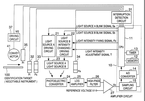
Referring to Fig. 1, reference numeral 10 denotes
a control unit for controlling the overall negotiable
instrument identifying apparatus of this embodiment. The
control unit 10 is comprised of a CPU 11 for performing
various control operations in accordance with control
procedures that are stored in, for example, a memory 12
and indicated by the flow charts to be described later,
the memory 12 storing control programs for the CPU 11
and the like, a timer 13 for performing time control, an
A/D converter 14 for converting an input analog signal
into a corresponding digital signal, and a sampling
circuit 15 for sampling an analog signal input through
an input port.
According to this embodiment, in the control unit
10, the CPU 11 outputs light source control data DD2 as
light source control signals (Sa, Sb, Fb, and T) upon
- 10 -
CA 02308644 2000-OS-17
detection of a first half end signal UDl from the timer
13, and outputs DD1 upon detection of UD2. Upon
detection of an A/D conversion start signal ADT, the CPU
11 controls the sampling circuit 15 and A/D converter 14
to start A/D conversion.
As a consequence, different light source driving
states based on DD1 and DD2 alternately occur at a
predetermined duty ratio, and a light-reception output
can always be sampled and loaded into the CPU 11 at a
predetermined time point in each cycle.
Reference numeral 21 denotes a light source A
driving circuit for performing blink control on the
light source A in accordance with a light source A blink
signal Sa; and 22, a light source B intensity
changing/driving circuit serving as an automatic
emission intensity adjusting circuit for the light
source B, which performs blink control on the light
source B in accordance with a light source B blink
signal Sb from the control unit 10, adjusts the emission
intensity of the light source B in accordance with a
light intensity adjustment signal T, and holds an
adjusted state by stopping light intensity adjustment
when a light intensity fixing signal Fb is output.
Reference numeral 23 denotes a light source
Alight source B capable of emitting light beams having
different wavelengths. Obviously, the light source A and
- 11 -
CA 02308644 2000-OS-17
light source B may be separate light-emitting elements,
or may be a composite light source formed by integrating
two light sources.
Reference numeral 24 denotes a photoelectric
converter for receiving light from the light source
Alight source B 23 or light transmitted through an
identification target 100, converting the received light
into an electrical signal corresponding to the amount of
light received, and outputting the signal, and it can be
formed by using photodiode and the like.
Reference numeral 25 denotes a log amplifier for
amplifying the electrical signal from the photoelectric
converter 24.
In this embodiment of the present invention, a
light-reception signal value from the photoelectric
converter 24 is amplified by the log amplifier 25 for
the following reason. If a linear amplifier is used, an
output from the linear amplifier always contains
absolute value components of emission intensity. When,
therefore, a linear amplifier is used, offsets
associated with absolute value components of emission
intensity, e.g., variations in the distance between the
light source and the photoelectric converter, emission
intensity, light-reception intensity, and the like,
temperature characteristics, deterioration, and the like,
cannot be basically removed. In contrast to this, when a
- 12 -
CA 02308644 2000-OS-17
log amplifier is used, an output associated with only
the properties of an identification target can be
obtained. In addition, since a method of obtaining the
difference in output between identical log amplifiers,
Is cancellation a.nd the like unique to log amplifiers
need not be performed, and the arrangement of a log
amplifier itself can be simplified.
Letting Ma and Mb be the emission intensities of
the light sources A and B, and N be a common steady
background, when a linear amplifier is used,
V~ ( Ma + N ) - ( Mb + N ) - Ma - Mb
When a log amplifier is used,
V~ln (Ma + N) - In (Mb + N) - ln{ (Ma + N) / (Mb + N) }
Assume that each emission intensity is
automatically adjusted to set the peak value to "0". In
this case, if a linear amplifier is used,
Ma - Mb = 0 ~ ~ ~ .~.Ma = Mb
When a log amplifier is used,
(Ma + N) / (Mb + N) - 1 ~ - ~ .~.Ma = Mb
As a consequence, the emission conditions in the above
two cases become the same.
In the above condition Ma = Mb (= C), if an
identification target exhibiting transmittances a and b
with respect to light beams from the two light sources
23 is present between the light source Alight source B
23 and the photoelectric converter 24, a peak value V is
- 13 -
CA 02308644 2000-OS-17
given by
Via ~ Ma - b ~ Mb = (a - b) C
when a linear amplifier is used. In this case, the
output contains an absolute value component C of
emission intensity. When a log amplifier is used,
V~ln{ (a ~ C + N) / (b ~ C + N) }
Under the condition of a~C, b~C ~~ N (N may not be
steady), the following output can be approximately
obtained:
V~ln{ (a ~ C) / (b ~ C) } - In (a/b)
The output representing only the properties of the
identification target can be obtained with some
conditions. For this reason, this embodiment of the
present invention uses a log amplifier.
Reference numeral 26 denotes a high-pass filter
for removing components having frequencies less than the
light source driving frequency (DC components and
fluctuation components associated with brightness which
are produced between the DC components and the light
source driving frequency) from a detection electrical
signal from the log amplifier 25; and 27, an amplifier
circuit for superimposing a DC voltage Vl as a reference
on the output from the high-pass filter 26, and
outputting the resultant voltage.
Reference numeral 31 denotes an interruption
detection circuit for detecting an identification target.
- 14 -
CA 02308644 2000-OS-17
The interruption detection circuit 31 drives sensors,
wave-shapes detection signals, and outputs the resultant
signals to the control unit 10. The control unit 10
detects the position of the identification target 100 on
the basis of detection signals Rck from identification
target sensors 32, 33, and 34 and rotation sensor (Pr)
35.
The input sensor (Pi) 32 detects the insertion of
the identification target 100. The identification start
sensor (Ps) 33 detects a reference for the position of
the identification target 100 and also detects that the
identification target 100 reaches the installation
position (detection area) of the light source 23 and
photoelectric converter 24. The pass sensor 34 detects
that the identification target 100 passes through the
installation position of the light source 23 and
photoelectric converter 24 and moves outside the
detection area.
The rotation sensor (pr) 35 detects the rotation
amount of a convey motor 41 (the convey amount of the
identification target 100). The rotation sensor (pr) 35
detects pulses Rck for the rotation amount of the convey
motor 41. These sensors 32 to 35 can be formed by using
photointerrupters and the like.
Reference numeral 37 denotes a driving circuit for
the convey motor 41. The driving circuit 37 drives the
- 15 -
CA 02308644 2004-09-16
convey motor 41 in accordance with a motor switch signal Ms
from the CPU 11 of the control unit 10. The convey motor 41
conveys the identification target 100.
The identification target 100 includes an arbitrary object
through which light is partly transmitted. In this embodiment,
a convey unit is designed for a sheet-like object as a target.
However, an identification target having an arbitrary shape can
be identified by only changing the structure of the convey
unit.
In this embodiment described above, the control unit 10 is
formed by using, for example, a one-chip microcomputer, which
is connected to an external unit through an I/O port to
simplify the hardware arrangement. If the control unit is
designed to directly A/D-convert a sampled value of an AC
output signal and load it as data into an identifying unit
formed by the CPU 11, in particular, the circuit can be
simplified.
The control unit 10 in this embodiment performs authenti-
cation as follows. The photoelectric converter 24 is adjusted
in advance such that the same output signal is obtained with
respect to the light sources A and B that emit light beams
having different wavelengths. Furthermore, the output signal of
photoelectric converter 24 is adjusted by the light intensit~~
of the light source B. The output difference between detection
-16-
CA 02308644 2000-OS-17
signals based on light beams transmitted through the
identification target in this state is detected as an
output from the high-pass filter 26. The sampling
circuit 15 then samples a signal proportional to the
difference in output between the detection values based
on the light sources A and B, which is based on this
output difference. Authentication is performed on the
basis of the sampled value.
The light source A blink signal Sa and light
source B blink signal Sb are used to control this
alternate emission. The light intensity adjustment
signal T is used to adjust each emission intensity. When
the identification target reaches a recognition area,
the above adjustment is not performed, and light
intensity is fixed. The light intensity fixing signal Fb
i~s a control signal for this operation.
In this embodiment, a deterioration in the light
sources is suppressed by periodically setting an
interval during which only emission is stopped while the
adjusted level is held in the absence of an
identification target, instead of continuing adjustment
by always alternately causing the light sources A and B
to emit light beams. This control will be described in
detail later.
Fig. 2 shows the detailed arrangement of the light
source B intensity changing/driving circuit 22.
- 17 -
CA 02308644 2000-OS-17
Referring to Fig. 2, in accordance with the light
source B blink signal Sb, the light source is
ON/OFF-controlled. Light source driving current control
is performed in accordance with the light intensity -
adjustment signal T. A light source driving current is
fixed in accordance with the light intensity fixing
signal Fb.
As shown in Fig. 2, an analog switch circuit is
used to perform adjustment stop control based on the
light intensity adjustment signal T when the light
intensity fixing signal Fb is output. This circuit is
integrally formed with a low-pass filter unit.
When the light intensity fixing signal Fb is "0",
the analog switching circuit is turned on. The output of
the low-pass filter unit shifts to a voltage lower than
the current voltage when the light intensity adjustment
signal T is "0", and shifts to a voltage higher than the
current voltage when the light intensity adjustment
signal T is "1".
A sample-and-hold unit serves only as a buffer
when the light intensity fixing signal Fb is "0", and a
change in output from the low-pass filter is directly
used as a control signal for a light source driving
current. As a consequence, when the current voltage
shifts to a lower voltage, the driving current for the
light source B increases.
- 18 -
CA 02308644 2000-OS-17
When the current voltage shifts to a higher
voltage, the driving current for the light source B
decreases. When the light intensity fixing signal Fb
becomes "1", since the analog switch circuit is opened,
the operational amplifier operates as a voltage hold
circuit. As a consequence, the control signal for the
light source driving current is fixed, and this state is
held.
Fig. 3 shows an example of the detailed
arrangement of the light source A driving circuit 21 in
Fig.. 1. As shown in Fig. 3, blinking of the light source
A is controlled in accordance with ON/OFF of the light
source A blink signal Sa.
According to the above description, the light
source A 21 and light source B 22 are formed by
light-emitting diodes having different arrangements.
However, the present invention is not limited to the
case wherein the light source A 21 and light source B 22
are formed by light-emitting diodes having different
arrangements. The light source A 21 and light source B
22 may be integrated into a composite light source.
Fig. 4 shows an example of the detailed arrangement of
the light source A driving circuit 21 and light source B
intensity changing/driving circuit 22 when they are
integrated into a composite light source.
In the circuit shown in Fig. 4, light-emitting
- 19 -
CA 02308644 2000-OS-17
diodes are formed by cathode-common two-color
light-emitting diodes. When the light source B blink
signal Sb is "0", both the light sources A and B are
turned off (non-emission state) regardless of the state
of the light source A blink signal Sa. When the light
source A blink signal Sa is "0" and the light source B
blink signal Sb is "1", the light source A is turned off
(no-emission state), and the light source B is turned on
(emission state). When the light source A blink signal
Sa is "1" and the light source B blink signal Sb is "1",
the light source A is turned on (emission state), the
light source B is turned off (no-emission state).
Assume that in the following description, the
light source A 21 and light source B 22 are formed by
separate light sources, and the light source A driving
circuit 21 and light source B intensity changing/driving
circuit 22 respectively have the arrangements shown in
Figs. 3 and 2. With the arrangement shown in Fig. 4,
these light sources can be treated in the same manner as
described above by changing the control timing of the
light source A blink signal Sa and light source B blink
signal Sb from the control unit 10.
Fig. 5 shows control data for the output port of
the CPU 11 which outputs four types of light source
control signals (each consisting of one bit). The values
of DD1 and DD2 are set in a control procedure to which
- 20 -
CA 02308644 2000-OS-17
the operation mode shifts. By alternately outputting
combinations of two values of DD1 and DD2 to the output
port, alternate control on the light sources which is
unique to each mode is performed. _
Fig. 5A shows control data set in a fixed emission
mode (detection mode); Fig. 5B, control data in an
adjustment emission mode (standby adjustment mode or
pre-detection adjustment mode) of adjusting emission
intensity; and Fig. 5C, control data set in a
non-emission mode (standby hold mode) unique to this
embodiment.
In the fixed emission mode shown in Fig. 5A, when
DD1 is output to the output port, the light source A
blink signal Sa becomes "1", and the light source B
blink signal Sb becomes "0". As a consequence, only the
light source A emits light. When DD2 is output to the
output port afterward, the light source A blink signal
Sa becomes "0", and the light source B blink signal Sb
becomes "1". As a consequence, only the light source B
emits light.
The light intensity fixing signal F becomes "1"
regardless of whether DD1 or DD2 is output. At this time,
the above analog switch circuit is open, and hence the
light intensities set when the circuit was opened are
fixed. As described above, in the fixed emission mode,
the two light sources alternately emit light beams while
- 21 -
CA 02308644 2000-OS-17
the light intensities are kept in a given state. In this
case, the light intensity adjustment signal T may be "1"
or "0" because its value does not influence the emission
condition.
In the adjustment emission mode shown in Fig. 5B,
when DDl is output to the output port, the light source
A blink signal Sa becomes "1", and the light source B
blink signal Sb becomes "0". As a consequence only the
light source A emits light. When DD2 is output to the
output port afterward, the light source A blink signal
Sa becomes "0", and the light source B blink signal Sb
becomes "1". As a consequence, only the light source B
emits light.
The light intensity fixing signal F becomes "0"
regardless of whether DDl or DD2 is output. At this time,
the above analog switch circuit is on. Therefore, while
"0" is output as the light intensity adjustment signal T,
the light intensity of the light source B decreases. In
contrast to this, while "1" is output as the light
intensity adjustment signal T, the light intensity of
the light source B increases. The degree of
increase/decrease in light intensity is determined by
the time constant of the low-pass filter unit.
In steps S112 and S113, the T-bit values of DD1
and DD2, each output as the light intensity adjustment
signal T, are updated and stored on the basis of the
- 22 -
CA 02308644 2000-OS-17
result obtained by comparing a sampled value of an
alternate output signal Vo with the reference voltage Vl
in step 5111 in the control procedure. These values are
updated and output at a subsequent alternate switching
timing.
Assume that a sampled value becomes small when the
light source B is dominant with respect to the light
source A as in this embodiment. In this case, if the
sampled value is smaller than the value of the reference
voltage Vl, T bits are set to "0" to decrease the light
intensity of the light source B. If the sample value is
larger than the value of the reference voltage Vl, T
bits are set to "1". As described above, in the
adjustment emission mode, light source intensity
adjustment is performed to always bring a sample value
in an alternate emission state near to the reference
value.
In the non-emission mode shown in Fig. 5C, the
light source A blink signal Sa, light source B blink
signal Sb, and light intensity fixing signal F are "0",
"0", and "1", respectively, regardless of whether DD1 or
DD2 is output, and hence the light sources A and B emit
no light. Since the analog switch circuit is open, a
voltage value for defining light intensity which was set
when the analog switch circuit was opened is fixed.
As described above, in the non-emission mode, the
- 23 -
CA 02308644 2000-OS-17
lightintensity level in non-emission state is kept
the
at certain level. In thiscase, the value thelight
a of
intensity adjustment signal T may be "1" or "0" because
its value does not influence the emission condition. _
In this embodiment, as described above, the light
sources can be controlled by alternately outputting DDl
and DD2.
General control operation in this embodiment
having the above arrangement will be described with
reference to Fig. 6. Fig. 6 is a flow chart showing
general control operation in this embodiment.
When the negotiable instrument identifying
apparatus of this embodiment is powered on,
predetermined initialization processing is executed
first, and then, the control operation shown in Fig. 6
starts. First of all, in step S100 standby adjustment
mode processing is executed to execute the adjustment
mode for a predetermined period of time. In this mode,
the light sources A and B alternately emit light beams,
and the detection levels of the photoelectric converter
24 are made uniform.
More specifically, the CPU 11 repeats a light
source driving cycle a predetermined number of times (60
times; a total of 15 msec, in this embodiment), in which
the light sources A and B alternately emit light beams,
the photoelectric converter 24 receives the light beams,
- 29 -
CA 02308644 2000-OS-17
and negative feedback control is performed to set the
value A/D-converted by the A/D converter 14 to a
specific value. Thereafter, the flow advances to step
5200 to execute the standby hold mode of stopping
emission control on the light sources A and B for a
predetermined period of time.
In the standby hold mode processing in step 5200,
the CPU 11 repeats a light source driving cycle a
predetermined number of times (8,000 times; a total of 2
sec, in this embodiment), in which the light intensity
fixing signal Fb is output to hold the emission
intensity level set when the flow shifted from the
standby adjustment mode in step S100, and alternate
emission is stopped in this state. Thereafter, the flow
returns to the standby adjustment mode in step 5100.
If the interruption of light is determined (the
insertion of the identification target 100 is detected)
by checking the detection state of the input sensor (Pi)
32 in every cycle in this standby hold mode, the flow
advances to the pre-detection adjustment mode in step
5300. Note that this detection state may be checked
every several cycles.
In step 5300, the CPU 11 executes the
pre-detection adjustment mode of causing the light
sources A and B to alternately emit light beams and
making the detection levels of the photoelectric
- 25 -
CA 02308644 2000-OS-17 .
converter 24 uniform. In the pre-detection adjustment
mode, the driving signal MS is output to the convey
motor 41 to drive the convey motor so as to start
conveying an identification target into the apparatus.
At the same time, the CPU 11 performs the same operation
as the standby adjustment mode in step S100 a
predetermined number of times (e. g., 60 times; a total
of 15 msec, in this embodiment). The flow then advances
to the detection mode in step 5400.
In the detection mode in step S400, the CPU 11
outputs the light intensity fixing signal Fb to hold the
emission intensity level set when the flow advances from
the pre-detection adjustment mode in step 5300. While
this state is held, the light sources A and B
alternately emit light beams, and the sampling circuit
15 samples the output Vo from the amplifier circuit 27
in every cycle. In addition, the CPU 11 determines the
current state by checking Pi 32, Ps 33, Pe 34, and Pr 35
in every cycle. After the CPU 11 repeats this operation
a predetermined number of times (8,000 times or less in
this embodiment), the flow returns to the standby
adjustment mode in step 5100.
If no identification target is detected after a
lapse of a predetermined period of time in the standby
hold mode processing in step S200, the flow advances to
the processing in step S100 after a lapse of a
- 26 -
CA 02308644 2000-OS-17
predetermined period of time. The CPU 11 then
alternately executes the processing in step S100 and the
processing in step 5200.
With this operation, the CP_U 11 stops light
emission during the execution of the processing in step
5200 instead of always alternately causing the light
sources A and B to emit light beams, thereby suppressing
a decrease in the service life of each light source. In
this embodiment, the control operation shown in Fig. 6
and driving control on the convey motor 41 (to be
described in detail later) are switched every time the
count value of a counter Mct for counting light source
driving cycles reaches a predetermined count value.
Fig. 7 shows the count value of the counter Mct
and each operation control switching timing. Fig. 7 is a
timing chart showing the operation of this embodiment.
The upper, intermediate, and lower portions of Fig. 7
respectively indicate the counter value of the counter
Mct, the respective operation modes in Fig. 6, and the
control timing of the convey motor 41 and light sources.
The execution of the standby hold mode is started
when the Mct count value becomes Swkl, and is kept
executed until the count value becomes Swk2. When the
Mct count value becomes Swk2, the flow advances to the
standby adjustment mode, and the Mct count value is set
to Swtl. This mode is executed until the Mct count value
- 27 -
CA 02308644 2000-OS-17
becomes Swt2. During this period, the light intensity
fixing signal Fb is set to be adjustable, and the light
sources A and B alternately emit light beams to perform
light intensity adjustment. -
When the Mct count value becomes Swt2, the Mct
count value is preset to Swkl, and the flow advances to
the standby hold mode. If the input sensor (Pi) 32
detects the insertion of an identification target in the
above standby hold mode, the flow advances to the
pre-detection adjustment mode while presetting the Mct
count value to Sdtl to drive the convey motor 41 so as
to convey the identification target to the
identification area. During this period, the light
intensity fixing signal Fb is set to be adjustable, and
the light sources A and B alternately emit light beams,
thereby performing light intensity adjustment.
When the Mct count value becomes Sdt2, the
pre-detection adjustment mode is terminated, and the
detection adjustment result is fixed. The Mct count
value is then preset to Sdcl to start the detection mode.
The CPU 11 keeps driving the convey motor 41 to convey
the identification target to the identification area,
and waits for the arrival of the identification target
at the position of the identification start sensor (Ps)
33. If the interruption of light is detected, a counter
Ect for counting pulse signals Rck generated by the
- 28 -
CA 02308644 2000-OS-17
rotation sensor (Pr) 35 starts counting.
Subsequently, the properties of the identification
target are obtained to perform determination by checking
the sampled value of the reception output Vo and the
position of the identification target specified by the
count value of the counter Ect in correspondence with
each other.
When the identification target passes the position
of the identification end sensor (Pe) 34, the detection
mode is terminated, and the Mct count value is preset to
Swtl. The flow then advances to the standby adjustment
mode.
Fig. 8 shows examples of the set values of the Mct
count values in the respective modes. Referring to
Fig. 8, "initial value (Mci)" is a preset value at the
start of the execution of mode processing, "preset 2
(Mp2)" is an Mct count value at the time of the end of
mode processing, and "preset 1 (Mpl)" indicates the
alternate switching timing of the light sources A and B,
which will be described later. "preset 1 (Mpl)" is the
count value that shows the switching timing of the first
adjustment and second adjustment described in the second
embodiment. Note that the switching control table shown
in Fig. 8 is stored in the memory 12.
A detailed control example in this embodiment in
setting the Mct count values shown in Fig. 8 will be
- 29 -
CA 02308644 2000-OS-17
described below with reference to Fig. 9. Fig. 9 is a
flow chart showing operation in a light source driving
cycle in this embodiment. Fig. 10 is a timing chart
showing the relationship between the light source
driving cycle and a signal generated by a timer and sent
to the CPU in this embodiment. Referring to Fig. 9,
reference symbol Mct denotes a counter incremented in
every light source driving cycle. The value of the
counter Mct is set to fall within a specific range in
each operation mode. Each mode can therefore be
identified by only checking the value of the counter Mct.
Referring to Fig. 9, light source A driving
control in the first half period is performed in steps
Sl to step S5. More specifically, the flow returns to
step Sl if it is determined in step Slb in the previous
cycle that a second half end signal is "1" (UD2 = "1").
In step S1, as shown in Fig. 5 DDl is output to the
output port (DD) to switch from the light source B
driving state to the light source A driving state. UD2
is reset to "0". In step S2, the first processing (to be
described in detail later) is executed. In this case, if
sampling and A/D conversion are started in the second
half period of the previous cycle, evaluation of
conversion data, determination, processing, and the like
are performed.
In step S3, the Mct counter is incremented by one
- 30 -
CA 02308644 2000-OS-17
to count the number of times this light source driving
cycle is executed. In step S4, the CPU 11 checks UDl =
"0" indicating that the first half period has not ended.
_ The flow then advances to step S5 in a first half end
signal wait loop to check whether UD1 = "1".
If UD1 = "1", the flow advances to the processing
in step S11 and subsequent steps, and advances to the
light source B driving control in the second half period.
In step 511, DD2 is output to DD to switch from the
light source A driving state to the light source B
driving state. UDl is reset to "0" in advance. The flow
then advances to step S12 to execute mode selection
state check processing, thereby performing mode
continuation or shift determination corresponding to
each operation mode, initialization upon shift, a check
on the position of the identification target, and the
like.
In step S13, the second process is executed. In
case that the present cycle is in need of setting A/D
conversion, a conversion start signal is output to the
sampling circuit 15 and A/D converter 14 at a
predetermined timing after a preparation for conversion
is made. In step S19, the CPU 11 confirms that UD2 is
"0". In step 515, the CPU 11 monitors whether UD2
changes to "1". If UD2 becomes "1", the flow returns to
step Sl to perform emission control on the light source
- 31 -
CA 02308644 2000-OS-17
A.
The timer 13 periodically outputs the first half
period end signal UD1 associated with the light source
driving cycle, the second half period end signal UD2
thereof, and an A/D conversion start signal ADT to the
CPU 11 with predetermined time lags being kept among the
respective signals. In this embodiment, as shown in
Fig. 10, when the count value of a counter Gct for
counting original oscillation clock signals (f = 16 MHz)
reaches predetermined count values GD1, GD2, and GAD,
UD1, UD2, and ADT change from "0" to "1". In the case of
GD2, the counter Gct is reset to continue a series of
operations.
More specifically, GD1 = 2,000, GD2 = 4,000, and
GAD = 3950 are set to obtain a light source driving
cycle of 4 kHz (= 16 MHz/4,000) and an A/D conversion
timing generated in the second half period in
synchronism with the light source driving cycle. Note
that UD1, UD2, and ADT are reset from "1" to "0" under
the control of the CPU 11 after they are detected by the
CPU 11.
Fig. 11 shows the first process in step S2 in
Fig. 9 in detail. In the first process, first of all it
is checked in step 5101 whether the Mct count value is
equal to or less than "40,000", which indicates a mode
other than the discharge or standby hold mold. If the
- 32 -
CA 02308644 2000-OS-17
count value is not equal to or less than "40,000", since
the standby hold mode is set, and no A/D conversion data
needs to be loaded, the flow returns.
If it is deter-mined in step 5101 that the Mct
count value is equal to or less than "40,000" , the
detection mode and each adjustment mode are set, and a
value has been sampled and A/D conversion has been
started in step 513. The flow therefore advances to step
S102. If the end of conversion is confirmed by checking
the conversion end signal, the flow advances to step
S103.. In step 5103, the data from the A/D converter 19
is loaded into the CPU 11.
In step S104, whether the Mct count value is equal
to or more than "10,000" is checked to determine whether
the light intensity adjustment mode or detection mode is
set.
If the Mct count value is "10,000" or less, it
indicates that the detection mode is being executed. In
step S105, it is checked whether a confirmation signal
Fjp is stored. The confirmation signal Fjp is a marker
indicating that the position of the identification
target 100 can be specified. In step S53 (to be
described in detail later), the confirmation signal Fjp
is stored or set when a predetermined clock change of
the pulse output Rck from the rotation sensor (Pr) 35 is
confirmed between the previous light source driving
- 33 -
CA 02308644 2000-OS-17
cycle and the current cycle. If there is no confirmation
signal Fjp, it is determined that the identification
target 100 is not located at a position where its
position should be determined, and the flow returns
without performing determination.
If it is determined in step S105 that the
confirmation signal Fjp is present, the flow advances to
step S106 to count Rck and increment Ect by one. In step
5107, determination processing is executed at the
corresponding point, and the flow returns.
If it is determined in step S104 that the Mct
count value is "10,000" or more, the flow advances to
step 5111 to compare the A/D-converted data value of the
AC output signal Vo loaded in step 5103 with a
predetermined digital value corresponding to the
reference voltage V1. If the reference voltage Vl is
higher, the flow advances to step 5112 to set the T bits
of DD1 and DD2 to "0" to make a preparation for
decreasing the light intensity of the light source B.
The flow then returns.
If it is determined in step S111 that the
reference voltage V1 is lower, the flow advances to step
S113 to set the T bits of DDl and DD2 to "1" to make a
preparation far increasing the light intensity of the
light source B. The flow then returns.
Fig. 12 shows the detailed second process in step
- 39 -
CA 02308644 2000-OS-17
S13 in Fig. 9. In the second process, first of all it is
checked in step S131 whether the Mct count value is
"40,000" or less which indicates a mode other than the
discharge or standby hold mode shown in Fig. 8. If the
Mct count value is not "40,000" or less, since it
indicates that the standby hold mode is set, the flow
returns without performing A/D conversion.
If it is determined in step 5131 that the Mct
count value is "40,000" or less, since it indicates that
a mode in which A/D conversion should be performed is
set, the flow advances to step 5132. It is then
confirmed that the ADT signal is "0" before the A/D
conversion timing in Fig. 10, and a preparation for A/D
conversion processing is made.
In step S133, the CPU 11 monitors whether the A/D
conversion timing has come, and the ADT signal becomes
"1". If the A/D conversion timing has come, and the ADT
signal becomes "1", the flow advances from step 5133 to
step S134 to output a conversion start signal to the
sampling circuit 15 and A/D converter 14. The ADT signal
is then set to "0", and the flow returns.
The mode selection state check processing in step
S12 in Fig. 9 will be described in detail with reference
to Figs. 13A and 13B.
In the mode selection state check processing in
step 512, first of all it is checked in step S51 whether
- 35 -
CA 02308644 2000-OS-17
the Mct count value is 10,000 or more, i.e., the
detection mode is set. If the Mct count value is not
10,000 or more, since the detection mode is set, the
- flow advances to step S52 to check whether the Ps 33 or
Pe 34 has detected the identification target 100, i.e.,
the identification target 100 is located in the
identification area.
If it is determined in step S52 that the Ps 33 or
Pe 34 has detected the identification target 100, the
flow advances to step S53 to check the Pr 35 and compare
its current value with the value detected by the Pr 35
and stored in the previous cycle. If a predetermined
change in value is determined, it is determined that the
identification target 100 has been conveyed by a
predetermined amount. In this case, it is determined
that a cycle in which the position of the identification
target 100 can be specified is set, and the confirmation
signal Fjp is stored. In addition, the value detected by
the Pr 35 and stored in the previous cycle is updated to
the detection value in the current cycle.
If it is determined in step S52 that neither the
Ps 33 nor the Pe 34 have detected the identification
target 100, it is determined that the identification
target has not reached the position of the
identification start sensor (Ps) 33. The flow then
advances to step S54 to reset the counter Ect to "0",
- 36 -
CA 02308644 2000-OS-17
which counts Pr signals for specifying the position of
the identification target from the identification start
position.
In step X55, it is checked whether the input
sensor Pi 32 has detected the identification target. If
the input sensor Pi 32 has detected the identification
target, it is determined that the leading edge of the
identification target is located between the Pi 32 and
the Ps 33. Thereafter, the identification target is
conveyed upon rotation of the convey motor 41 and
reaches the position of the Ps 33. The flow therefore
advances to step 553.
If it is determined in step S55 that the input
sensor Pi 32 has not detected the identification target,
since a detection error may be present in the input
sensor, the flow advances to the standby hold mode in
step S60 and the subsequent steps. In step S60, the
count value of the Mct count value is set to 40,000, and
preset 2 (Mp2) is set to 98,000. In step 562, the MS
signal is turned off to perform control so as not to
drive the convey motor 41. In step 563, DDl and DD2 as
driving pulse data putputs are set to non-emission data.
The flow then returns.
If it is determined in step S51 that the Mct count
value is 10,000 or more, since the detection mode is not
set, the flow advances to step S71 to check whether the
- 37 -
CA 02308644 2004-09-16
Mct count value is 40,000 or more, i.e., an operation mode in
which the light sources are not turned on, e.g., the standby
hold mode, is set. If the Mct count value is not 40,000 or
more, since the standby adjustment mode or pre-detection
adjustment mode is set, the flow advances to step S72 to check
whether the Mct count value is equal to preset 2 (Mp2). If the
Mct count value is not equal to preset 2 (Mp2), since it
indicates that the adjustment mode has not been completed, the
flow returns.
If the Mct count value becomes equal to preset 2 (Mp2),
the flow advances to step 573. If the Mct count value is 20,000
or less, and the pre-detection adjustment mode is set, the
detection mode in step S75 and the subsequent steps is started.
In step 576, the count value of the counter Mct is reset
to "0", and preset 2 (Mp2) is set to 8,000 to execute the
detection mode afterward. In order to insert the identification
target 100 into the apparatus, the MS signal is enabled to
continuously drive the convey motor 41, which has already been
driven, in step 577. DD1 and DD2 as driving pulse data outputs
are then set to fixed emission data. The flow then returns.
With this operation, the emission intensities are fixed, and
the identification target passes through the identification
area.
If it is determined in step S73 that the Mct count
-38-
CA 02308644 2000-OS-17
value is not 20,000 or less, since it indicates that the
standby adjustment or initialization adjustment is
performed, the flow advances to the standby hold mode in
step S60 and the subsequent steps. When this processing
is complete, the Mct count value is set to 40,000, and
preset 2 (Mp2) is set to 48,000 to shift to the hold
mode. In step S62, the MS signal is turned off
(disabled) to stop the convey motor 41. DD1 and DD2 as
driving pulse data outputs are set to non-emission data.
The flow then returns.
If it is determined in step S71 that the Mct count
value is 40,000 or more, it indicates that the standby
hold mode or discharge mode is being executed. The flow
then advances to S81 to check whether light received by
the input sensor (Pi) is interrupted, and an
identification target is inserted into the apparatus. If
light received by the input sensor (Pi) is not
interrupted, the flow advances to step S82 to check
whether the Mct count value becomes equal to preset 2
(Mp2), and the operation under execution is complete. If
the Mct count value is not equal to preset 2 (Mp2), the
flow returns.
If it is determined in step S82 that the Mct count
value is equal to preset 2 (Mp2), the flow advances to
the standby adjustment mode in step S85 and the
subsequent steps. In step 586, the Mct count value is
- 39 -
CA 02308644 2000-OS-17
set to 20,000, and preset 2 (Mp2) is set to 20,060. In
step S87, the MS signal is turned off (disabled) to stop
the convey motor 41. In step 588, DD1 and DD2 as driving
pulse data outputs are set to adjustment emission-data.
The flow then returns.
If it is determined in step S81 that light
received by the input sensor (Pi) is interrupted, and an
identification target is inserted into the apparatus,
the Mct count value is set to 10,000 and preset 2 (Mp2)
is set to 10,060 to shift to the pre-detection
adjustment mode in step S91 and the subsequent steps. In
step S93 the MS signal is turned on to drive the convey
motor 41 to insert the identification target into the
apparatus, and pre-detection adjustment is executed at
the same time. In step 588, DD1 and DD2 as driving pulse
data outputs are set to adjustment emission data. The
flow then returns.
Fig. 14 shows examples of driving control signals
and detection signal timings for the light source
Alight source B 23 in the detection mode and standby
hold mode in the above control. Fig. 15 shows examples
of driving control signals and detection signal timings
for the light source Alight source B 23 in the standby
adjustment mode and pre-detection adjustment mode. Note
that the detection output Vo is indicated in opposite
phase to become lower than the reference voltage Vl when
- 40 -
CA 02308644 2000-OS-17
one light source that is dominant with respect to the
other light source emits light.
Identification control for an identification
target in this embodiment of the present invention,
which has the above arrangement, will be described below.
In this embodiment, control operation is performed to
set a detection output sampled value to the reference
voltage V1 before an identification target reaches the
detection range. The output of the log amplifier 25 at
the sampling timing is also controlled to a
predetermined voltage.
When the identification target reaches the
detection range while the amounts of light beams emitted
from the light source Alight source B 23 in this
control state are fixed, the photoelectric converter 24
outputs an electrical signal corresponding to the
wavelength of light emitted from each light source 23
and having passed through the identification target.
This signal is amplified by the log amplifier 25 and
output to the high-pass filter 26.
The waveform of the output Vo in Fig. 14 and 15 is
opposite in phase to a change in light amount. For this
reason, if, for example, the color of the identification
target in the detection range is reddish rather than
greenish (the transmittance degree of light from the
light source A is higher) when the light source A is a
- 41 -
CA 02308644 2000-OS-17
red and the light source B is a green the output voltage
of a signal at the light source A emission timing
becomes smaller than that of a signal at the light
source B emission timing in the case shown in Fig. 14.
In contrast to this, if the identification target in the
detection range is greenish rather than reddish (the
transmittance degree of light from the light source B is
higher), the output voltage value of a signal at the
light source B emission timing becomes smaller than that
of a signal at the light source A emission timing.
Referring to Fig. 14, at the timing when light
source A is dominant that is the Sa signal output timing,
the color of the identification target in the detection
range is reddish rather than greenish, and hence the
output voltage value of a signal at the light source A
emission timing is smaller than that of a signal at the
light source B emission timing. At the timing when the
light source B is dominant that is the Sb signal output
timing, the color of the identification target in the
detection range is greenish rather than reddish, and
hence the output voltage value of a signal at the light
source B emission timing is smaller than that of a
signal at the light source A emission timing.
The high-pass filter 26 removes components having
frequencies less than the light source driving frequency
from a detection signal to extract only AC components
- 42 -
CA 02308644 2004-09-16
having frequencies equal to or higher than the light source
driving frequency. The amplifier circuit 27 amplifies the light
source driving frequency and superimposes the reference vo:Ltage
V1 on the extracted components. The sampling circuit 15 samples
waveform data at the detection timing (second half period of a
light source driving cycle) of light emitted from the light
source B from this superimposed waveform. The A/D converter 7_4
A/D-converts the sampled data. The resultant data is stored in
the form of a digital value until the next A/D conversion.
In this embodiment, the amplifier circuit 27 outputs a
signal that oscillates to the positive or negative side with
respect to the reference voltage V1 in proportion to changes
(the difference between detection signals when the
photoelectric converter 24 receives light beams from the two
light sources) in the amounts of light beams detected from the
light sources A and B. For example, therefore, the extent to
which the color of an identification target is reddish (when
the signal oscillates to the positive side) or the extent to
which the color of an identification target is greenish (when
the signal oscillates to the negative side) can be detected by
only sampling a signal at the detection timing of light emitt=ed
from the light source B.
As a consequence, there is no need to perform
-43-
CA 02308644 2000-OS-17
identification for each of a plurality of colors in
authenticating an identification target such as a
negotiable instrument (to be described later), and a
_ specific one of the colors which has the highest density
can be determined by only determining one type of
detection signal. This makes it possible to greatly
simplify the arrangement of the apparatus.
The CPU 11 loads the signal level of a detection
signal change (color appearance and degree) caused upon
switching from the light source A to the light source B,
which is the sampling result obtained by the sampling
circuit 15. As shown in Fig. 14, in this embodiment the
tendency of the color of an identification target with
respect to light beams emitted from the light source
Alight source B 23 is output as one signal.
The CPU 11 therefore compares this detection
signal pattern with the standard pattern obtained by
detecting an authentic identification target (negotiable
instrument or the like) and registered in the memory 12
in advance at predetermined convey intervals, thereby
determining the degree of similarity. If a predetermined
degree of similarity or higher is determined, the
identification target is identified as an authentic one.
It suffices if one type of standard pattern is
held to be compared for each type of identification
target (e. g., a negotiable instrument or bill).
- 44 -
CA 02308644 2000-OS-17
Identification processing can therefore be simplified.
In addition, even comparison with only one type of
standard pattern can cope with a plurality of types of
color errors and can properly cope with almost all color
errors.
Even if, therefore, a bill image is printed on
only one surface of a sheet which should have bill
images printed on the two surfaces, or bill images are
copied on the two surfaces of a sheet or a bill image is
copied on one surface of a sheet by using a copying
machine, authentication can be properly performed.
Figs. 16 and 17 show sampling results with respect
to a predetermined identification target (using a proper
color chart) in this embodiment. Fig. 16 shows the
sampling result obtained with respect to the
identification target when green and red light-emitting
diodes are respectively used as the light sources A and
B.
Fig. 17 shows the sampling result obtained with
respect to the identification target when an infrared
light-emitting diode and red light-emitting diode are
respectively used as the light sources A and B. In this
case, although whether the identification target is
reddish, bluish, or greenish, i.e., a color arrangement,
cannot be accurately determined, high-sensitivity
detection can be performed within the green gamut.
- 45 -
CA 02308644 2000-OS-17
As described above, according to this embodiment,
there is provided a light-transmitting object
identifying apparatus which can automatically solve
problems associated with variations in performance of
each constituent member of a mechanism for detecting an
identification object, changes in performance over time,
and changes in performance due to environments with a
simple arrangement, can be easily manufactured and
adjusted, and has high reliability.
In addition, since the difference in color taste
between an authentic object and an identification target
can be expressed as a single signal with respect to the
identification target, reliable authentication can be
performed using a simple algorithm.
Furthermore, a deterioration in the light sources
can be minimized because the apparatus is designed to
perform detection sensitivity adjustment at
predetermined intervals and inhibit the light sources
from emitting light while no adjustment is performed, in
the absence of an identification target, instead of
performing adjustment by always causing the light
sources to emit light.
[Second Embodiment]
According to the above description, the light
source 23 has two light sources, and the photoelectric
converter 24 is used to detect light beams emitted from
- 46 -
CA 02308644 2000-OS-17
the two light sources and transmitted through an
identification target. However, the present invention is
not limited to the above arrangement. Obviously, the
_ _ light source may be constituted by a plurality of light
sources. For example, the light source A may be
constituted by light sources A1 and A2.
In this case, the emission intensities of the
light sources can be made uniform by using a method of
adjusting the emission intensities of the light sources
Al and A2 by causing them to emit light beams at a
timing B while the emission of the light source B is
stopped, and then adjusting the light source A
(constituted by the light sources A1 and A2) and the
light source B after returning the emission timing of
the light source A2 to a timing A. Since the adjustment
can be realized by the same operation as that described
above except for switching of the light source driving
circuit, the circuit arrangement can be simplified.
For example, the use of a composite light source
constituted by green and infrared LEDs and a red LED
makes it easy to detect bluish and greenish colors as
compared with the case wherein green and red LEDs are
used.
The second embodiment of the present invention, in
which a light source is constituted by a plurality of
light sources, will be described below. The same
_ 97 _
CA 02308644 2000-OS-17
reference numerals as in the first embodiment denote the
same parts in the second embodiment described below, and
a detailed description thereof will be omitted.
Fig. 18 shows the arrangement of a negotiable
instrument identifying apparatus according to the second
embodiment of the present invention. The second
embodiment shown in Fig. 18 includes a light source Al
driving circuit 121 having an arrangement similar to
that of the light source A driving circuit 21 in the
first embodiment shown in Fig. l, and differs from the
first embodiment in that the second embodiment also
includes a light source A2 intensity changing/driving
circuit 122 and a composite light source 123 constituted
by light sources Al, A2, and B. As output control
signals from the output port of a CPU 11, a light source
A1 blink signal Sal similar to the light source A blink
signal Sa, light source A2 blink signal Sa2, and light
intensity fixing signal Fa2 are prepared.
In the second embodiment, when a light source is
constituted by a plurality of light sources, for example,
the light source A shown in Fig. 18 is made of light
sources Al and A2, the light source A2 is caused to emit
light at the timing of the light source B to adjust the
emission intensities of the light sources A1 and A2
while the emission of the light source B is stopped in
the first adjustment emission.
- 48 -
CA 02308644 2000-OS-17
The emission intensities of the composite light
source can be made uniform by using the method of
adjusting the emission intensities of the light sources
A1 and A2 first, restoring the timing of the light
source A2 to that of the light source A after the second
adjustment emission process, and then adjusting the
light source A (constituted by the light sources A1 and
A2). In addition, since the adjustment can be realized
by the same operation as that in the first embodiment
except for switching of the light source driving circuit,
the circuit arrangement can be simplified.
Figs. 19A to 19D show control data for the output
port of the CPU 11, which outputs six types of light
source control signal (each consisting of one bit) in
the second embodiment. The values of DD1 and DD2 are set
in a control procedure to which the operation mode
shifts. By alternately outputting combinations of two
values of DD1 and DD2 to the output port, alternate
control on the light sources which is unique to each
mode is performed.
Fig. 19A shows control data set in a fixed
emission mode (detection mode); Fig. 19B, control data
in the first adjustment emission mode (standby
adjustment mode or pre-detection adjustment mode) of
adjusting emission intensity; Fig. 19C, control data in
the second adjustment emission mode (standby adjustment
- 49 -
CA 02308644 2000-OS-17
_ mode or pre-detection adjustment mode) of adjusting
emission intensity; and Fig. 19D, control data set in a
non-emission mode (standby hold mode).
In the fixed emission mode shown in Fig. 19A, when
DDl is output to the output port, the blink signals Sal
and Sa2 for the light sources A1 and A2 become "1", and
the light source B blink signal Sb becomes "0". As a
consequence, the light sources A1 and A2 emit light.
When DD2 is output to the output port afterward, the
blink signals Sal and Sa2 for the light sources Al and
A2 become "0", and the light source B blink signal Sb
becomes "1". As a consequence, only the light source B
emits light.
The light intensity fixing signals Fa2 and Fb
become "1" regardless whether DD1 or DD2 is output, and
the analog switch circuit described above is open at
this time. Therefore, the light intensities set when the
analog switch circuit was opened are fixed. As described
above, in this mode, the light source A (constituted by
the light sources Al and A2) and the light source B are
caused to alternately emit light while certain light
intensities are fixed. In this case, the value of the
light intensity adjustment signal T may be either "1" or
"0" because it does not influence the emission condition.
In the first adjustment emission mode shown in
Fig. 19B, when DDl is output to the output port, the
- 50 -
r
CA 02308644 2000-OS-17
light source A1 blink signal Sal, light source A2 blink
signal Sa2, and light source B blink signal Sb
respectively become "1", "0", and "0". As a consequence,
only the light source Al emits light. When DD2 is output
to the output port afterward, the light source A1 blink
signal Sal, light source A2 blink signal Sa2, and light
source B blink signal Sb respectively become "0", "1",
and "0". As a consequence, only the light source A2
emits light.
The light intensity fixing signal Fb is "1"
regardless of whether DD1 or DD2 is output, and, hence
the light source B keeps its light intensity level while
stopping light emission. The light intensity fixing
signal Fa2 is "0" regardless of whether DD1 or DD2 is
output, and the above analog switch circuit is on at
this time. For this reason, while "0" is output as the
light intensity adjustment signal T, the light intensity
of the light source A2 decreases. In contrast to this,
while "1" is output, the light intensity of the light
source A2 increases.
As described above, in the first adjustment
emission mode, the light source B holds its light
intensity level while stopping light emission, and
intensity adjustment of the light source A2 is performed
to always bring sampled values near to a reference value
while the light sources A1 and A2 are caused to
- 51 -
CA 02308644 2000-OS-17
alternately emit light. -
In the second adjustment emission mode shown in
Fig. 19C, when DD1 is output to the output port, the
light source A1 blink signal Sal, light source A2 blink
signal Sa2, and light source B blink signal Sb
respectively become "1", "1", and "0". As a consequence,
both the light sources A1 and A2 emit light.
When DD2 is output to the output port afterward,
the light source A1 blink signal Sal, light source A2
blink signal Sa2, and light source B blink signal Sb
respectively become "0", "0", and "1". As a consequence,
only the light source B emits light.
The light intensity fixing signal Fa2 is "1"
regardless of whether DDl or DD2 is output, and hence
the light intensity of the light source A2 is fixed. The
light intensity fixing signal Fb is "0" regardless of
whether DD1 or DD2 is output, and the above analog
switch circuit is on at this time. For this reason,
while "0" is output as the light intensity adjustment
signal T, the light intensity of the light source B
decreases. In contrast to this, while "1" is output, the
light intensity of the light source B increases.
As described above, in the second adjustment
emission mode, intensity adjustment of the light source
B is performed to always bring sampled values near to a
reference value while the light sources A and B
- 52 -
r
CA 02308644 2000-OS-17
constituting the composite light source whose light
intensity ratio is fixed are caused to alternately emit
light.
In the non-emission mode shown in Fig. 19D, each
of the light source Al blink signal Sal, light source A2
blink signal Sa2, and light source B blink signal Sb
becomes "0" regardless of whether DD1 or DD2 is output.
As a consequence, light emission is kept stopped. Each
of the light intensity fixing signals Fa2 and Fb becomes
"1" regardless of whether DD1 or DD2 is output, and the
above analog switch circuit is open. The voltage values
for defining light intensities which were set when the
analog switch circuit was opened are fixed.
As described above, in the non-emission mode, a
certain light source level is held in a non-emission
state. In this case, the light intensity adjustment
signal T may be "1" or "0" because its value does not
influence the emission condition.
As described above, the light sources can be
controlled by alternately outputting DDl and DD2.
The general control in the second embodiment
having the above arrangement is the same as that in the
first embodiment except for mode selection state check
processing. The mode selection state check processing in
the second embodiment will be described with reference
to Figs. 20A and 20B.
- 53 -
CA 02308644 2000-OS-17
In the mode selection state check processing shown
in Figs. 20A and 20B, first of all it is checked in step
S201 whether a Mct count value is equal to or larger
than 50,000, i.e., the discharge mode is set. If the Mct
count value is not 50,000 or more, the flow advances to
step 5202 to check whether the Mct count value is 10,000
or more.
If the Mct count value is not 10,000 or more, the
flow advances to step 5203 to check whether the Mct
count value is equal to the value of preset 2 (Mp2). If
the Mct count value is not equal to the value of preset
2 (Mp2), the flow advances to step 5204 to check whether
a Ps 33 or Pe 34 has detected an identification target
100, i.e., the identification target 100 is in the
identification area.
If the Ps 33 or Pe 34 has detected the
identification target 100, the flow advances to step
5210 to check a Pr 35 and compare the current value with
the detection value stored in the Pr 35 in the previous
cycle. If there is a predetermined change, it is
determined that the identification target 100 has been
conveyed by a predetermined amount. In this case, the
current cycle is determined as a cycle in which the
position of the identification target 100 can be
specified, and a confirmation signal Fjp is stored. In
addition, the detection value stored in the Pr 35 in the
- 54 -
CA 02308644 2000-OS-17
- previous cycle is updated to the detection value in the
current cycle, and the flow returns.
If it is determined in step 5204 that neither the
Ps 33 nor the Pe 34 have detected the identification
target 100, it is determined that the identification
target has not reached the position of the
identification start sensor (Ps) 33. The flow then
advances to step 5205 to reset a counter Ect for a Pr
signal for specifying the position of the identification
target from the identification start position to 0. In
step S206, it is checked.whether the input sensor Pi 32
has detected the identification target.
If it is determined in step S206 that the input
sensor Pi 32 has not detected the identification target,
since a detection error may be caused in the input
sensor, the flow advances to the standby hold mode in
step 5207 and the subsequent steps. In step 5207, the
count value of the counter Mct is set to 40,000, and
preset 1 (Mpl) and preset 2 (Mp2) are respectively set
to 60,000 and 48,000. In step 5208, an MS signal is
turned off to inhibit a convey motor 41 from being
driven. In step S209, DD1 and DD2 as driving pulse data
outputs are set to non-emission data, and the flow
returns.
If it is determined in step 5206 that the input
sensor Pi 32 has detected the identification target, it
- 55 -
CA 02308644 2000-OS-17
is determined that the leading edge of the
identification target is located between the Pi 32 and
Ps 33. Since the identification target is conveyed upon
rotation of the convey motor 41 and reaches the position
of the Ps 33, the flow advances to step S210. In step
5210, the Pr 35 is checked, and the current values is
compared with the detection value stored in the Pr 35 in
the previous cycle. If there is a predetermined change,
it is determined that the identification target 100 has
been conveyed by a predetermined amount. In this case,
the current cycle is determined as a cycle in which the
position of the identification target can be specified,
and the confirmation signal Fjp is stored.
In addition, the detection value stored in the Pr
35 in the previous cycle is updated to the detection
value in the current cycle, and the flow returns.
If it is determined in step 5202 that the Mct
count value is 10,000 or more, the flow advances to step
5212 to check whether the Ps 33 or Pe 34 has detected
the identification target 100, i.e., the identification
target 100 is in the identification area. If the Ps 33
or Pe 34 has detected the identification target 100 in
such situation other than the detection mode, the flow
advances to the discharge mode processing in step 5213
and the subsequent steps. In the discharge mode
processing, first of all in step S213 the count value of
- 56 -
CA 02308644 2000-OS-17
the counter Mct, preset 1 (Mpl), and preset 2 (Mp2) are
respectively set to 50,000, 60,000, and 58,000. In step
5214, the MS signal is turned on to drive the convey
motor 41 to convey the identification target and
discharge it from the discharge position. In step 5209,
DD1 and DD2 as driving pulse data outputs are set to
non-emission data. The flow then returns.
If it is determined in step 5212 that neither the
Ps 33 nor the Pe 34 have detected the identification
target 100, the flow advances to step S215 to check
whether the Mct count value is 40,000 or more, i.e., the
standby hold mode of inhibiting the light sources from
emitting light is set. If the Mct count value is not
40,000 or more, since the standby adjustment mode or
detection mode is set, the flow advances to step S216 to
check whether the Mct count value is equal to the value
of preset 1 (Mpl). If the Mct count value is equal to
the value of preset 1 (Mpl), the flow advances to the
second adjustment mode in the step S222 to set
adjustment emission data as the driving pulse data DD1
and DD2. The flow then returns.
If it is determined in step 5216 that the Mct
count value is not equal to the value of preset 1 (Mpl),
the flow advances to step 5217 to check whether the Mct
count value is equal to the value of preset 2 (Mp2). If
the Mct count value is not equal to the value of preset
- 57 -
r
CA 02308644 2000-OS-17
2 (Mp2), it is determined that the first or second
adjustment mode is not complete. The flow then returns.
When the Mct count value becomes equal to the
value of the preset 2 (Mp2), the flow advances from step
S217 to step S218 to check whether the Mct count value
is 20,000 or less. If the Mct count value is not 20,000
or less, it is determined that the standby adjustment
mode is complete, and the flow advances to the standby
hold mode in step S 207 and the subsequent steps.
If it is determined in step 5218 that the Mct
count value is 20,000 or less, it is determined that the
pre-detection adjustment mode is complete, and the flow
advances to the detection mode in step 5219 and the
subsequent steps. In step 5219, the count value of the
counter Mct, preset 1 (Mpl), and preset 2 (Mp2) are
respectively set to 0, 60,000, and 8,000. In step 5220,
the MS signal is turned on to continuously drive the
convey motor 41. In step S221, DD1 and DD2 as driving
pulse data outputs are set to fixed emission data. The
flow then returns.
If it is determined in step 5215 that the Mct
count value is 40,000 or more, it indicates that the
standby hold mode is being executed, and the flow
advances to step 5225 to check whether light to the
input sensor (Pi) is interrupted and the identification
target is inserted into the apparatus. If light to the
- 58 -
CA 02308644 2000-OS-17
input sensor (Pi) is not interrupted, the flow advances
to step S226 to check whether the Mct count value is
equal to preset 2 (Mp2) and the operation mode under
execution is complete. If the Mct count value is not
equal to preset 2 (Mp2), the flow returns.
If it is determined in step 5226 that the Mct
count value is equal to preset 2 (Mp2), the standby
adjustment mode processing in step S227 and the
subsequent steps is executed. In step 5227, the Mct
count value, preset 1 (Mpl), and preset 2 (Mp2) are
respectively set to 20,000, 20,030, and 20,060. In step
5228, the MS signal is turned off (disabled) to stop the
convey motor 41. In step 5229, DD1 and DD2 as driving
pulse data outputs are set to adjustment emission data.
The flow then returns.
If it is determined in step 5225 that light to the
input sensor (Pi) is interrupted and the identification
target is inserted into the apparatus, the flow advances
to the pre-detection adjustment mode in the step 5230
and the subsequent steps, and the Mct count value,
preset 1 (Mpl), and preset 2 (Mp2) are respectively set
to 10,000, 10,030, and 10,060. In step S231, the MS
signal is turned on to drive the convey motor 41. In
step 5229, DD1 and DD2 as driving pulse data outputs are
set to first adjustment emission data. The flow then
returns.
- 59 -
s
CA 02308644 2000-OS-17
If it is determined in srtep 5201 that the Mct
count value is 50,000 or more (the discharge mode in the
second embodiment), the flow advances to step S240 to
check whether the Pi 32, Ps 33, or Pe 34 has detected
the identification target 100, i.e., the identification
target 100 is located in the apparatus. If the Pi 32, Ps
33, or Pe 34 has detected the identification target 100,
the flow returns.
If it is determined in step S240 that none of the
Pi 32, Ps 33, and Pe 34 have detected the identification
target 100, the flow advances to step 5241 to check
whether the Mct count value is equal to preset 2 (Mp2)
and the discharge mode under execution is complete. If
the Mct count value is not equal to preset 2 (Mp2), the
flow returns.
If it is determined in step S241 that the Mct
count value is equal to preset 2 {Mp2), the
initialization adjustment mode processing in step 5242
and the subsequent steps is executed. In step 5242, the
Mct count value, preset 1 (Mpl), and preset 2 (Mp2) are
respectively set to 30,000, 34,000, and 38,000. In step
5243, the MS signal is turned off (disabled) to stop the
convey motor 41. In step 5229, DD1 and DD2 as driving
pulse data outputs are set to adjustment emission data.
The flow then returns.
Fig. 21 shows examples of driving control signals
- 60 -
CA 02308644 2000-OS-17
for the light sources A1, A2, and B123 and detection
signal timings in the detection mode and standby hold
mode under the control described above. Fig. 22 shows
examples of driving control signals for the light
sources Al, A2, and B123 and detection signal timings in
the standby adjustment mode and pre-detection adjustment
mode. Fig. 23 shows the sampling result obtained by
performing sampling operation in this manner with
respect to a predetermined identification target in the
second embodiment. In the case shown in Fig. 23, a green
LED, infrared LED, and red LED are respectively used as
the light source Al, light source A2, and light source B.
In practice, a proper color chart is used as the
identification target in Fig. 23.
As described above, according to the second
embodiment, each of the standby adjustment mode and
pre-detection adjustment mode is divided into two parts.
In the first half part, the light sources A1 and A2 are
adjusted. In the second half part, the light sources A1
and A2 and light source B are adjusted (e.g., 30 times +
times; a total of 15 msec).
[Third Embodiment]
According to the above embodiment, as examples of
light sources, red and green light-emitting diodes or a
25 red light-emitting diode, infrared light-emitting diode,
and green light-emitting diode are installed in one
- 61 -
CA 02308644 2000-OS-17
place, and light beams are received b~Z one photoelectric
converter. However, the present invention is not limited
to this, and may be constituted by a plurality of
combinations of detection systems (a light source, light
source driving circuit, photoelectric converter, and
light-receiving amplifier unit).
The third embodiment may have the same basic
arrangement as that of the first embodiment. In this
case, blinking of each light source and fixing of light
intensity may be concurrently controlled at the same
timing, and signal data processing such as sampling and
light intensity adjustment may be performed in light
source driving cycles in a time-divisional manner.
The third embodiment is constituted by the two
detection systems in the first embodiment. Fig. 24 shows
examples of driving control signals for the light
sources and detection signal timings in the detection
mode according to the third embodiment. Fig. 25 shows
examples of driving control signals for the light
sources and detection signal timings in the standby
adjustment mode and pre-detection adjustment mode.
[Other Embodiment]
In the above description, the duty ratio of
driving pulses for the light sources is nearly 50%.
However, the present invention is not limited to a duty
ratio of 500, and an arbitrary duty ratio can be set.
- 62 -
r
CA 02308644 2000-OS-17
As has been described above, according to the
present invention, there is provided a
light-transmitting object identifying apparatus which
can automatically solve problems associated with
variations in performance of each constituent member of
a mechanism for detecting an identification object,
changes in performance over time, and changes in
performance due to environments with a simple
arrangement, can be easily manufactured and adjusted,
and has high reliability. In addition, since the
difference in color taste between an authentic object
and an identification target can be expressed as a
single signal with respect to the identification target,
reliable authentication can be performed using a simple
algorithm.
Furthermore, since the light sources do not emit
light unnecessarily, the reliability of each light
source can be greatly improved.
As many apparently widely different embodiments of
the present invention can be made without departing from
the spirit and scope thereof, it is to be understood
that the invention is not limited to the specific
embodiments thereof except as defined in the appended
claims.
- 63 -