Note: Descriptions are shown in the official language in which they were submitted.
CA 02308674 2000-OS-17
ANALOG GAIN CONTROL ADJUSTMENT
USING A PROBABILISTIC ALGORITHM
TECHNICAL FIELD
The present invention relates to data delivery
on telecommunication links and, in particular, to an
improved apparatus and method for adjusting an amplitude
of a received analog discrete multi-tone signal by
contaminated radio frequency interference to utilize a
full input dynamic range of an analog-to-digital
converter, thereby minimizing quantization noise of the
digital signal.
BACKGROUND OF THE INVENTION
An emerging trend in the telecommunications
industry is to provide data services deployed over
existing telephone twisted pair copper wires utilizing a
frequency spectrum above the voice frequency band. One
such type of transceiver enabled to provide data services
deployed over existing telephone wires is one employing
Discrete Multi-Tone (DMT) techniques. The DMT encoding
makes use of a wide bandwidth channel divided up into
sub-channels and data is modulated onto the sub-channels
using a modulation method called quadrature amplitude
modulation. The frequency band of the DMT channel is
dictated by physical properties of the twisted pair wires
used in providing existing telephone services and the
existing infrastructure of the Public Switched Telephone
Network (PSTN). The DMT frequency band of downstream
transmissions extends into the frequency range of
amplitude modulated (AM) radio transmissions and is,
- 1 -
CA 02308674 2000-OS-17
therefore, susceptible to Radio Frequency Interference
(RFI) from AM radio stations.
The telephone wiring acts as a receiving
antenna and converts electromagnetic energy from AM radio
transmissions into a common mode voltage in the wiring.
When the telephone wiring and the receiver front-end of a
data transceiver are perfectly balanced, this
contaminating signal should not cause any problems
because of a differential mode of signal detection
employed by the receiver. However, when there are front-
end or wiring imbalances, a common mode voltage is
detected at the receiver. As a result, AM radio signals
from nearby stations within the frequency range are added
to the input DMT signal and contaminate it. AM radio
stations can occupy frequencies ranging from 535kHz up to
1605kHz with lOkHz channelization. The effect the high
frequency stations have on the received signal at the DMT
transceiver can be suppressed by employing analog filters
in the front-end of transceivers for partial rate
services, e.g. G.lite ADSC, which is well known in the
art. In this way, radio frequency interference (RFI)
from radio stations above about 650kHz is suppressed
leaving the AM carriers below 650kHz as most damaging to
the received DMT signal. Analog filters cannot be used
to suppress the RFI from full-rate ADSC because the full-
rate implementation utilizes about twice the bandwidth of
the G.lite implementation.
In the G.lite implementation, a logical
solution to the damaging effects of the remaining low
frequency AM RFI signals is to employ sharper analog
filters or filters with lower frequency ranges to provide
- 2 -
CA 02308674 2000-OS-17
a better suppression of the RFI. However, there is
considerable cost associated with this solution,
including an increase in complexity of the transceiver
and a loss of useful sub-channels in the DMT bandwidth.
Digital filters are used to complement the
filtering done by the analog filters and, these are
employed in order to reduce the net effect of the RFI
from low frequency AM radio transmissions after the
contaminated DMT signal is digitized. In order for
digital filtering to be effective, the received analog
signal should be optimally digitized.
Another effect that AM RFI has on the front-end
processing of the received DMT signal, is that the signal
characteristics are no longer predetermined. This is due
to the influence of geographical location on the mix of
RFI frequencies and their relative power levels. The
unpredictable nature of the characteristics of the
received RFI contaminated DMT signal leads to an
inability of prior art transceivers to optimally digitize
the received signal resulting in a higher quantization
error than necessary being introduced in the digitization
process.
A logical solution to the inability to
optimally digitize the received DMT signal is to employ
analog-to-digital converters of a higher resolution.
However, an analog-to-digital converter of a higher
resolution adds cost and complexity to the DMT
transceiver.
In order to deploy data services on existing
telephone twisted pair wires, there exits a need for the
development of new apparatus and methods for AM RFI
- 3 -
CA 02308674 2000-OS-17
suppression using digital filtering and, in particular,
for an apparatus and method of reducing quantization
noise in the digitization process.
SUN~1ARY OF THE INVENTION
In accordance with the present invention, an
apparatus for adjusting an amplitude of a received RFI
contaminated analog DMT signal to utilize substantially
all of an input dynamic range of an analog-to-digital
converter is provided. The apparatus comprises a
received signal monitor for extracting signal
characteristics from a digitized copy of the received
analog signal and an embedded processor module for
calculating, according to a mathematical algorithm, an
amplification factor to be applied by an analog gain
controller to the received RFI contaminated analog DMT
signal.
A method of adjusting an amplitude of a
received RFI contaminated analog DMT signal is also
provided. The method comprises the steps of determining
a predetermined number of characteristics respecting an
amplitude distribution of the analog signal by analyzing
an output of an analog-to-digital converter (ADC) in a
receiver circuit of the transceiver. The characteristics
are used in a mathematical algorithm to determine a gain
adjustment to be applied to the analog signal. The
analog gain controller is then controlled to adjust the
amplitude of the analog signal based on the gain
adjustment in order to utilize a greater input range of
an analog-to-digital converter. This reduces
- 4 -
CA 02308674 2000-OS-17
quantization noise in the digital signal output by the
analog-to-digital converter.
The target attributes include a target
threshold level corresponding to a target signal clipping
ratio. Based on the target threshold level, the analog
gain controller is set to amplify the received RFI
contaminated analog DMT signal in order to utilize
substantially all of an input dynamic range of the
analog-to-digital converter, thereby reducing the
quantization noise of the output digital signal. After
an initialization phase, the transceiver continues to
monitor the signal clipping ratio and readjusts the
analog gain control as required to adapt the fluctuations
in RFI.
BRIEF DESCRIPTION OF THE DRAWINGS
The invention will now be described by way of
example only, and with reference to the accompanying
drawings, in which:
FIG. 1 is a sequence of graphs showing
probability distribution functions of received DMT
signals contaminated by RFI in a progression in which the
amplitude of the DMT signal dominates the amplitude of
the RFI to a signal in which the amplitude of the RFI
dominates the amplitude of the received DMT signal;
FIG. 2 shows examples of DMT signals
contaminated by multiple AM sources of RFI of varying
intensities;
FIG. 3 is a graph illustrating measured signal
clipping probabilities of an RFI contaminated DMT signal
at different threshold values and a calculated variation
- 5 -
CA 02308674 2000-OS-17
of the signal clipping probability for the same RFI
contaminated DMT signal generated by measuring signal
clipping probabilities at two threshold values and
applying a second order curve fitting algorithm;
FIG. 4 is a block diagram showing the
relationship between a received analog DMT signal,
contaminating RFI, analog filtering and the components
involved in adjusting the amplitude of the received
analog DMT signal to utilize substantially all of a
dynamic input range of an analog-to-digital converter;
FIG. 5 is a block diagram showing the
components of a receive signal monitor in accordance with
the invention which includes signal clipping ratio
analyzers and a command controllable signal power
estimator;
FIG. 6 is a block diagram showing one of the
command controllable signal clipping ratio analyzers
shown in FIG. 5;
FIG. 7 is a block diagram showing an
implementation of the comparator shown in FIG. 6; and
FIG. 8 is a block diagram showing an
implementation of the command controllable signal power
estimator shown in FIG. 5.
DETAILED DESCRIPTION OF THE PREFERRED EMBODIMENT
The amplitude of a received analog DMT signal
may theoretically be adjusted to utilize substantially
all of a dynamic input range of an analog-to-digital
converter in order to minimize quantization noise of the
digital signal output by the analog-to-digital converter
by measuring an average amplitude of the received DMT
- 6 -
CA 02308674 2000-OS-17
signal, deriving a peak amplitude of the received DMT
signal and applying a factor to the amplitude of the
received DMT signal in order to adjust the amplitude of
the received DMT signal to the full dynamic input range
of the analog-to-digital converter. This method appears
practical due to the fact that a DMT signal exhibits
deterministic characteristics.
Graph A of FIG. 1 shows a probability
distribution function of a DMT signal. The probability
distribution function indicates that a DMT signal has a
high probability of having low amplitudes and a low
probability of having high amplitudes, the distribution
varying according to a Gaussian function or a Normal
distribution centred around zero. This has been
empirically established and is independent of the other
parameters of the DMT signal. For a DMT signal such as
this, it is therefore possible to derive a mathematical
factor relating the average amplitude of the DMT signal
to its peak amplitude. This is due to the fact that the
Normal distribution has this property.
Graphs B, C and D of FIG. 1 show a progression
in which a DMT signal is contaminated by stronger and
stronger AM RFI from one AM radio source. Graph B of
FIG. 1 shows the probability distribution function of a
DMT signal contaminated by a pure carrier signal of an
RFI source. The carrier signal has an amplitude of the
same order of magnitude as the amplitude of the DMT
signal. The graph shows that the aggregate signal has a
probability distribution function that is wider and
shorter when compared to the probability distribution
function of a received signal presented in Graph A in
CA 02308674 2000-OS-17
which the DMT signal dominates the RFI by an order of
magnitude.
Graph D of FIG. 1 clearly indicates that the
probability distribution function of the RFI contaminated
DMT signal no longer exhibits a Gaussian shape. In this
case, the contaminating RFI is an order of magnitude
stronger than the DMT signal. The shape of the graph B
is representative of a sinusoidal carrier AM radio
signal. The fact that the shape of the probability
distribution function varies with the intensity of the
contaminating RFI also shows that the average amplitude
of the received signal is no longer related to the peak
amplitude by a constant factor.
Table 1 shows the results of actual field
measurements performed in residential areas. These
measurements demonstrate that the differential received
power level of AM interference is a significant
deployment issue. The measurements also show that the
received power level of AM interference varies
considerably from one location to another. The power
levels detected by the measurements varied from -l5dB to
-100dB, although the received power levels are usually
less than -30dB.
_ g _
CA 02308674 2000-OS-17
Table 1
Ft!-l Frequency
Contamination (kHz)
Lev
LocationBuried/Aerial600 690 730 800 940 990 1410
H1 A -67.32-67.02-66.03-62.03-55.99-61.34-80.96
.
...............................................................................
............................................
.. .
.
...........................................................................
.
H2 B ... -55.43-59.82-63.81-63.25-68.37....
. : -84.56
-54:92
H4
...A..................................._82.30'......_81.79._83.2~......_83.80'.
.. ...._86.84'......_88.~83
............... ...........................
............................................._87.0~'...........................
...............
.... ......................... ......................
.....................................................-79.33-76.02-77.26-79.80-
79.15-85.01-90.41
H5 .
...............................................................................
.........................................................................
A
.........
...................................................-54.15-53.33-55.67-58.15-
55.80-62.94-70.90
H7 A ....
...............................................................................
..................................................
...............................................................................
-92.72-93.39-93.88-91.08-87.71-59.68
H8 B -93.38.
...............................................................................
.....................
.
...............................................................................
.......................... -36.94-40.74-48.85-62.05
H10 B -49.43... ..
...............................................................................
......
.. -49.17-46.22
...........................................................
............................................................... -42.95-47.91-
49.31-47.03-54.22-53.80
H11 A ... .... . .... .... .... .....
-43.83 . . '.. '.
H12..............A..................................._45.74'......
_52.27_53.73_52.93_59.34_67.99
_49.33....
...............................................................................
......
...............................................................................
............................................-60.99-61.60-61.01-59.85
H13 A -63.16-64.18-64.40.... .... .... .....
.. ... . ~... '.. '.
' '......~..
H14'.............A..................................._51~.38_56.77_55.56_52.8~_
57.76_65.77_73.97
. .... . .... .... .... .....
. . '.. '.
H15'.............A..................................._63.97'......_48.45_44.14_
46.29_33.76_27.95_50.09
.
...............................................................................
.........................
............
...............................................................................
...........-70.74-72.60-81.18-81.12-86.30
H16 B -69.13.....
...............................................................................
.........................
-70.58
..
..........
...............................................................................
................-62.21-63.95-68.89-74.48-90.61
H17 A -58.05.
...............................................................................
.........................
.. -57.69
...............................
..........................................................................-
49.14-51.25-52.48-45.79-52.18-55.02
H18 A . ...
...............................................................................
.........................
-52.31
...............................................................................
..........................-95.43-96.31-96.70-96.37-95.83
H19 A -94.49-
95.36..........................................................................
..............................
......
...............................................................................
.......................-61.50-60.10-59.11-64.97-70.25
H20 A -60.17-
58.95..........................................................................
..............................
..........
...............................................................................
...................-42.63-48.40-48.34-49.75-47.94
H21 A -42.45-38.07. ..... .... .... .....
... . . '.. '.
H22"..............A..................................._73.00'...._67.64_64.85_5
5.55_45.28_50.39_75.51
...............................................................................
.............................................
...............................................................................
......... -62.38-63.30-57.15-60.26-72.94
H23 A -68.54-
63.00..........................................................................
..........................
. .
.
...............................................................................
.......................... -46.76-45.93-53.09-58.80
H24 A -55.21... .
...............................................................................
......
-53.84-55.25
...................................
...............................................................................
.............-61.76-56.88-49.99-55.70-81.35
H25 A -67.16-58.91. .... .... .... .....
.... . .. '.. '.
H26"...............B................................... ...
_50.66_47.71_45.58_49.44_72.09
_56. _52.58 .
...............................................................
95'. ................
...............................................................................
................................................. -36.31-41.12-80.99
H27 A -51.59-46.94-43.67....
...............................................................
. ............................................-41.28
......................
...............................................................................
..-53.60-56.90-56.47-52.17-55.70-73.78
H28 B . ..
...............................................................................
.........................
-57.36.................
...............................................................................
......... -50.34-47.61-45.82-53.91-68.55
H29 A -48.51. ...
...............................................................................
......
-50.35
...............................................................................
.............................................-55.61-55.83-57.81-74.98
H30 A -60.94-53.02-
52.33..........................................................................
...........
.....
......
...............................................................................
....................................-26.42-35.69-41.65-49.52
H31 A -24.29-16.96.
...............................................................................
......
........................-18.01
...................
...............................................................................
..... -66.18-65.49-57.78-62.13-72.04
H32 A -68.11-
63.93..........................................................................
...........................
...............................................................................
............................. ... -94.54-94.34-99.66-
101.98
H34 -90.69
A
-89.09
-87.90
An important signal parameter for a digital
subscriber line receiver is total power of all
interfering sources after front-end filtering. There are
two factors that determine the power of the detected RFI
level. They are the strength of the RFI signal and
wiring imbalance at the customer end. Both of these
factors are important in determining the detected RFI
level. Consequently, customer sites with poor wiring may
show high levels of interference even if they are far
_ g _
CA 02308674 2000-OS-17
from an AM source, while customer sites with good wiring
may still show high levels of interference if they are
close to an AM source.
FIG. 2 shows graphs of the signal amplitude to
the probability distribution function of DMT signals
contaminated by multiple sources (the seven sources shown
in Table 1) of RFI corresponding to the experimental
measurements shown at locations H8, H15, H18 and H28 of
Table 1. This set of four graphs further illustrates
that the probability distribution function is also
dependent on the number of radio frequency interference
sources as wells as their relative signal strength.
Depending on the relative amplitude of the coupled
components of the RFI, the signal power to amplitude
ratio may change. If one interference source dominates
the others, the sum of the signal approximates a sign
wave, as seen in Graph A of FIG. 2. If the RFI
components are more balanced in amplitude, the resulting
signal has a higher peak to average ratio as shown in
Graphs C and D of FIG. 2. In general, as the power of
the RFI increases, the greater its influence on the DMT
signal and when the RFI is more powerful than the DMT
signal, the effects of the RFI become quite apparent
FIG. 3 is a graph representing the variation of
measured signal clipping probabilities of RFI
contaminated DMT signals. It has been experimentally
observed that the graph of the signal clipping
probability tends to be smooth and increases
monotonically with increasing threshold levels. This
relationship holds for contaminating RFI of low
amplitudes relative to that of the DMT signal. The
- 10 -
CA 02308674 2000-OS-17
relationship holds for a DMT signal contaminated by
multiple RFI sources and also holds for modulated AM RFI
sources. Measuring the signal clipping probability for a
DMT signal as a procedure for deriving the threshold
level for a tolerated signal clipping probability is too
time consuming to be practical. Therefore, an algorithm
has been developed for finding a threshold level at which
the signal clipping probability of the DMT signal is
within acceptable limits.
Mathematical analysis of empirical data related
to a signal clipping probability for a received DMT
signal contaminated with RFI shows that a variation of
the signal clipping probability with respect to a
threshold level can be reasonably represented by a second
order function. Therefore, the variation of the signal
clipping probability of a RFI contaminated DMT signal can
be approximated using a second order function whose
parameters are derived from a curve fitting algorithm
applied to a small set of signal clipping events measured
in real-time with the RFI contaminated DMT signals. The
minimum number of real-time measurements of the signal
clipping events is dictated by the order of the function
employed in curve fitting.
FIG. 4 shows a receiver front-end 20 of a data
transceiver in accordance with a preferred embodiment of
the invention. The receiver front-end 20 receives an
analog DMT signal 22 and outputs a digital signal 40. The
received DMT signal 22 is contaminated by radio frequency
interferors 26 and an echo 28 from a transmitted signal
of the transceiver. This combined signal 24 is passed
through an analog filter 30. The analog filter
- 11 -
CA 02308674 2000-OS-17
attenuates the echo signal 28 and it also attenuates
signals from higher frequency radio stations. The
filtered signal is then passed to an analog gain
controller 32 whose function is to amplify the DMT signal
before passing it to an analog-to-digital converter 34.
A copy of the digital signal output by the
analog-to-digital converter 34 is processed by a receive
signal monitor 36 which operates under control of an
embedded processor module 38. Signal characteristics of
the DMT signal are extracted by the receive signal
monitor 36, processed by the embedded processor module 38
and based on the results the analog gain controller 32 is
adjusted in order to amplify the amplitude of the
received DMT signal to utilize substantially all of a
dynamic input range of the analog-to-digital
converter 34.
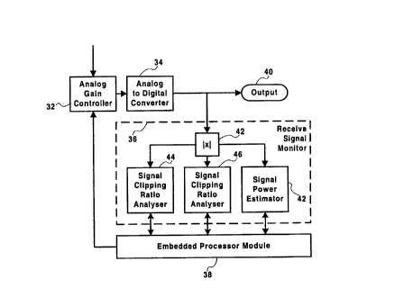
FIG. 5 shows the details of the received signal
monitor 36. A copy of the digital signal output by the
analog-to-digital converter 34 is rectified by a digital
rectifier 42. This operation consists of removing the
sign bit of the digital signal. Copies of the rectified
digital signal are processed by three components: a
command controllable signal power estimator 48 and two
command controllable signal clipping ratio analyzers 44
and 46. The signal power estimator 48 and signal
clipping ratio analyzers 44 and 46 operate under control
of the embedded processor module 38.
FIG. 6 shows the command controllable signal
clipping ratio analyzer 44 in more detail. A copy of the
rectified digital signal is first processed by a
comparator 50 and then passed to a leaky integrator 52.
- 12 -
CA 02308674 2000-OS-17
Both the comparator 50 and the leaky integrator 52
operate under control of the embedded processor
module 38. The leaky integrator outputs a computed
signal clipping ratio.
FIG. 7 shows the comparator 50 in more detail.
Comparator 50 has two modes of operation which can be
selected by sending an appropriate signal 56. In both
modes of operation, comparator 50 uses a threshold level
provided at a threshold level input 54 to perform its
function. The signal clipping ratio analyzer 46 receives
rectified digital samples from the digital signal
rectifier 42 at a rate at which the analog-to-digital
converter 34 outputs the samples. Each of the rectified
digital samples is compared to the threshold level
provided at input 54. According to the mode of operation
set by the input signal 56, the comparator 50 outputs
either 1 or the value of the rectified digital sample, if
the sample is less than the threshold. Otherwise, the
comparator 50 outputs a zero. The values output by the
comparator 50 are passed to the leaky integrator 52. The
operation of the leaky integrator 52 of the signal
clipping ratio analyzer 44 is similar to the operation of
the leaky integrator 60 of the signal power estimator 48
as described below.
The choice of the mode of operation is
dependent on the desired characteristics of the signal
clipping ratio analyzer 44. In the first mode, the
signal clipping ratio analyzer 44 computes the signal
clipping ratio and in the second mode, the signal
clipping ratio analyzer 44 computes the average amplitude
of the digitized samples which are above the threshold.
- 13 -
CA 02308674 2000-OS-17
FIG. 8 shows the implementation details of a
command controllable signal power estimator 48. The
signal power estimator 48 consists of a leaky
integrator 60. The leaky integrator 60 operates under
the control of an embedded processor module 38. The
leaky integrator 60 has two inputs: an input 62 provides
the leaky integrator with an initialization value and an
input 64 provides the leaky integrator with a convergence
time constant. The leaky integrator 60 performs a
mathematical function using the incoming rectified
digital samples. There is a set of mathematical
functions, well known in the art, which when applied to a
number of large consecutive sample values, outputs a
value that progressively converges to an average of these
values.
According to the preferred embodiment of the
invention, the leaky integrator 60 uses the following
averaging function:
LI out = (1-O)*previous output
+ O*latest received sample
wherein:
previous-output is LI out of the immediately
preceding sample period; and
0 < O < 1
The samples are received at the rate of the
analog-to-digital converter and the averaging function is
applied to the received samples at the same rate. The
convergence is dependent on the parameter O. Depending
on the choice of O, the output converges to the average
of the received samples in a short period of time or a
long period of time. When O is closer to zero, the
- 14 -
CA 02308674 2000-OS-17
averaging process implemented through the above-averaging
function is said to have a ~~long memory", converges
slowly to the average of the received samples and is very
resilient to variations in the value of the received
samples. Conversely, when O is close to one, the
averaging process has a ~~short memory", converges quickly
to the average of the received samples and is more
sensitive to variations in the value of the received
samples. Fast convergence as well as resilience to
variations in the value of the received samples are
required. A compromise is therefore made in choosing the
value of O to optimize both convergence time and
resilience to variations in the value of the received
samples. The value of O is empirically derived. The
output of the averaging function will invariably converge
to the average of the received samples. This will happen
regardless of an initial value of the output, but an
educated guess at what the initial value of the output
should speed up the convergence process.
According to the invention, a transceiver 20
disables data transmissions on start-up and, together
with the transmitter at the other end, enters a signal
gain adaptation process. The transmitter at the other
end generates a DMT signal 22. The receiver front-end of
the transceiver 20 receives the DMT signal 22, radio
frequency interference 26, as well as an echo signal 28
from the transmitter side of the transceiver. The
combined signal 24 is passed through an analog filter 30.
The analog filter 30 attenuates the echo signal 28 in
accordance with methods known in the art, and also
filters out the high radio frequency interferors in the
- 15 -
CA 02308674 2000-OS-17
AM band. The filtered signal is passed on to the analog
gain controller 32 which applies an initial amplification
factor to the analog DMT signal and then passes the
amplified signal to the analog-to-digital converter 34.
The analog-to-digital converter 34 outputs a digital copy
of the received DMT signal. For the gain adaptation
process, a copy of the digitized DMT signal is passed to
a command controllable received signal monitor 36.
In a first step of the adaptation, a rectified
copy of the digitized signal output by a digital signal
rectifier 42, is passed to a command controllable signal
power estimator 48. Under the control of an embedded
processor module 38, the command controllable signal
power estimator 48 is provided with an initial value 62
and a convergence time constant 64. The function of the
command controllable signal power estimator 48 is
implemented using a leaky integrator 60. The output of
the leaky integrator 60 represents the average signal
power of the received DMT signal subject to the
amplification performed by the analog gain controller 32.
The embedded processor module 38 analyzes the output of
the leaky integrator 60 and, when appropriate, sends a
command to the analog gain controller 32 to apply an
amplification factor to the received DMT signal. The
amplification is based on the output of the leaky
integrator weighted by an assumption of a worst case peak
to average ratio of the signal. Empirical evidence
indicates that an amplification factor of at least about
5 times the measured average power of the received signal
is appropriate.
- 16 -
CA 02308674 2000-OS-17
With the analog gain control adjusted for the
worst case, the received analog DMT signal is amplified
and passed to the analog-to-digital converter 34. A copy
of the digitized signal is passed through the digital
signal rectifier 42 to provide a rectified digitized
signal for two command controllable signal clipping ratio
analyzers 44, 46 and the signal power estimator 48. The
signal power estimator 48 again outputs an average signal
power value that is used to initialize the two signal
clipping ratio analyzers 44 and 46. The threshold of one
of the signal clipping ratio analyzers is set to an
initial value of about 1.5 to 2 times the average signal
power output by the signal power estimator 48. The
threshold of the other signal clipping ratio analyzer is
set to an initial value of about 2.2 to 2.8 times the
average signal power provided by the signal power
estimator 48. The leaky integrators of the command
controllable signal clipping ratio analyzers 44 and 46
are also provided with initial values and empirically
derived convergence time constants in a range of 2-8, to
2-2°. After a period in which enough data samples are
passed through the signal clipping ratio analyzers 44 and
46, the output values of the leaky integrators converge
to signal clipping ratios corresponding to the threshold
values set.
The embedded processor module 38 uses the two
signal clipping ratio analyzers plus a theoretical
clipping ratio corresponding to a threshold level of
zero, which results in a signal clipping ratio of 1.0, as
variables in a curve fitting algorithm employing a second
order function. The curve fitting algorithm enables the
- 17 -
CA 02308674 2000-OS-17
embedded processor module 38 to extrapolate a threshold
value corresponding to a target signal clipping ratio,
e.g., 10-'. Using an inverse of the extrapolated
threshold value and knowledge about the current
amplification factor of the analog gain controller 32, a
new amplification factor is calculated by the embedded
processor module 38. This new amplification factor is
sent to the analog gain controller 32, to permit the
analog gain controller 32 to adjust the amplitude of the
received analog DMT signal 22 contaminated by the RFI 26,
in order to utilize substantially all of a dynamic input
range of the analog-to-digital converter 34, thereby
minimizing quantization noise.
Table 2
Case One RFI Three rces
Source RFI
Sou
RFI to DMT
Power RatioIncreasedRFI ThresholdIncreasedRFI PAR Threshold
(dB) AGC gainPAR values AGC gain values
0 1.1 2.64 1.8,2.5 0.6 3.7 1.8,3
10 3.8 2.6_5 1.8,2.5 1.3 _3.45 1.8,3
4.5 2.3 1.4,2 1.8 3.34 1.8,3
5 2.57 1.4,2 2.1 ~ 3.38 1.8,3
~ ~
Table 2 shows a summary of analog gain control
increase achieved using the apparatus and method in
20 accordance with the invention. An improvement of up to a
5dB increase in analog gain control was achieved.
The results shown in Table 2 were obtained
during simulations of a) a single RFI source at 555KHz
and b) three RFI sources at 555KHz, 585KHz and 625KHz.
25 Each source was modulated with a random speech signal to
emulate real RFI. The DMT signal was adjusted to emulate
- 18 -
CA 02308674 2000-OS-17
a loop length of llkft with an echo path signal. The
power level of the DMT was measured at the input of the
ADC 34 (FIG. 4) and the RFI was normalized relative to
the DMT signal to simulate different RFI power scenarios.
As seen in Table 2, simulations were performed for RFI
power to DMT power at ratios of 0, 10, 20 and 30 dB.
As is apparent, the greatest increase in analog
gain control was achieved when the DMT was contaminated
by a single powerful RFI source, i.e., the analog input
to the AGC 32 was least Gaussian. The results shown in
Table 2 are indicative only of trends in performance
since the actual increases achieved in automatic gain
control are dependent on a plurality of factors discussed
above.
Although the invention has been described with
explicit reference to DMT transceivers, a person skilled
in the art will understand that the invention may be
applied to other forms of broadband transmission which
are susceptible to contamination from narrowband radio
frequency interference.
It should also be understood that the invention
may be practised using curve fitting algorithms of higher
orders, which would require a correspondingly larger
number of real-time measured signal clipping ratios.
Measurement of signal clipping ratios can be implemented
using a small number of command controllable signal
clipping analyzers by periodically changing the threshold
levels.
- 19 -