Note: Descriptions are shown in the official language in which they were submitted.
CA 02308683 2000-OS-17
Doc No. 10-149 CA Patent
MICRO-OPTIC DELAY ELEMENT FOR USE IN AN POLARIZATION
MULTIPLEXED SYSTEM
Field of the Invention
This invention relates generally to optical fiber communications and in
particular to
multiplexed communications that uses polarization multiplexing.
Background of the Invention
High-speed time-division-multiplexing (TDM) is a very attractive way of
enhancing the
spectrum efficiency of a large-capacity wavelength-division multiplexing (WDM)
system. One common architecture employs two modulators having a same bit rate,
wherein two separately modulated streams of data bits are combined into a high-
speed
single serial stream of data bits. Instead of providing a single higher-cost
higher-speed
modulator capable of providing modulation at a frequency of n Hz, two
modulators
having a frequency of n/2 Hz are provided and their outputs are time-
interleaved
providing a signal having a frequency of n Hz. However, one drawback to such a
scheme,
particularly in high-speed dense systems is that pulses from adjacent time
slots spread
2o and partially overlap one another and detection errors sometimes occur at a
receiver end.
One remedy for this is provided by an enhanced TDM system wherein adjacent
interleaved pulses are distinguishable as they are orthogonally polarized.
Such a scheme
is described in a paper entitled 1.04-Tbit/s SWDM Transmission Experiment
Based on
Alternate-Polarization 80-Gbit/s OTDM Signals, by Yutaka Miyamoto et al.,
published in
ECOC'98 20-24 September 1998 Madrid, Spain. In this paper alternate-
polarization
optical-TDM is described to increase the bit rate while keeping the signal
spectrum from
broadening. Here two modulated signals are time-division multiplexed with
additional
enhancement being achieved by polarization multiplexing of the two interleaved
TDM
streams.
CA 02308683 2000-OS-17
Doc No. 10-149 CA Patent
Another system using enhanced polarization optical TDM is described and
illustrated in
U.S. Patent No. 5,111,322 in the name of Bergano et al, entitled Polarization
Multiplexing Device with Solitons and Method Using Same, incorporated herein
by
reference. In this patent, a transmission system's capacity is increased by
using a
combination of polarization and time-division multiplexing. More specifically,
two
streams of differently (preferably orthogonally) polarized solitons are
interleaved (time-
division-multiplexed) at a transmitter, and later separated at the receiver to
recover both
data streams.
to The multiplexing of 2 channels of 2.5 Gbits/s each, into a single 5 Gbits/s
channel, and
the corresponding demultiplexing at the receiving end, is described in
conjunction with
the multiplexor of FIG. 2 in prior art US patent 5,111,322.
In FIG. 2 the signal source for the two channels is a single, mode-locked
laser 201,
15 producing about 35-50 ps wide soliton pulses at a 2.5 GHz rate. Its output
is split into two
soliton pulse streams having essentially orthogonal polarizations, in a
sputter 202, and
each half separately modulated (with different information bearing signals
labeled Data 1
and Data 2) in modulators 205 and 206. Modulator 205 receives a first
information
bearing signal or data stream on line 207, while modulator 206 receives a
second data
20 stream on line 208. The two soliton pulse streams then recombine in a
sputter 210, but
only after one of the pulse streams is delayed by one-half of the 2.5 Gbit/s
bit period in an
adjustable delay line 209 so that the two pulse streams are interleaved in
time.
A few practical details concerning the apparatus of FIG. 2 are in order here.
25 The modulators 205, 206 should preferably be of the LiNbO3, balanced
Mach-Zehnder type, as those produce virtually no chirping of the soliton
pulses,
and have an adequate on-off ratio (.about.20 dB). The required linear
polarizations at the
inputs to modulators 205, 206, and for the polarization multiplexing itself,
can either be
maintained through the use of (linear) polarization-preserving fiber
throughout the
3o multiplexor, or through the use of polarization controllers, such as
controllers 211-214,
both before and after modulators 205, 206 as shown in FIG. 2. Polarization
controllers
CA 02308683 2000-OS-17
Doc No. 10-149 CA Patent
211-214 may be arranged as described in an article by H. C. Levevre, "Single-
Mode
Fiber Fractional Wave Devices and Polarization Controllers", Electronics
Letters, Vol.
16, p. 778, 1980. For the temporal interleaving of the two soliton pulse
streams, it is
necessary to make precise adjustment of the relative lengths of the two arms
of the
multiplexor. This can be done with adjustable delay line 209 which is shown
interposed
between the output of modulator 206 and polarization sputter 210.
Nevertheless, delay
line 209 is not absolutely necessary. It is also possible to trim the length
of one or the
other arm, through one or two trials, to within a few picoseconds of the
correct length so
the apparatus may remain all-waveguide throughout.
The original soliton pulse stream output from the correctly adjusted
multiplexer of FIG. 2
would appear as shown in FIG. 3. The x and y axes represent intensities of
pulses of
different (orthogonal) polarizations. As an example, soliton pulses 301 and
302 have an
initial polarization along the axis and a period of 400 ps. Soliton pulses 303
and 304 have
an orthogonal (y direction) polarization, the same period, and are time
interleaved with
the first series of pulses. Information is carried in the pulse streams by
virtue of the
presence or absence of pulses at the expected or nominal positions on the time
axis. Note
that launching the soliton pulses as in FIG. 3 not only achieves the potential
for combined
time and polarization division demultiplexing at the receiving end, but also
virtually
2o eliminates the potential for cross-phase modulation, and hence virtually
eliminates the
potential for interaction during transmission, between the two channels.
An alternative circuit to Fig. 2 is shown in Fig. 1, wherein two laser sources
are shown,
oriented to provide two orthogonally polarized beams; in all other respects,
the circuit of
Fig. 1 functions in a similar manner to the circuit of Fig. 2, however is
absent the
polarization controllers,211 and 212.
The aforementioned prior art reference by Miyamoto et al. teaches the use of
delay lines
to time-skew the pulse trains that are to be multiplexed. For example, the
paper discloses
3o using two different lengths of polarization maintaining fibre in order to
create a suitable
delay. Although using different lengths of optical fibre provides a necessary
delay,
CA 02308683 2000-OS-17
Doc No. l0-149 CA Patent
ensuring that this delicately balanced network is stable over a range of
temperatures is not
trivial.
Althhough the prior art optical circuits to some degree provide solutions for
polarization
time-division multiplexing, the '322 patent for example describes a rather
complex
optical circuit where polarization controllers are shown to control the
polarization state of
the light propagating through the optical fibres.
In contrast, the circuit in accordance with this invention is a micro-optic
circuit that does
not rely on the use of polarization controllers and does not require
polarization-
maintaining optical fibre.
Furthermore, an aspect of the instant invention provides a micro-optic delay
element,
which utilizes the polarization difference between two data-streams to be time-
i s multiplexed while preserving the polarization state of the two orthogonal
streams.
Furthermore, the instant invention provides a solution, which is considerably,
more
temperature-stable than using two separate waveguides and independently
controlling for
any temperature difference between the two waveguides.
2o Summary of the Invention
In accordance with the invention a circuit is provided for receiving two
streams of data
and for polarization time-division multiplexing the two streams of data onto a
single
waveguide such that one of the data streams is delayed by a time td from the
other data
25 stream, comprising:
a first modulator having an input port and an output port for modulating input
light and
for providing a first modulated data stream;
a second modulator having an input port and an output port for modulating
input light
and for providing a second modulated data stream;
3o a first lens for collimating light provided by the first modulator;
a second lens for collimating light provided by second modulator,
CA 02308683 2000-OS-17
Doc No. 10-149 CA Patent
the first and second lenses each for providing a substantially collimated
substantially unguided beam of light to at least another component;
a polarization beam splitter/combiner having two input ports at one end
optically coupled
to receive the substantially collimated, substantially unguided beams of
light, said
polarization beam splitter/combiner having a combining port at another end for
combining the data streams such that one data stream delayed by a time td from
the other
data stream,
light traversing parallel paths from the first and second lenses respectively
to the
polarization beam splitter combiner being substantially unguided, so that
light traversing
1 o at least one of said parallel paths will have a polarization state which
is substantially
unchanged.
In accordance with the invention, there is provided a circuit for receiving
two streams of
modulated data and for polarization and time-division multiplexing the two
streams onto
a single waveguide, comprising:
a polarization rotator for rotating the polarization of one of the two
modulated data
streams; and,
a birefringent crystal having at least two input ports disposed at one end to
receive the
two modulated data streams having orthogonal polarization states, the
birefringent crystal
2o having an output port disposed at an opposite end to receive and combine
the two
modulated data streams into a single time-interleaved data stream, the
birefringent
crystal being of suitable length for providing a path length difference
between each of
the at least two input ports and the output port to provide a required time
delay at the
output port between the two data streams.
In accordance with the invention, there is provided a circuit for receiving
two streams of
modulated data and for polarization and time-division multiplexing the two
streams onto
a single waveguide, comprising:
a light source for providing a primary signal;
3o a first and a second modulator for independently, and in parallel
modulating the primary
signal, the first and second modulators for providing two data streams ;
CA 02308683 2000-OS-17
Doc No. l0-149 CA Patent
means for operating on at least one of the two data streams relatively
orthogonalizing the
two data streams; and, ,
a birefringent crystal having at least two input ports at an end thereof
disposed to receive
the two modulated data streams having orthogonal polarization states, the
birefringent
crystal having an output port disposed at an opposite end thereof to receive
and combine
the two modulated data streams into a single time-interleaved data stream, the
birefringent crystal being of suitable length for providing a path length
difference
between each of the at least two input ports and the output port to provide a
required
time delay at the output port between the two data streams.
In accordance with another aspect of the invention, a method of multiplexing
optical
signals onto an output port is provided. The method comprises the steps of:
providing two modulated polarized optical signals having a polarization
difference
between the two modulated signals of substantially 90 degrees;
passing one of the two modulated signals along a first path in a birefringent
crystal;
passing another of the two modulated signals along a second path intersecting
the first
path at the output port of the birefringent crystal.
In accordance with the invention there is provided a fibreless optical circuit
for receiving
2o two streams of modulated data and for polarization multiplexing the two
data streams
onto a single waveguide, comprising:
a modulator module for independently, and in parallel, modulating optical
signals and for
providing two data streams;
a birefringent crystal having at least two input ports at an end thereof
disposed to receive
the two modulated data streams having different polarization states, the
birefringent
crystal having an output port disposed at an opposite end thereof to receive
and combine
the two modulated data streams into a single multiplexed data stream, the
birefringent
crystal being of suitable dimensions to provide time division polarization
multiplexing,
the circuit being fibreless such that there is an absence of optical fibre
between the
modulator module and the birefringent crystal for coupling light therebetween.
CA 02308683 2000-OS-17
Doc No. 10-149 CA Patent
Conveniently, if a delay is required that exceeds the delay that is provided
by traversing
the first and second paths of the birefringent crystal having different
optical lengths, a
spacer can be inserted into each of the signal paths prior to the signals
reaching the
birefringent crystal, wherein the spacers are of a substantially different
refractive index.
This method is quite suitable when optically coupling a lithium niobate
modulating block
with a ruble crystal, wherein no optical fibres are used except perhaps
coupled to output
ports.
In summary, the devices in accordance with this invention are small and
compact and
integrated. Yet still further, due to their compactness are somewhat easier to
temperature
control than, for example the prior art circuits shown. Yet still further, and
perhaps more
importantly, the optical circuit including the modulator focusing optics
between the
modulator and a polarization beam splitter/combiner do not require any optical
fibre for
coupling of light therebetween. Advantageously, by an providing a relatively
unguided
light path, polarization controllers or polarization maintaining fibre is not
required. As
well by providing block like elements coupled to one another, i.e. one or more
modulator
blocks coupled to rod GRIN lenses, coupled to a birefringent crystal yields a
compact
easy to assemble device that can be conveniently packaged.
Brief Description of the Invention
Exemplary embodiments of the invention will now be described in conjunction
with the
drawings in which:
FIG. 1 is a prior art schematic diagram of a multiplexing circuit using 2
laser light
sources oriented to yield orthogonal polarized light;
FIG. 2 illustrates a prior art schematic of a multiplexing circuit;
FIG. 3 illustrates the pulse field envelopes at the output of the multiplexor
of FIG. 2;
3o FIG. 4 illustrates a schematic circuit block diagram of an enhanced TDM
multiplexor in
accordance with this invention;
CA 02308683 2000-OS-17
Doc No. 10-149 CA Patent
FIG. 5 is a schematic block diagram which illustrates a portion of the circuit
used for
multiplexing and which illustrates the operation of that circuit portion;
Fig. 6 is a more detailed embodiment illustrating the circuit of Fig. 5;
Fig. 7 is an alternative embodiment to the circuit of Fig. 6, wherein two
spacers having
different refractive indices are utilized to achieve a time delay between
signals traversing
the two spacers;
Fig. 8 is a schematic block diagram of a preferred embodiment of the invention
showing
the modulator module coupled to a ruble crystal via a pair of substantially
quarter pitch
1 o collimating GRIN lenses; and,
Fig. 9 is a schematic block diagram illustrating a polarization beam
splitter/combiner in
the form of a polarization beam splitting cube.
Detailed Description
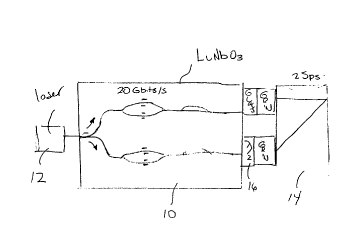
Turning now to FIG. 4, a substantially integrated micro-optic circuit is shown
having a
slab waveguide chip 10 having an end optically coupled with a laser 12 and
having an
end optically coupled with a birefringent crystal 14. At an input end of the
crystal 14, a
half waveplate 16 is provided for rotating the polarization of the light
passing
2o therethrough by 90°.
The slab waveguide chip is LiNb03 having waveguide disposed therein. The
waveguides
can be formed by ion implantation or alternatively by grafting polymer or
other such light
transmissive material into the chip. Electrical contacts are disposed about
the waveguides
1 Sa, 1 Sb, 15c... and in operation a voltage is be applied to modulate the
signal passing
between the contacts. Variable attenuators are provided at the output for
controlling the
amplitude of the modulated signals. Although LiNb03 is a preferred modulator,
of course
other types of modulators my be used, for example electro-absorption or GaAs.
Aside
from the compactness and temperature stability of the circuitry shown within
the
3o waveguide 10, the operation and interconnection of the components is
substantially
similar to the circuitry shown if FIG. 2. Notwithstanding, one major
difference between
8
CA 02308683 2000-OS-17
Doc No. 10-149 CA Patent
the circuit of the instant invention, shown in FIG. 4 and the prior art
circuits, is the
provision of the birefringent crystal for use as a polarization combiner and
delay line for
time-division polarization interleaving of pulses. One even more significant
difference in
this circuit and prior art circuits for time-division polarization
multiplexing is the
fibreless nature of the circuit from the modulator module 10 to the beam
splitter/combiner, for example shown here in the form of a crystal 14. By
coupling
substantially collimating lenses, for example, quarter pitch GRIN lenses to
the modulator
10, collimated beams are provided to next elements in sequence and to the
crystal 14.
Since the substantially collimated beam traverses the glass spacer and quarter
waveplate
1 o substantially unguided, its polarization state is substantially unaltered.
Fig. 5 illustrates a portion of the circuit shown in Fig. 4 depicting the
operation of the
polarization combining and multiplexing circuit. This circuit conveniently
provides the
added advantage of achieving a predetermined required delay. A stream of
pulses spaced
by 25 ps are provided at the input end of each of the GRIN lenses SOa. Light
directed
through the bottom GRIN lens is rotated by 90 degrees by the waveplate 16. As
can be
seen in figure, this beam must travel a greater distance to reach GRIN lens
SOb, than the
beam that follows a straight through path launched into the upper GRIN lens
SOa. This in
effect skews the pulses in time that were launched simultaneously into the two
GRIN
lenses such that the orthogonally polarized pulses become combined and time
multiplexed, as shown at the output of the GRIN lens SOb. Fig. 6 (not drawn to
scale)
illustrates in more detail, dimensions of a birefringent or ruble crystal that
achieves a
desired time delay to provide time multiplexing of these two orthogonally
polarized
streams of pulses. The length of the crystal in this exemplary embodiment is
27 mm, and
the with is 5 mm. Of course to some extent, the size of a crystal that is
required is
proportional to it cost. Fig. 7 illustrates yet another embodiment, wherein a
spacer of
glass 17 is inserted into the upper optical path, and a spacer of silicone 18
provides a
portion of the lower optical path. By selecting light transmissive materials
such as glass
and silicone that have a substantially different refractive indexes in the two
paths the
3o beams must follow, delays in addition to delay provided by the birefringent
crystal 14 can
be enhanced and further controlled between the two. For example, in Fig. 7,
the silicone
CA 02308683 2000-OS-17
Doc No. 10-149 CA Patent
spacer 18 shown, has a much higher refractive index than the glass spacer 17;
light
traveling through the silicone propagates therethrough slower than light
traveling through
a similar length of glass. Notwithstanding, a birefringent crystal of at least
some
minimum proportions is required. In the example shown, the beams propagating
through
the birefringent crystal 14 are collimated or near-collimated and
substantially separated
at the input end of the ruble. Thus, the crystal must be of dimensions that
will support
two beams, combine them, and provide a suitable required delay even in the
instance that
additional delay is provided by the silicone spacer. However, it can be seen,
by
comparing Figs. 6 and 7, that the overall dimensions of the rutile, required
to combine
1 o and time multplex the two pulse streams is substantially lessened in the
embodiment of
Fig. 7. Nevertheless, this embodiment requires suitable antireflection coating
between the
GRIN lens SOa and the silicone spacer.
Numerous other embodiments can be envisaged without departing from the
invention, for
1 s example, the polarization beam splitter/combiner described heretofore, is
a ruble crystal,
however, a polarization beam splitting cube could be used instead of the ruble
as is
shown in Fig. 9
In embodiments described heretofore, a half wave plate is shown for rotating
the
2o polarization along one path, however, it is conceivable to provide
orthogonally polarized
beams of light to the modulator, obviating the requirement of a rotator.
10