Note: Descriptions are shown in the official language in which they were submitted.
CA 02309232 2000-OS-24
_ 1 _
MICRO-ELECTROMECHANICAL DEVICE, LIQUID DISCHARGE HEAD,
AND METHOD OF MANUFACTURE THEREFOR
BACKGROUND OF THE INVENTION
Field of the Invention
The present invention relates to a micro-
electromechanical device, a liquid discharge head, and
a method of manufacture therefor.
Related Background Art
The liquid discharge head, which is one example of
the micro-electromechanical device used conventionally
for an ink jet printer or the like, is such that liquid
in each of the flow paths is heated and bubbled by_
means of heating elements, respectively, and that.
liquid is discharged from each of the discharge ports
by the application of pressure exerted when liquid is
bubbled. Each of the heating elements is arranged on
an elemental substrate, and driving voltage is supplied
to each of them through wiring on the elemental
substrate.
For a liquid discharge head of the kind, there is
a structure in which a movable member is arranged in
the flow path in a cantilever fashion where one end of
the movable member is supported. One end (fixedly
supported portion) of this movable member is fixed onto
the elemental substrate, while the other end (movable
portion) is made extendable into the interior of each
CA 02309232 2000-OS-24
- 2 -
liquid flow path. In this manner, each movable member
is supported on the elemental substrate with a certain
gap with the surface thereof, and arranged to be
displaceable in each flow path by the pressure exerted
by bubbling or the like.
For the conventional example described above, the
wiring is formed on the elemental substrate. The
wiring is extremely thin, and its resistance value is
great. Then, from this elemental substrate, the wiring
is connected with the external driving circuit or the
like. However, with such large resistance value of the
wiring, the electrical loss becomes great inevitably.
Also, in order to make the resistance value smaller
even by a slight amount, the wiring should preferably
be made flat and wide. As a result, the liquid
discharge head is formed in a larger size inevitably.
SUMMARY OF THE INVENTION
Now, therefore, the present invention is designed
with a view to solving the problems discussed above.
It is an object of the invention to provide a micro-
electromechanical device capable of reducing the
electrical loss of wiring without making the structure
complicated or making the size of the device large. It
is also the object of the invention to provide a liquid
discharge head and a method of manufacture therefor.
In order to achieve the object of the invention
CA 02309232 2000-OS-24
- 3 -
discussed above, it has a feature given below.
The micro-electromechanical device of the present
invention comprises a fixedly supporting portion and a
movable portion, and a substrate for supporting the
movable member which is supported in a state having a
specific gap with the substrate. For this device,
a metallic layer which provides the gap for the movable
portion is covered by the fixedly supporting portion of
the movable member, and remains to be used as a wiring
layer.
Also, the wiring layer is electrically connected
with a plurality of wirings provided for the substrate.
Another feature of the present invention is the
provision of a liquid discharge head comprising an
elemental substrate; a ceiling plate laminated on the
elemental substrate; a flow path formed between the
elemental substrate and the ceiling plate; and a
movable member each having a fixedly supporting portion
and a movable portion, the movable portion of which is
positioned in each of the flow paths. Here, the
movable member is supported in a state having a
specific gap with the elemental substrate. For this
liquid discharge head, a metallic layer for providing
the gap for the movable portion is covered by the
fixedly supporting portion of the movable member, and
remains to be used as a wiring layer.
Also, this liquid discharge head, a heating
CA 02309232 2000-OS-24
- 4 -
element is provided for the elemental substrate
corresponding to the flow path, and the aforesaid
wiring layer may be electrically connected with the
heating element through wiring.
With the structure thus arranged, at least a part
of the metallic layer that forms a sufficiently thick
gap can be utilized as wiring, hence making it possible
to reduce the value of electric resistance.
Also, a method of the present invention for
manufacturing a liquid discharge head, which is
provided with an elemental substrate, a ceiling plate
laminated on the elemental substrate, and a flow path
formed between the elemental substrate and the ceiling
plate, comprises the steps of forming a metallic layer
for the formation of a gap on the elemental substrate;
forming a thin film layer on the metallic layer to
become a movable member; removing a portion of-the
metallic layer positioned below the movable portion of
the movable member, while keeping the portion of the
movable member positioned below the fixedly supporting
portion to remain intact; and making at least a part of
the remaining portion of the metallic layer as a wiring
layer to be electrically connected with the wiring
pattern on the elemental substrate.
Here, the thin film layer is formed by SiN, and
the metallic layer is formed by A1 or may be formed by
A1 alloy.
CA 02309232 2000-OS-24
- 5 -
In this respect, the term "upstream" and the term
"downstream" referred to in the description hereof are
used to express the flow direction of liquid from the
liquid supply source toward the discharge ports through
the bubbling areas (or movable members) or to express
the structural directions.
BRIEF DESCRIPTION OF THE DRAWINGS
Fig. 1 is a cross-sectional view which illustrates
the structure of a liquid discharge head in accordance
with one embodiment of the present invention, taken in
the liquid flow direction.
Fig. 2 is a cross-sectional view which shows the
elemental substrate used for the liquid discharge head
represented in Fig. 1.
Fig. 3 is a cross-sectional view which illustrates
the electrical connection of the liquid-discharge head
represented in Fig. 1, taken in the liquid flow path.
Fig. 4 is a plan view which schematically shows
the liquid discharge head represented in Fig. 3 without
the protection layer and others.
Fig. 5 is a schematically sectional view which
shows the elemental substrate by vertically sectioning
the principal elements of the elemental substrate
represented in Fig. 2.
Figs. 6A, 6B, 6C, 6D and 6E are views which
illustrate a method for forming a movable member on an
CA 02309232 2000-OS-24
- 6 -
elemental substrate.
Fig. 7 is a view which illustrate a method for
forming SiN film on the elemental substrate by use of a
plasma CVD apparatus.
Fig. 8 is a view which illustrate a method for
forming SiN film on the elemental substrate by use of a
dry etching apparatus.
Figs. 9A, 9B and 9C are views which illustrate a
method for forming movable members and flow path side
walls on an elemental substrate.
Figs. 10A, lOB and lOC are views which illustrate
a method for forming movable members and flow path side
walls on an elemental substrate.
Fig. 11 is a plan view which schematically shows
the wiring area on the elemental element of the liquid
discharge head in accordance with the first embodiment
of the present invention.-- -----
Fig. 12 is a cross-sectional view which
illustrates the electric connection of the liquid
discharge head in accordance with a third embodiment of
the present invention, taken in the flow path
direction.
Fig. 13 is a schematic view of a circuit which
illustrates the electrical connection of the liquid
discharge head in accordance with the first embodiment
of the present invention.
Fig. 14 is a schematic view of a circuit which
CA 02309232 2000-OS-24
_ 7 _
illustrates the electrical connection of the liquid
discharge head in accordance with the third embodiment
of the present invention.
DETAILED DESCRIPTION OF THE PREFERRED EMBODIMENTS
Now, the description will be made of a liquid
discharge head as one embodiment to which the present
invention is applicable, which comprises a plurality of
discharge ports for discharging liquid; a first
substrate and a second substrate, which are bonded
together to form a plurality of liquid flow paths
communicated with each of the discharge ports; a
plurality of energy converting elements arranged in
each of the liquid flow paths for converting electric
energy to energy for discharging liquid in each liquid
flow path; and a plurality of elements having different
functions or electric circuits for controlling the
driving condition of each of the energy converting
elements.
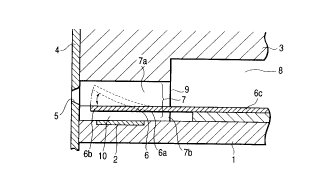
Fig. 1 is a cross-sectional view which shows the
leading end portion of a liquid discharge head
schematically in accordance with one embodiment of the
present invention, taken in the liquid flow direction.
As shown in Fig. 1, the liquid discharge head is
provided with the elemental substrate 1 having the
plural numbers (in Fig. 1, only one is shown) of
heating elements 2 arranged in parallel lines, which
CA 02309232 2000-OS-24
_ g _
generate thermal energy for creating bubbles in liquid;
the ceiling plate 3 which is bonded to the elemental
substrate 1; the orifice plate 4 bonded to the front
faces of the elemental substrate 1 and ceiling plate 3;
and movable member 6 installed in the liquid flow paths
7 formed by the elemental substrate 1 and the ceiling
plate 3.
The elemental substrate 1 is the one having a
silicon oxide or silicon nitride film formed on the
substrate of silicon or the like for insulation and
heat accumulation, and also, having thereon the
electric resistive layer and wiring formed by
patterning, thus making each of the heating elements 2.
Each of the heating elements 2 generates heat when
voltage is applied from the wiring to the electric
resistive layer to enable electric current to run on
it.
The ceiling plate 3 is the one that forms a
plurality of liquid flow paths 7 corresponding to each
of the heating elements 2, and a common liquid chamber
8 for supplying liquid to each of the liquid flow paths
7. The ceiling plate 3 is integrally formed with the
liquid path side walls 9 that extend between each of
the heating elements 2 from the ceiling portion. The
ceiling plate is formed by silicon material to be able
to provide the patterns of the liquid flow paths 7 and
the common liquid chamber 9 by means of etching, or to
CA 02309232 2000-OS-24
_ g _
form the liquid flow path 7 portion by means of etching
after depositing the material that becomes the liquid
flow path side walls 9, such as silicon nitride,
silicon oxide, on the silicon substrate by the known
film formation method of CVD or the like.
For the orifice plate 4, a plurality of discharge
ports 5 are formed corresponding to each of the liquid
flow paths 7, and communicated respectively with the
common liquid chamber 8 through the liquid flow paths
7. The orifice plate 4 is also formed by silicon
material. For example, this plate may be formed by
cutting the silicon substrate used for forming the
discharge ports 5 to a thickness of approximately 10 -
150 um. In this respect, the orifice plate 4 is not
necessarily among the constituents of the present
invention. Instead of the provision of the orifice
plate 4, it may be possible to make a ceiling plate
with discharge ports 5 by processing the front end face
of the ceiling plate 3 to leave a wall intact in a
thickness equivalent to that of the orifice plate 4
when the liquid flow paths 7 are formed on the ceiling
plate 3.
The movable member 6 is a thin film in the form of
a cantilever which is arranged to face the heating
element 2 and divide the first liquid flow path 7a
communicated with the discharge port 5 of the liquid
flow path 7 into the second liquid flow path 7b. Each
CA 02309232 2000-OS-24
- 10 -
of the movable members is formed by a silicon
insulation material, such as silicon nitride, silicon
oxide.
The movable member 6 is arranged in a position to
face the heating element 2 with a specific distance
from the heating element 2 in a state to cover the
heating element 2 so that the fixedly supporting
portion 6c is provided for this member on the upstream
side of a large flow which runs by the discharge
operation of liquid from the common liquid chamber 8 to
the discharge port 5 side through the movable member 6,
and that the movable portion 6b is provided for this
member on the downstream side with respect to the
fixedly supporting portion 6c. The gap between the
heating element 2 and the movable member 6 becomes each
of the bubbling areas 10.
Now, when the heating -element 2 --i-s driven -to give
heat in accordance with the structure described above,
heat is applied to liquid on the bubbling area 10
between the movable member 6 and the heating element 2.
Then, on the heating element 2, bubbles are generated
and developed by film boiling phenomenon. The pressure
exerted by the development of each bubble acts upon the
movable member 6 priorly to enable the movable member 6
to be displaced to open widely to the discharge port 5
side centering on the fulcrum 6a as indicated by broken
line in Fig. 1. Due to the displacement of the movable
CA 02309232 2000-OS-24
- 11 -
member 6 or due to being in the displaced state of the
movable member, the propagation of the pressure and the
development of the bubble itself brought about by the
generation of the bubble are led to the discharge port
5 side, hence discharging liquid from the discharge
port 5.
In other words, with the movable member 6 provided
for the bubbling area 10, having the fulcrum 6a on the
upstream side (common liquid chamber 8 side) of the
liquid flow in the liquid flow path 7, and the movable
portion 6b on the downstream side (discharge port 5
side) thereof, the direction of the bubble pressure
propagation is led to the downstream side, thus
enabling the bubble pressure to directly contribute to
the effective performance of discharge. Then, the
direction of the bubble development itself is also led
to the downstream side in the same way as the direction
of the pressure propagation to make it to be developed
larger in the downstream side than the upstream side.
Now that the direction of the bubble development itself
is controlled by the movable member, and also, the
direction of the bubble pressure propagation is
controlled as described above, it becomes possible to
improve the fundamental discharge characteristics, such
as the discharge efficiency and discharge power or the
discharge speeds, among some others.
Meanwhile, when the bubble enters the defaming
CA 02309232 2000-OS-24
- 12 -
process, the bubble is defamed rapidly. Then, the
movable member 6 returns lastly to the initial position
indicated by solid line in Fig. 1. At this juncture,
liquid is allowed to flow in from the upstream side,
that is, the common liquid chamber 8 side in order to
make up the contracted volume of bubble on the bubbling
area 10 or to make up the voluminal portion of liquid
that has been discharged. Here, the liquid refilling
is made in the liquid flow path 7, but this liquid
refilling is performed efficiently, rationally, and
stably along with the returning action of the movable
member 6.
Also, the liquid discharge head of the present
embodiment is provided with the circuits and elements
for driving each of the heating elements 2, and also,
for controlling the driving thereof. These circuits
and elements are arranged on the elemental substrate 1
or on the ceiling plate 3 depending on each of the
functions that should be carried out by them as
allocated accordingly. Also, these circuits and
elements can be formed easily and precisely by the
application of the semiconductor wafer processing
technologies, because the elemental substrate 1 and the
ceiling plate 3 are structured by use of silicon
material.
Hereunder, the description will be made of the
structure of the elemental substrate 1 formed by the
CA 02309232 2000-OS-24
- 13 -
application of the semiconductor wafer processing
technologies.
Fig. 2 is a cross-sectional view which shows the
circumference of a heating element os the elemental
substrate used for the liquid discharge head
represented in Fig. 1. As shown in Fig. 2, the
elemental substrate 1 used for the liquid discharge
head of the present embodiment is formed by laminating
the thermal oxidation film (Si02 layer in a thicl~ness of
approximately 0.55 um, for example) 302 and the
interlayer film 303 that dually functions as the heat
accumulation layer on the surface of the substrate 301
formed by silicon (or ceramics) in that order. As the
interlayer film 303, SiOz film or Si3N4 film is used.
On the surface of the interlayer film 303, a resistive
layer (TaN layer in a thickness of approximately 1000
~1, for example) 304 is partly formed. Then, on the
surface of the resistive layer 304, the wiring 305 is
partly formed. As the wiring 305, A1 wiring or A1
alloy wiring, such as A1 - Si, A1 - Cu, in a thickness
of approximately 5000 ~ is used. The wiring 305 is
patterned by the photolithographic method and wet
etching method. The resistive layer 304 is patterned
by the photolithographic method and dry etching method.
On the surface of the wiring 305, resistive layer 304,
and interlayer film 303, the protection layer 306 is
formed by Si02 or Si3N4 in a thickness of approximately
CA 02309232 2000-OS-24
- 14 -
1 um. On the portion and the circumference thereof of
the surface of the protection film 306, which
correspond to the resistive layer 304, the cavitation
proof film (SiN layer in a thickness of approximately
2000 ~, for example) 307 is formed in order to protect
the protection film 306 from the chemical and physical
shocks following the heating of the resistive layer
304. The surface of the resistive layer 304, where the
wiring 305 is not formed, becomes the thermoactive
portion (heating element) 308 where the heat of the
resistive layer 304 is activated.
The films on the elemental substrate 1 are formed
one after another on the surface of the silicon
substrate 301 by the application of the semiconductor
manufacturing technologies and techniques. Thus, the
thermoactive portion 308 is provided for the silicon
substrate 301. -- - -- -
Fig. 3 is a cross-sectional view which shows in
detail the circumference of the fixedly supporting
portion of the movable member of the elemental
substrate. Fig. 4 is a schematic plan view thereof.
As described earlier, the heat accumulation layer 302
and the interlayer film 303 are laminated on the
substrate 301. Then, the resistive layer 304 and the
wiring 305 are patterned, respectively. Also, in the
gap between the interlayer film 303 and the resistive
layer 304, the wiring 210 is partly formed. Further,
CA 02309232 2000-OS-24
- 15 -
The protection film 306 and the cavitation proof film
307 are laminated. Then, on the part of the interlayer
film 303, the through hole 211 is formed. Also, for
the protection film 306, the through hole 201 is formed
by means of the dry etching or the like.
Then, by use of the sputtering method, there are
formed the metallic layer (A1 layer in a thickness of
approximately 5 um, for example) 71 for the formation
of the gap, and the protection layer (TiW layer in a
thickness of approximately 3000 ~1, for example) 202
(see Fig. 11). The thickness of the metallic layer 71
that forms this gap becomes the gap dimension between
the movable member 6 and the resistive layer 304 which
serves as the base thereof.
With the structure thus arranged, the wiring 305
is electrically connected with the wiring 210 by way of
the through hole 211 and the resistive layer 304.
Further, the metallic layer 71 that forms the gaps is
electrically connected with the wiring 305 by way of
the through hole 201 and the resistive layer 304.
Continuously, then, the SiN thin film layer 72
that becomes the movable member 6 is laminated by the
CVD method for its formation in a thickness of 5 um.
Further, after that, by the photolithographic method
and dry etching method, the SiN thin film layer 72 is
patterned to form the movable member 6 having the
movable portion 6b and the fixedly supporting portion
CA 02309232 2000-OS-24
- 16 -
6c thereof. At the same time, in accordance with the
present invention, the metallic layer 71 that forms the
gap should be used as the wiring. Therefore, a part of
the Sin thin film layer 72 that becomes the movable
member 6 is left intact on a specific location on the
surface of the metallic layer 71 for the purpose to
enable such part to function as the protection film for
the wiring thus arranged.
Then, by means of the wet etching, the portion of
the metallic layer 71 that forms the gap, which is
positioned below the movable portion 6b of the movable
member 6 (that is, the remaining portion of the thin
film layer 72) is removed together with the other
unwanted portions. Thus, it is arranged to leave
intact the portion of the metallic layer 71 that forms
the gap, which is positioned below the fixedly
supporting portion 6c of the movable portion 6b (that
is, the remaining portion of the thin film layer 72).
This portion is designated as the metallic layer 71a
that forms the gap. In this way, the movable member 6
is formed with the one end being in the cantilever
fashion in which the fixedly supported portion of the
movable member is fixed on the metallic layer 71a that
forms the gap. Lastly, the protection layer 202 formed
by TiW (see Fig. 11) is removed by etching the entire
surface of the HZO2. Then, using the photographic
method the electrode pad portion is patterned to
CA 02309232 2000-OS-24
- 1~ -
compete the elemental substrate.
Here, by the utilization of the metallic layer 71a
that forms the gap as the wiring layer, it becomes
possible to reduce the resistance value of the wiring
approximately by 1/2 to 1/5 times in total, because the
thickness of this layer is made approximately 5 to 10
times the thickness of the conventional one.
Fig. 5 is a schematically cross-sectional view
which shows the elemental substrate 1 by vertically
sectioning the principal elements of the elemental
substrate 1 represented in Fig. 2.
As shown in Fig. 5, the N type well region 422 and
the P type well region 423 are Socally provided for the
surface layer of the silicon substrate 301 which is the
P conductor. Then, using the general MOS process the
P-MOS 420 is provided for the N type well region 422,
and the N-MOS 421 is provided for the P type--well
region 423 by the execution of impurity plantation and
diffusion, such as the ion plantation. The P-MOS 420
comprises the source region 425 and the drain region
426, which are formed by implanting the N type or P
type impurities locally on the surface layer of the N
type well region 422, and the gate wiring 435 deposited
on the surface of the N type well region 422 with the
exception of the source region 425 and the drain region
426 through the gate insulation film 428 which is
formed in a thickness of several hundreds of ~, and
CA 02309232 2000-OS-24
- 18 -
some others. Also, the N-MOS 421 comprises the source
region 425 and the drain region 426, which are formed
by implanting the N type or P type impurities locally
on the surface layer of the P type well region 423, and
the gate wiring 435 deposited on the surface of the P
type well region 423 with the exception of the source
region 425 and the drain region 426 through the gate
insulation film 428 which is formed in a thickness of
several hundreds of ~, and some others. The gate
wiring 435 is made by polysilicon deposited by the CVD
method in a thickness of 4000 ~ - 5000 ~. Then, the C-
MOS logic is structured with the P-MOS 420 and the N-
MOS 421 thus formed.
The portion of the P type well°region-423, which m
is different from that of the N-MOS 421, is provided
with the N-MOS transistor 430 for driving use of the
electrothermal converting element. 'rhe N-MOS
transistor 430 also comprises the source region 432 and
the drain region 431, which are provided locally on the
surface layer of the P type well region 423 by the
impurity implantation and diffusion process or the
like, and the gate wiring 433 deposited on the surface
portion of the P type well region 423 with the
exception of the source region 432 and the drain region
431 through the gate insulation film 428, and some
others.
In accordance with the present embodiment, the N-
CA 02309232 2000-OS-24
- - 19 -
MOS transistor 430 is used as the transistor for
driving use of the electrothermal converting element.
However, the transistor is not necessarily limited to
this one if only the transistor is capable of driving a
plurality of electrothermal converting elements
individually, and also, obtainable the fine structure
as described above.
Between each of the elements, such as between the
P-MOS 420 and the N-MOS 421, between the N-MOS 421 and
the N-MOS transistor 430, the oxidation film separation
area 424 is formed by means of the field oxidation in a
thickness of 5000 ~ - 10000 ~. Then, by the provision
of such oxidation film separation area 424, the
elements are separated from each other. The portion of
the oxidation film separation area 424, that
corresponds to the thermoactive portion 308, is made to
function as the heat accumulating layer 434 which is
the first layer, when observed from the surface side of
the silicon substrate 301.
On each surface of the P-MOS 420, N-MOS 421, and
N-MOS transistor 430 elements, the interlayer
insulation film 436 of PSG film, BPSG film, or the like
is formed by the CVD method in a thickness of
approximately 7000 ~. After the interlayer insulation
film 436 is smoothed by heat treatment, the wiring is
arranged using the A1 electrodes 437 that become the
first wiring by way of the contact through hole
CA 02309232 2000-OS-24
- 20 -
provided for the interlayer insulation film 436 and the
get insulation film 428. On the surface of the
interlayer insulation film 436 and the A1 electrodes
437, the interlayer insulation film 438 of SiOz is
formed by the plasma CVD method in a thickness of 10000
15000 ~. On the portions of the surface of the
interlayer insulation film 438, which correspond to the
thermoactive portion 308 and the N-MOS transistor 430,
the resistive layer 304 is formed With TaNo.e,nex film by
the DC sputtering method in a thickness of
approximately 1000 ~1. The resistive layer 304 is
electrically connected with the A1 electrode 437 in the
vicinity of the drain region 431 by way of the through
hole formed on the interlayer insulation film 438. On
the surface of the resistive layer 304, the A1 wiring
305 is formed to become the second wiring for each of
the electrothermal transducing elements. Here; the
aforesaid wiring 210 may be the same as the A1
electrode 437 without any problem. The protection film
306 on the surfaces of the wiring 305, the resistive
layer 304, and the interlayer insulation film 438 is
formed with Si3N4 film by the plasma CVD method in a
thickness of 10000 ~1. The cavitation proof film 307 on
the surface of the protection film 306 is formed with
Ta in a thickness of approximately 2500
Now, the description will be made of a method for
manufacturing movable members on an elemental substrate
CA 02309232 2000-OS-24
- 21 -
by the utilization of the photolithographic process.
Figs. 6A to 6E are view which illustrate one
example of the method for manufacturing movable members
6 for the liquid discharge head shown in conjunction
with Fig. 1. Figs. 6A to 6E are cross-sectional views
taken in the flow path direction of the liquid flow
paths 7 shown in Fig. 1. In accordance with the method
of manufacture described in conjunction with Figs. 6A
to 6E, the elemental substrate l having the movable
members 6 formed thereon, and the ceiling plate having
the flow path side walls formed thereon are bonded to
manufacture the liquid discharge head which is
structured as shown in Fig. 1. Therefore, by this
method of manufacture, the flow path side walls are
incorporated in the ceiling plate before the ceiling
plate is bonded to the elemental substrate 1 having the
movable members 6 incorporated thereon:
At first, in Fig. 6A, the first protection layer -
of TiW film 76, which protects the pad portion for use
of electrical connection with heating elements 2, is
formed by the sputtering method in a thickens of
approximately 5000 ~ on the entire surface of the
elemental substrate 1 on the heating element 2 side.
Then, in Fig. 6B, the metallic layer (A1 film) 71
is formed by the sputtering method in a thickness of
approximately 4 um on the surface of the TiW film 76 in
order to make the gap for the formation of the metallic
CA 02309232 2000-OS-24
- 22 -
layer 71a. The metallic layer 71 that forms the gap is
arranged to extend up to the area where the thin film
layer (SiN film) 72a is etched in the process shown in
Fig. 6D which will be described later.
The metallic layer 71 that forms the gap is the
one that forms the gap between the elemental substrate
1 and each movable member 6, which is the A1 film. The
metallic layer 71 that forms the gap is formed on the
entire surface of the TiW film 76 which includes the
positions corresponding to each of the bubbling areas
10 between the heating element 2 and the movable member
6 shown in Fig. 1. Therefore, in accordance with this
method of manufacture, the metallic layer 71 that forms
the gap is formed up to the portion on the surface of
the TiW film 76, which corresponds to the flow path
side walls.
The metallic layer 71 that forms the gap is made
to function as an etching stop layer when the movable
members 6 are formed by means of the dry etching, which
will be described later. This is because the Ta film
that serves as the cavitation proof layer for the
elemental substrate l, and the SiN film that serves as
the protection layer on the resistive elements are
subjected to being etched by the etching gas used for
the formation of the liquid flow paths 7. Thus, in
order to prevent the layer and film from being etched,
the metallic layer 71 is formed on the elemental
CA 02309232 2000-OS-24
- 23 -
substrate 1 that forms the gap on the elemental
substrate. In this manner, the surface of the TiW film
76 is not exposed when the SiN film is dry etched for
the formation of the movable members 6, and any damages
that may be caused to the TiW film 76 and the
functional elements on the elemental substrate 1 by the
performance of the dry etching are prevented by the
provision of the metallic layer 71 that forms the
aforesaid gap.
Then, in Fig. 6C, using the plasma CVD method the
SiN film (thin film layer) 72a, which is the material
film for the formation of the movable members 6, is
formed in a thickness of approximately 4.5 um on the
entire surface of the metallic layer 71 that forms the
gap, and all the exposed surface of the TiW film 76 so
as to cover the metallic layer 71 that forms the gap.
Here, when the SiN film 72a is formed by use of the
plasma CVD apparatus, the cavitation proof-film of the
Ta provided for the elemental substrate 1 should be
grounded through the silicon substrate or the like that
forms the elemental substrate 1 as in the description
to follow with reference to Fig. 7. In this way, it
becomes possible to protect the heating elements 2 and
functional elements, such as latch circuits, on the
elemental substrate 1 from the ion seeds decomposed by
the plasmic discharges and the radical loads in the
reaction chamber of the plasma CVD apparatus.
CA 02309232 2000-OS-24
- 24 -
As shown in Fig. 7, the RF electrodes 82a and the
stage 85a are arranged in the reaction chamber 83a~of
the plasma CVD apparatus to face each other with a
specific distance between them for the formation of the
SiN film 72a. To the RF electrodes 82a, voltage is
applied from the RF supply source 81a arranged outside
the reaction chamber 83a. On the other hand, the
elemental substrate 1 is installed on the surface of
the stage 85a on the RF electrode 82a side so that the
surface of the elemental substrate 1 on the heating
members 2 side is set to face the RF electrodes 82a.
Here, the cavitation proof film of the Ta formed on the
surface of each of the heating members 2 on the
elemental substrate 1 is connected electrically with
the silicon substrate of the elemental substrate 1.
Then, the metallic layer 71 that forms the gap is
grounded through the silicon substrate of the elemental
substrate 1 and the stage 85a.
With the plasma CVD apparatus thus structured, gas
is supplied to the interior of the reaction chamber 83a
through the supply tube 84a while the cavitation proof
film which is in a state of being grounded, and plasma
46 is generated between the elemental substrate 1 and
the RF electrode 82a. The ion seed and radical
decomposed by the plasmic discharges in the reaction
chamber 83a are deposited on the elemental substrate 1
to form the SiN film 72a on the elemental substrate 1.
CA 02309232 2000-OS-24
- 25 -
Then, electric charges are generated by the ion seed
and radical on the elemental substrate 1. However,
with the cavitation proof film being grounded as
described above, it is possible to prevent the heating
elements 2 and the functional elements, such as latch
circuits, on the elemental substrate 1 from being
damaged due to the electric charges.
Now, in Fig. 6D, the Al film is formed by
sputtering method on the surface of the SiN film 72a in
a thickness of approximately 6100 ~. After that, the
A1 film thus formed is patterned by use of the known
photolithographic process to keep the A1 film (not
shown) remaining as the second protection layer on the
portion on the SiN film 72a corresponding to the
movable member 6. The A1 film that serves as the
second protection layer becomes -the protection layer
(etching stop layer), that is, a--mask;- when the SiN
film 72a is dry etched to form the movable member 6.
Then, with the etching apparatus that uses
dielectric coupling plasma, the SiN film 72a is
patterned with the second protection layer as the mask
to form the movable member 6 which is structured with
the remaining portion of the SiN film 72a. This
etching apparatus uses a mixed gas of CF4 and OZ. In
the process in which the SiN film 72a is patterned, the
unwanted portion of the SiN film 72a is removed so that
the fixedly supporting portion of the movable member 6
CA 02309232 2000-OS-24
- 26 -
is directly fixed on the elemental substrate 1 as shown
in Fig. 1. Here, the TiW which is the structural
material of the pad protection layer, and the Ta which
is the structural material of the cavitation proof film
of the elemental substrate 1 are included in the
structural material of the close contact portion
between the fixedly supporting portion of the movable
member 6 and the elemental substrate 1.
Here, when the SiN film 72a is etched by use of
the dry etching apparatus, the metallic layer 71 that
forms the gap is grounded through the elemental
substrate 1 or the like as to be described next with
reference to Fig. 8. In this way, it is arranged to
prevent the ion seed and radical charges generated by
the decomposition of the CF4 gas from residing on the
metallic layer 71 that forms the gap at the time of
being dry etched, thus protecting the--heating elements
2 and the functional elements, such as latch circuits,
of the elemental substrate 1. Also, in this etching
process, the metallic layer 71 that forms the gap is
produced as described above on the portions of the SiN
film 72a, which are exposed by removing the unwanted
portions, that is, the area to be etched. Therefore,
the surface of the TiW film 76 is not exposed, and the
elemental substrate 1 is reliably protected by the
metallic layer 71 that forms the gap.
As shown in Fig. 8, there are arranged the RF
CA 02309232 2000-OS-24
- 27 -
electrodes 82b and the stage 85b to face each other
with a specific distance between them in the reaction
chamber 83b of the dry etching apparatus for etching
the SiN film 72a. To the RF electrodes 82b, voltage is
applied from the RF supply source 81b outside the
reaction chamber 83b. On the other hand, the elemental
substrate 1 is installed on the surface of the stage
85b on the RF electrode 82b side. Then, the surface of
the elemental substrate 1 on the heating element 2 side
is set to face the RF electrode 82b. Here, the
metallic layer 71 that forms the gap with the A1 film
is electrically connected with the cavitation proof
film formed by Ta provided for the elemental substrate
1. Then, as described earlier, the cavitation proof
film is electrically connected with the silicon
substrate of the elemental substrate 1. Therefore, the
metallic layer 71 to form such gap is grounded through
the cavitation proof film and silicon substrate of the ~-
elemental substrate 1, and the stage 85b as well.
In the dry etching apparatus thus structured, the
CF4 and OZ mixed gas is supplied in the reaction chamber
83b through the supply tube 84b in the state where the
metallic layer 71 that forms the gap is grounded, thus
etching the SiN film 72a. In this case, electric load
is given to the elemental substrate 1 by the ion seed
and radical generated by the decomposition of the CF4
gas. However, with the metallic layer 71 that forms
CA 02309232 2000-OS-24
- 28 -
the gap which is grounded as described above, it is
possible to prevent the heating elements 2 and the
functional elements, such as latch circuits, on the
elemental substrate 1 from being damaged by the
electric discharges generated by the ion seed and
radical.
In accordance with the present embodiment, the CF4
and Oz mixed gas is used as the gas to be supplied into
the interior of the reaction chamber 83b, but it may be
possible to use a CF4 gas without Oz mixed or CZF6 gas or
a mixed gas of CZF6 and OZ.
Now, in Fig. 6E, using a mixed acid of acetic
acid, phosphoric acid,.and nitric acid the second
protection layer is liquidated to be removed from the
Al film formed for the movable member 6. At the same
time, the metallic layer 71 that forms the gap by use
of the A1 film is partly liquidated to be removed.
Then, the metallic layer 71a that forms the gap is made
by the remaining portion thereof. In this manner, the
movable member 6 is incorporated on the elemental
substrate 1 which is supported by the metallic layer
71a that forms the gap. After that, the portions of
the TiW film 76 formed on the elemental substrate 1,
which correspond to the bubbling areas 10 and pads, are
removed by use of hydrogen peroxide.
For the above example, the description has been
made of the case where the flow path side walls 9 are
CA 02309232 2000-OS-24
- 29 -
formed for the ceiling plate 3. However, it may be
possible to form the flow path side walls 9 on the
elemental substrate 1 at the same time when the movable
members 6 are formed on the elemental substrate 1 by
means of the photolithographic process.
Hereunder, with reference to Figs. 9A to 9C and
Figs. l0A to lOC, the description will be made of one
example of the process in which the movable member 6
and the flow path side walls are formed when the
movable members 6 and the flow path side walls 9 are
provided for the elemental substrate 1. Here, Figs. 9A
to 9C and Figs. l0A to lOC illustrate the sections in
the direction orthogonal to tl~e direction of the liquid
flow paths on the elemental substrate where the movable
members and the flow path side walls are formed.
At first, in Fig. 9A, the TiW film which is not
shown is formed by the sputtering method in a thickness
of approximately 5000 ~ on the entire sur-face of the
elemental substrate 1 on the heating element 2 side as
the first protection layer which protects the pad
portion for use of electrical connection with heating
elements 2. Then, the metallic layer (A1 film) 71 is
formed by the sputtering method in a thickness of
approximately 4 pm on the heating member 2 side of the
elemental substrate 1. The A1 film thus formed is
patterned by the known means of photolithographic
process to form a plurality of the metallic layers 71
CA 02309232 2000-OS-24
- 30 -
that form the gaps with A1 film, which provide each gap
between the movable members 6 and the elemental
substrate 1 in the corresponding positions between the
heating elements 2 and the movable members 6 shown in
Fig. 1. The metallic layer 71 that forms each of the
gaps extends up to the area where the SiN film 72, that
is, the material film used for the formation of movable
members 6, is etched in the process which will be
described later in conjunction with Fig. lOB.
The metallic layer 71 that forms each gap
functions as the etching stop layer when the liquid
flow paths 7 and the movable members 6 are dry etched
as described later. This is because the TiW layer that
serves as the pad protection layer on the elemental
substrate 1, the Ta film that serves as the cavitation
proof film, and the SiN film that serves as the
protection layer for the resistive elements are etched
by the etching gas used when the liquid flow paths 7
are formed. The metallic layer 71 that forms each gap
prevents these layer and films from being etched. As a
result, when the liquid flow paths 7 are dry etched,
the width of the direction of the metallic layer 71
that forms each of the gaps, which is orthogonal to the
flow path direction of the liquid flow paths 7, becomes
larger than the width of the liquid flow paths 7 formed
in the process to be described in conjunction with the
Fig. lOB so that the surface of the elemental substrate
CA 02309232 2000-OS-24
- 31 -
1 on the heating element 2 side, and the TiW layer on
the elemental substrate 1 are not allowed to be
exposed.
Further, the heating elements 2 and the functional
elements on the elemental substrate 1 may be damaged by
the ion seed and radical generated by the decomposition
of CF4 gas at the time of dry etching, but the metallic
layer 71 that forms the gaps with A1 receives the ion
seed and radical and protects the heating elements 2
and functional elements on the elemental substrate 1.
Then, in Fig. 9B, on the surface of the metallic
layer 71 that forms each gap, and the surface of the
elemental substrate 1 on the metallic layer71 side
that forms each gap, the SiN film (thin film layer) 72,
which is the material film for the formation of the
movable members 6, is formed in a thickness of
approximately 4.5 um so as to cover the metallic layer
72 that forms each gap. Here, as described with
reference to Fig. 7, the SiN film 72 is formed by use
of the plasma CVD apparatus, the cavitation proof film
of Ta provided for the elemental substrate 1 is
grounded through the silicon substrate or the like that
constitutes the elemental substrate 1. In this way, it
becomes possible to protect the heating elements 2 and
functional elements, such as latch circuits, on the
elemental substrate 1 from the charges of the ion seed
and radical decomposed by the plasmic discharges in the
CA 02309232 2000-OS-24
- 32 -
reaction chamber of the plasma CVD apparatus.
Now, in Fig. 9C, after the A1 film is formed on
the surface of the SiN film 72 by the sputtering method
in a thickness of approximately 6100 ~, the A1 film
thus formed is patterned by the known means of
photolithographic process to leave the A1 film 73 in
tact as the second protection layer on the portion of
the SiN film 72 surface that corresponds to the movable
members 6, that is, the movable member formation area
on the surface of the SiN film 72. The A1 film 73
becomes the protection layer (etching stop layer) when
the liquid flow paths 7 are dry etched.
Then, in Fig. 10A, on the surfaces of the SiN film
72 and the A1 film 73, the SiN film 74 for the
formation of the flow path side walls 9 is formed by
the microwave CVD method in a thickness of 50 um
approximately. Here, as the gas used for the microwave
CVD method to form the SiN film 74, monosilane (SiH4),
nitrogen (Nz), and Argon (Ar) are used. As the gas
combination, it may be possible to use disilane (Si2H6),
ammonia (NH3), or the like besides the one described
above. Also, the SiN film 74 is formed with the power
of the microwave of 1.5 kW at a frequency of 2.45 GHz,
and monosilane is supplied at a flow rate of 100 sccm,
nitrogen at 100 sccm, and argon at 40 sccm under a high
vacuum of 5 mTorr. Here, it may be possible to form
the SiN film 74 by the microwave plasma CVD method
CA 02309232 2000-OS-24
- 33 -
having other gas composition ratio other than the one
described above.
When the SiN film 74 is formed by the CVD method,
the cavitation proof film of TA formed on the surface
of the heating elements 2 is grounded through the
silicon substrate of the elemental substrate 1 as in
the case where the SiN film 72 is formed as described
in conjunction with Fig. 7. In this way, it becomes
possible to protect the heating elements 2 and
functional elements, such as latch circuits, on the
elemental substrate 1 from the electric charges of the
ion seed and radical decomposed by the plasmic
discharges in the reaction chamber of the CVD
apparatus.
Then, after the A1 film is formed on the entire
surface of the SiN film 74, the A1 film thus formed is
patterned by the known photolithographic method to
produce the Al film 75 on the portion of the surface of
the SiN film with the exception of the portions that
correspond to the liquid flow paths 7. As described
earlier, the width of the direction of the metallic
layer 71 that forms each of the gaps, which is
orthogonal to the flow path direction of the liquid
flow paths 7, becomes larger than the width of the
liquid flow paths 7 formed in the process to be
described in conjunction with the Fig. lOB so that the
side portion of the A1 film 75 is arranged above the
CA 02309232 2000-OS-24
- 34 -
side portion of the metallic layer 71 that forms each
gap.
Now, in Fig. lOB, using the etching apparats that
uses dielectric coupling plasma the SiN film 74 and the
SiN film 72 are patterned to form the flow path side
walls 9 and the movable members 6 at a time. The
etching apparatus uses a mixed gas of CF4 and Oz, and
etches the SiN film 74 and the SiN film 72 with the A1
films 73 and 25 and the metallic layer 71 that forms
each gap as the etching stop layer, that is, a mask so
that the SiN film 74 produced in a trench structure.
In the process of patterning the SiN film 72, the
unwanted portions of the SiN film 72 are removed to
enable only the fixedly supporting portion of the
movable members 6 to be fixed on the metallic layer 71
that forms each gap as shown in Fig. 1.
Here, when the SiN films 72 and 2-4-are etched by
use of the dry etching apparatus, the metallic layer 71
that forms each gap is grounded through the elemental
substrate 1 or the like as described with reference to
Fig. 8. In this way, it becomes possible to protect the
heating elements 2 and functional elements, such as
latch circuits, on the elemental substrate 1 by
preventing the electric charge of the ion seed and
radical generated by the decomposed gas CF4 from
residing on the metallic layer 71 that forms each gap
at the time of dry etching. Also, the width of the
CA 02309232 2000-OS-24
- 35 -
metallic layer 71 that forms each gap is made larger
than that of the liquid flow paths 7 to be formed in
the etching process. Therefore, the surface of the
elemental substrate 1 on the heating member 2 side is
not exposed when the unwanted portions of the SiN film
74 are removed, and the elemental substrate 1 is
reliably protected by the metallic layer 71 that forms
each gap.
Now, in Fig. lOC, the A1 films 73 and 75 are
liquidated by use of a mixed acid of acetic acid,
phosphoric acid, and nitric acid, and removed by the
hot etching of the A1 films 73 and 25. At the same
time, the metallic layer 71 that forms each gap with
the A1 film is partly liquidated to be removed. Then,
the metallic layer 71a that forms each gap is made by
the remaining portion thereof. In this manner, the
movable members 6 and the flow path side walls 9 are
incorporated on the elemental substrate 1. After that,
the portions of the TiW film formed on the elemental
substrate 1 as the pad protection layer, which
correspond to the bubbling areas 10 and pads, are
removed by use of hydrogen peroxide. The closely
contacted portion between the elemental substrate 1 and
the flow path side walls 9 contains the TiW which is
the structural material of the pad protection layer,
and the Ta which is the structural material of the
capitation proof film of the elemental substrate 1.
CA 02309232 2000-OS-24
- 36 -
As has been described above, in accordance with
the present invention, the metallic layer that forms a
gap is utilized at least on a part of the wiring that
connects between the elemental substrate and the
ceiling plate or that connects with the external
circuits. This metallic layer that forms the gap is
considerably thicker than that of the wiring patterns
formed on the elemental substrate, and the electric
resistance of the wiring is small. When this member is'
used for the heating elements 2 on the elemental
substitute 1 as the common electrodes, there is a
particular effect with respect to the problems of the
electrode droppage.
Fig. 11 is a plan view which schematically shows
the substrate in accordance with the first embodiment
which has been described earlier. Here, in Fig. 11,
the protection layer for covering the metallic layer
71a that forms each of the gaps is not represented.
Reference numeral 500 denotes a heater arrangement
portion 501 and 502 denote an inner side and an outer
side of liquid chamber frame, respectively.
As shown in Fig. 11, the metallic layer 71a is
structured to extend in the arrangement direction of
the heating elements. Then, byway of through hole 223,
this layer is connected with the lower layer lead-out
electrode 222. Then, voltage can be applied to this
lead-out electrode 222 when the electrode pad 224 is
CA 02309232 2000-OS-24
- 37 -
connected with the electric connector of the apparatus.
With the structure thus arranged, the metallic layer
71a that forms each of the gaps is installed in the
liquid chamber to make it possible to prevent any
excessive steps on the bonding surface of the substrate
to the ceiling plate.
In accordance with the present embodiment, the
metallic layer 71a that forms each of the thick gaps is
utilized for wiring to make the electrical resistance
small as a whole eventually. The electrical resistance
is determined by the product of the thickness of wiring
and the area thereof. Therefore, it becomes possible
to make the whole size of the chip that constitutes a
head smaller by narrowing the plane width of the wiring
pattern without making its electrical resistance
higher. In other words, whereas the conventional
liquid discharge head needs a comparatively wide space -
in order to make the width of the wiring larger to .
reduce the electrical resistance thereof both in the
wiring area used for supplying signal voltage, and the
ground wiring area, the head of the present embodiment
has a thicker metallic layer that forms each of the
gaps, where the electric loss is small, thus making it
possible to suppress the value of the eclectic
resistance to the same level as the conventional one
even if the widths of other wiring portions are made
smaller to that extent. Therefore, both the wiring
CA 02309232 2000-OS-24
- 38 -
area used for supplying signal voltage and the ground
wiring area can be made smaller. Then, the space thus
made available can be utilized effectively for the
arrangement of other members. Along with this, the
wiring area can be arranged compactly to reduce the
number of the contact pads accordingly or a liquid
discharge head can be made smaller as a whole. In this
case, the number of chips that can be manufactured per -
wafer is increased, and the costs of manufacture can be
reduced to that extent.
In other words, the present invention makes
electric resistance small, while keeping the size of a
chip appropriately, hence making it possible to attempt
improving the electrical efficiency. Also, the size of
the chip can be made smaller, while keeping the
electric resistance appropriately, hence making it
possible to attempt reducing the size of apparatus
which can be manufactured at lower costs.
Now, with reference to Fig. 12 to Fig. 14, the
description will be made of the liquid discharge head
in accordance with a second embodiment of the present
invention. Here, the same reference marks are applied
to the same structures as those appearing in the first
embodiment, and the description thereof will be
omitted.
In accordance with the first embodiment, the
metallic layer 71a that forms each of the gaps between
CA 02309232 2000-OS-24
- 39 -
the wiring 210 and wiring 305 is utilized as shown in
Fig. 3 to electrically connect the elemental substrate
1 and the external member, the ceiling plate 3, or the
like. However, for the present embodiment, the wiring
210 is omitted on one side,and then, the wiring 305 and
the metallic layer 71a that forms each gap are allowed
to be in contact directly on the through hole 201
portion as shown in Fig. 12. Also, in this structure,
the wiring 210 is not present. As a result, the
interlayer film 303 is not needed, either. Here,
although omitted in Fig. 3, the wiring 305 is connected
with a semiconductor portion, which is not shown, but
formed on the elemental substrate 1 by way of the
through hole 230 and the resistive layer 304. Then,
with this wiring pattern, the connection is made with
the transistor and other driving elements, which are
not shown, either. w
Now, with reference to Fig. 13 and Fig. 14, this
electric connection will be described. In the case of
the liquid discharge head of the first embodiment which
is shown in Fig. 13 schematically, the individual
connection is made between each of the heating elements
240 and the driving element, such as transistor, by use
of the wiring 305. Then, the wiring 210 is used to put
each of the wirings 305 together. Further, although
not shown in Fig. 13, the metallic layer 71a that forms
each gap is used as wiring to make connection with the
CA 02309232 2000-OS-24
- 40 -
external circuit, the ceiling plate and the like from
the wiring 210. On the other hand, in accordance with
the present embodiment shown in Fig. 14, the individual
connection is made by the wiring 305 between each of
the heating elements 240 and the driving elements, such
as transistor, while the metallic layer 71a that forms
each gap puts each of the wirings 305 together, and at
the same time, connection is made with the external
circuits, the ceiling plate, and the like. -In other
words, the metallic layer 71a that forms each gap is
arrange to dually operate the function of the wiring
210 of the first embodiment.
As described above, in accordance with the present
embodiment, the structure is made simpler, and the
manufacturing process are simplified. The costs of
manufacture are also reduced. Further, since the
resistive layer (TaN layer) resides on the lower layer
of the wiring (A1 layer) 305, it becomes possible to
prevent the creation of spikes by the contact between
the semiconductor portions and the wiring (A1 layer)
305, thus eliminating the barrier process which is
needed for the prevention of A1 diffusion.
In accordance with the present invention, it is
possible to utilize the metallic layer that forms each
of the sufficiently large gaps as the wiring layer used
for electrical connection, here particularly as the
common electrodes, thus making it possible to make the
CA 02309232 2000-OS-24
- 41 -
electric resistance significantly small. Along with
this, the electrical efficiency is enhanced. Also, it
is possible to implement making the apparatus smaller,
and the costs of manufacture lower as well. The
metallic layer that forms each gag is the member which
has been used for the conventional apparatus which is
provided with the movable members. Therefore, there is
no need for making the manufacturing processes and
structures complicated in particular. Also, by use of
the metallic layer that forms each gap as wiring, the
number of wiring patterns can be reduced when made on
the substrate, thus making it possible to simplify the
structure. -