Note: Descriptions are shown in the official language in which they were submitted.
CA 02309412 2000-OS-24
FIELD OF THE INVENTION
This invention relates to processes for measurement and analysis
of surfaces, and more specifically to the use of the Kelvin method for surface
measurement, utilizing Kelvin microprobes.
BACKGROUND OF THE INVENTION
The Kelvin method for the measurement of work function can be
employed for the analysis of a wider range of materials, at different
temperatures
and pressures, than any other surface analysis technique. Work function is a
very
sensitive parameter which can reflect imperceptible structural variations,
surface
modification, contamination or surface-related processes. The method is now
regaining popularity'-4 as a powerful technique because of its inherent
extremely
high surface sensitivity, high lateral resolution due to the availability of
nanometric
precision-positioning systems, and improved signal detection devices. Unlike
many
other methods, the measurement of work function does not depend on an estimate
of the electron reflection coefficient on the surface. Moreover, the technique
does
not use raised temperature, high electric fields, or beams of electrons or
photons.
Being a non-contact and non-destructive method, it does not pose the risk of
desorbing or removing even weakly-bound species from the surface. Furthermore,
the Kelvin technique is a direct measurement method requiring only a simple
experimental set-up with no sample preparation.
Briefly, the Kelvin method is based on a parallel plate capacitor
model: a vibrating electrode suspended above and "parallel" to a stationary
electrode. If an external electrical contact is made between the two
electrodes,
their Fermi levels equalize and the resulting flow of charge produces a
potential
gradient, named the contact potential difference (CPD) between the plates. The
sinusoidal vibration changes the capacity between plates, which in turn, gives
a
variation of charge generating a displacement current, the Kelvin current,
proportional to the existing CPD.
CA 02309412 2000-OS-24
-2-
The last century witnessed a continuous process of improving and
modification of the Kelvin probe in order to adapt it for particular
applications5-'°.
The probe has been used in surface chemistry investigations, surface
photovoltage studies, corrosion, stress, adsorption and contamination and was
adapted for measurements in liquids, at high temperatures, in ion or electron
emitting samples or in ultrahigh vacuum environment"-'S. However, the major
technical advance of the capability of Kelvin measurements in the scanning
microprobe format now offers a new and unique tool to image the electrical
potential on surfaces at the micrometer and sub-micrometer level. Such a
possibility can generate new knowledge in surface physical chemistry and
material
characterization.
SUMMARY OF THE INVENTION
From one aspect, the present invention provides applications of the
scanning Kelvin microprobe (SKM) technology to the investigation of the
immobilization of biochemical macromolecules such as proteins,
oligonucleotides
and DNAIRNA on various substrates. These biological moieties carry significant
differences in charge. The latter, in turn, can be influenced by a number of
important factors such as specific molecular reactions and tertiary structure.
The
present invention involves the study of the electrostatics of biochemical
moieties
attached to a substrate, by application of SKM technology to the multiplexed
scanning of biochemical domains on substrates. Such analysis of biochemical
microarrays can be performed at a much higher spatial resolution than the
existing
fluorescence confocal microscopy technique.
A preferred embodiment of the invention couples SKM application
with advances on the direct attachment of oligonucleotides and high resolution
robotic printing. In this way the SKM utilization according to the invention
leads
to, for example, the analysis of nucleic acid duplex formation at extremely
high
array density, as demonstrated below in experiments on surface-bound
macromolecules.
CA 02309412 2000-OS-24
-3-
BRIEF REFERENCE TO THE DRAWINGS.
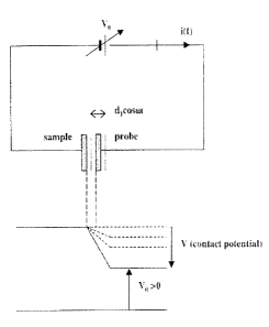
FIGURE 1 is a diagrammatic illustration of the measurement of
contact potential difference CPD used in the process of the present invention;
FIGURE 2 is a schematic drawing of the instrument used in the
specific experiments described below;
FIGURES 3A and 3B are depictions of tandem measurements of
topography and CPD;
FIGURES 4A and 4B are tandem and topographical CPD images
of a bare silicon wafer used in experiments described below, as
oligonucleotide
substrates;
FIGURES 5A and 5B are CPD images of surfaces measured as
described in the "experimental" section below;
FIGURES 6Aand 6B are fluorescence images and derivations
therefrom, from the 'experimental' section below.
Work Function and Contact Potential Difference
When an electron is removed from a point within a material, the total
change of thermodynamic free energy of the whole system is the difference
between the change of the electrochemical potential of that material and the
change of the electrostatic potential of the electron. If the electron is
removed to
a point in vacuum, far from the outside surface so the surface forces have no
more
influence, this change of free energy is called the work function of that
surface.
The corresponding change when the electron is removed to another material that
is in intimate electrical contact and thermal equilibrium with the first, is
called the
contact potential difference (CPD). For example, when two different conductors
are
first brought into electrical contact, free electrons flow out of the one with
the
higher electrochemical potential (i.e. Fermi level) into the otter conductor.
This net
flow of electrons continues until equilibrium is reached when their
electrochemical
potentials have become equal. The metal of higher work function (having
originally
a lower electrochemical potential) acquires a negative charge, the other
conductor
CA 02309412 2000-OS-24
-4-
being left with a positive charge. When the whole system reaches thermodynamic
equilibrium, the resulting potential difference is the CPD and is equal to the
difference between their work functions.
In order to measure the CPD it is necessary to connect the
conductors. A direct measurement with a voltmeter included in the circuit is
not
possible, since this can read only the algebraic sum of all the CPDs in the
circuit,
which is zero. Contact potential difference cannot be measured directly by any
type
of voltmeter, so this parameter must be measured in an open circuit, i.e.
using a
dielectric such as vacuum or air between the two ends of the above conductors.
Development of the Scanning Kelvin Microprobe
The instrument developed and used in the present invention
comprises a vibrating tip (guarded microelectrode having the apex radius of
curvature in the 50 nm range) with a known work function (tungsten), which
explores, point by point, the surface of the sample, extracting the Kelvin
current
from the local capacitor formed under the tip. When thermodynamic equilibrium
is
established, a CPD appears between the two "plates" as a voltage V and the
capacitor is charged (Figure 1 ). Since V remains constant, but the distance
between the tip and the sample changes, the charge on the plates changes too.
The tip has a sinusoidal vibration, so the separation distance between plates
is:
d (t) = do + d, cos ~t (1 )
where do is the rest position and d, is the amplitude of the vibration. The
frequency of the vibration is set at f,=2kHz.
The capacity is then:
EA _ sA
C(t) = d(t) do + d, cos ~2
CA 02309412 2000-OS-24
-S-
An adjustable do voltage source (Vo) is inserted in the circuit. The capacitor
charging process causes a current in the measurernent device, the Kelvin
current:
a(t) - dQ(t) - (y + y ~'~el, A sin apt 3
dt °)(d° +d, cos~t)z ( )
If the contact potential is compensated by the variable voltage
source, there will be no current flowing in the circuit. This compensation
(illustrated
in Figure 1 ) is detected as a null-condition by a sensitive lock-in
amplifier.
The schematic of the instrument developed and used in the present
invention is shown in Figure 2. A tip holder attaches the tip to a tube
piezoelectric
element vibrating at f,. The micropositioning system (Physiklnstrumente,
Germany)
moves the scanning table on x and ydirections with a coarse resolution of 100
nm
(closed loop DC motor) and a fine resolution of 5 nm (closed loop PZT drive).
A
piezoelectric translation stage mounted on the scanning table moves the sample
towards the tip, so the distance remains constant all the time.
The resulting current is measured by means of an ultralow-noise
charge amplifier (A250 + A275, Ampfek Inc. USA), and a lock-in amplifier
(SR530,
Stanford Research Systems, USA) tuned to f,. Automated monitoring of the
contact potential is achieved by a returning the output voltage of the lock-in
amplifier in a feedback loop.
The sample-tip distance is monitored via capacitive control at a
frequency well above the vibration frequency f,. A small ac voltage (100mV at
frequency f2= 100KHz) is added in the circuit and the resulting current
between tip
and sample is detected by a second lock-in-amplifier (of the same type) tuned
to
f2. The tip-sample capacitance is kept constant by returning the output signal
of
this lock-in amplifier to the translation table moving vertically. This signal
is used
to obtain the topographical image of the sample.
Noise and stray capacitance problems, in a preferred embodiment
CA 02309412 2000-OS-24
-6-
of the invention, are solved by using an elaborated guard electrode on the tip
and
by carefully shielding of connecting leads and all metallic surfaces.
A measure of the capabilities of the instrument can be viewed in
Figures 3A and B which show a tandem measurement of topography and CPD.
Figure 3A depicts a topographical image of the edge presented by a layer of
aluminum deposited on a silicon wafer in a typical microelectronic fabrication
process. The edge is supposed to be vertical with a steep height of about 1
Vim.
This particular topographical image was realised at a spatial resolution of 2
Vim.
Note that the second axis represents (in V) the displacement of the
piezoelectric
table and for 1 V the piezoelectric material expands 20 Vim. Accordingly, the
aluminum layer appears to have a surface height variation of about 400nm
(0.02V). Secondly, it can be seen that the edge actually slopes over 20~m (x-
axis).
The tandem CPD image is shown in Figure 3B. Note here that the image is both
rotated at 90° and inverted in order to highlight the difference in
contact potential
between aluminum and silicon (the flat, bottom surface situated at 1.5 V CPD
is the
aluminum surfiace). The technique as described herein does not generate
absolute values of contact potential difference. Accordingly, the z-axis
represents
a relative scale of CPD values. These same points for the tandem topography
and
CPD images are reflected in subsequent results.
The invention is further described for illustrative purposes in the
following experimental accounts. It is to be understood, however, that the
precise
nature of the instrument used and described herein is illustrative onle, and
the
process of the invention is not limited to any specific type or embodiment of
SKM
instrument.
Reagents
w-Undecanoyl alcohol 98%, 6,6'-dithiodinicotinic acid, trifluoroacetic
anhydride 99%, hydrogen hexachloroplatinate (IV) 99.99%,
octadecyltrichlorosilane (OTS), trichlorosilane 99%, 3-
CA 02309412 2000-OS-24
mercaptopropyltrimethoxysilane (MPS), N-bromosuccinimide (NBS), 1,1'-
azobis(cyclohexanecarbonitrile) (ACN), and dimethylformamide-sulfurtrioxide
complex were obtained from Aldrich and used as received. Various common
solvents and chemicals were obtained from BDH and used without further
treatment unless otherwise indicated as follows. Dichloromethane and
acetonitrile,
toluene and pyridine were distilled over P205, Na and KOH, respectively, and
benzene and DMF were dried over molecular sieves before use.
Silicon wafers obtained from International Wafer Service were
supplied approximately 0.4 thick and were polished on one side to a mirror
finish.
They were cut to a size of about 1 x 1 cm using a diamond-tipped pencil.
Syntheses
1-(thiotrifluoroacetato)-11-(trichlorosilyl)-undecane (TTU) was
synthesized and characterized as described previously'6-'9. The sodium salt of
2.5-
bis(bromomethyl) benzensulfonate (BMBS) was produced by bromomethylation
of p-xylene followed by conversion to the sulfonate (sodium salt) with DMF-
sulfurtrioxide reagent and NaOH.
Oligonucleotide syntheses of the following sequences 5'-HS-C6-
TATAAAAAGAGAGAGATCGAGTC-3' (F,) and its single strand, un-thiolated
complement (F2), were performed using standard CE phosphoroamidite chemistry
with conventional Applied Biosystems Inc. reagents. In order to produce the
thiol-
group containing oligonucleotide, an iodine solution was employed in
conjunction
with 3'-thiol modification cartridges (Glen Research). The oligonucleotides
were
purified using standard procedures with Poly-Pak cartridges purchased from
Glen
Research. The final products were checked for purity by HPLC and stored in 20%
acetonitrile, in polypropylene vials. Solutions of F, were treated with a ten-
fold
excess of BMBS at neutral pH in order to produce an oligonucleotide-linker
complex.
CA 02309412 2000-OS-24
_$_
Procedures
Silicon surfaces were silanized in a dry box for 2 hours with 2 ml of
a 10-3 M solution in dry toluene of a mixture of 30% TTU / 70% OTS. The TTU
coated wafers were treated with hydroxylamine in water (pH 8.5) for 2 hours to
effect deprotection of the thiol group. The F, oligonucleotide was attached to
the
surface via the linker BMBS as described elsewhere'9. Hybridization of the
surface=
bound oligo with its complementary strand was effected in pH 7.5 buffer at
room
temperature.
DNA microarray
A glass substrate containing partially-hybridized DNA associated with
examination of the yeast genome through variable size DNA probes was obtained
by donation. This microarray, produced by robotic printing, consisted of 6400
probe
domains of 150 x 150 ~m dimension spaced by 200 pm gaps.
Surface immobilized 25-mer oligonucleotides
The silane employed in the present experiments, to increase nucleic
acid surface density, TTU, attaches to hydroxylated substrates by a self-
assembly
process to produce a near monolayer-like array ofthiol functionalities
(following de-
protection of the sulfur-containing moieties). Dilution with OTS serves to
minimize
thiol-group cross linking interactions, and the use of a linking agent that
forms
disulfide bonds such as BMBS was found to optimize surface density of 11-mer
oligonucleotides at about 50 pmol cm-Z on silicon wafers'9. The capabilities
of the
SKM instrument described herein, for surface analysis at various stages of the
attachment of oligonucleotides to a silicon substrate, was tested. Duplex-
formation
between oligonucleotides was also investigated.
The tandem topographical and CPD images obtained at 20 pm spatial
resolution for the bare silicon wafer, later to be used for the immobilization
of
CA 02309412 2000-OS-24
-9-
nucleic acid, are shown in Figures 4A and B, respectively. These images serve
as a control for any changes produced by subsequent surface chemical
treatments. With respect to the topographical image, the picture was recorded
viewing from the y-axis in order to isolate an obvious fissure ofdepth about
800 nm
(width at half-depth is 100 mm). Aside from this structure, which is likely
related to
scratching connected to a polishing protocol, the surface height variability
is of the
order of 300 nm (0.15 V). The image also exhibits fairly uniform "peaks" with
a half-
height dimension of about 100nm. These characteristics are expected from a
substrate surface that is considered to be optically flat. The CPD image shows
a
quite narrow range of surface variability of approximately of 75 mV, which is
likely
connected to differences in the level of oxidation andlor contamination from
adventitious carbon. Note that the features on terms of spatial
characteristics
reflect the same overall picture as shown for the topographical image.
With respect to the use of Kelvin probe measurements to distinguish
oligonucleotide and DNA duplex formation, the 25-mer probe, F,, with BMBS
linker
in place, attaches to the de-protected TTU monolayer on the Si wafer through
formation of a disulfide bond. Using this approach, the probe is disposed
closer to
the substrate surface at the 5'-end, whereas the 3'-terminus faces away from
the
interface. Experience has shown that the surface packing density attainable by
this
attachment protocol is of the order of 20 pmol cm-2. This value implies that
the
surface density of attached nucleic acid is in the region of 1 molecule per 10
square nanometers. The precise orientation of the probe is unknown in terms of
the air-to-solid interface. The CPD image for Si surface-attached F, is
depicted in
Figure 5A (1 mm resolution). The surface variability is in the range of about
100
mV with the mean value being 1.70 V. This represents a shift of approx. 80 mV
per
the average CPD value for the bare Si surface. There are "peaks" depicted in
the
image with widths at half-height of about 7mm (spaced by lOpm). The CPD image
of the same surface for F2 hybridized to F, is given in Figure 5B. The overall
surface variability and features are much the same as for the single strand 25-
mer
attached to the substrate, but the CPD value has shifted upward by over 200
mV.
This result clearly indicates that detection of duplex formation by the Kelvin
probe
CA 02309412 2000-OS-24
- 10-
is feasible. Since the attainable resolution in relative CPD value is 1 mV,
this result
implies that high discrimination of the level of duplex formation connected to
mismatches etc. is feasible.
DNA microarrays were used in preliminary experiments, to compare
fluorescence microscopy and the SKM as detecting methods for DNA hybridization
on gene chips. Figure 6A shows a fluorescence image of typically hybridized
probe
domains and indicates the area of 5 x 5 points subsequently investigated by
the
SKM. A 20 ~m lateral resolution was chosen this time because a 1 ~m or 100 nm
resolution would be useless on the 150 ~m DNA spots. A better resolution is,
however, extremely appealing if a much higher deposition density of DNA
strands
is envisaged. Figure 6B shows one of the lines with its 5 DNA islands spaced
at
200 ~.m and some of the points above. The first 4 islands have the same CPD
value situated in the range 5.5-5.68 V; the 5'" island clearly presenting a
higher
CPD level around 6.2 V. Matrix transposition causes a reversion of the actual
image. Taking this into account, the second line of the quadrant indicated in
Figure
6A matches the SKM line shown in 6B. However, using an extremely accurate
micropositioning device that will follow the exact pattern of DNA deposition
(or
alternatively replacement of the microfluidic deposition head by an SKM
microprobe) one can assess directly DNA hybridization on microarrays, without
using the time-consuming intermediate steps. This provides higher accuracy
than
is possible with present-day conventional fluorescence microscopy.
There exists the possibility of sample alteration due to the
application of an electric field on the surface. Force microscopes operating
in the
Kelvin mode 2°-22 require a large ac voltage modulation between tip and
sample in
order to obtain the desired sensitivity to variation in the contact potential
signal:
typically several volts modulation for a 1 mV sensitivity. For a sample-tip
distance
of 10 nm, the electric field generated can reach 109 V/m (for a 10 V
modulation).
Such strong fields affect the electrostatic conditions at the surface of the
sample,
as clearly observed by consecutive measurement made with the instrument
described herein, first with force microscopy simulated conditions (with 10 V
CA 02309412 2000-OS-24
- 11 -
applied on the probe), second in normal operation (not exceeding 100 mV which
are needed for obtaining the voltage modulation). The comparative experiment
clearly shows an altered surface potential image due to the application of the
strong electric field, both on CPD image and on topography. This means that
aside
from electrostatic alteration, some local alteration of spatial configuration
of
biomolecules deposited on surfaces also occurs. From this specific point of
view,
therefore, the SKM represents a serious alternative for consideration.
The results reported herein indicate the advantages that SKM
technology presents over conventional fluorescence microscopy for the
detection
of microarray duplex formation. The technique provides direct information,
thus
avoiding the necessity to employ tagging agents. Furthermore, much higher
lateral
resolution can be achieved compared to the spatial limits imposed by the use
of
light-based technology. This, in turn, leads to the possibilities of the
analysis of
microarrays at a much higher domain density, and for the characterization of
the
true homogeneity of layer structures with dimension on the order of 50-100 ~.m
dimensions. At the present time, however, it is not possible to generate
domain
sizes down to the 1 ~m level or lower because of the inherent limitations
associated with spreading phenomena in robotic printing. There is no doubt
that
the photolithography-combinatorial synthesis of oligonucleotide arrays renders
mm-sized structures as feasible, but this configuration, by definition, is
restricted
to the use of relatively short oligonucleotides (e.g. approx. 20 mers).
While specific methods of attachment of oligonucleotides to substrate
have been described herein and used in the experimental examples, it is to be
understood that this is by way of illustration, and the invention is not
limited
thereto. It is of general application to the detection of surface-bound DNA
interaction with probe DNA, using SKM principles. For example it can be used
to
analyze nucleic acid - surface binding through interaction of chemisorbed
neutravidin with biotinylated oligonucleotide'8, and other similar binding
systems.
It can also be used generally with biochemical molecule-biochemical molecule
interactions, not restricted to DNA hybridization, e.g. in determining
potential drug.-
receptor interactions and bindings.
CA 02309412 2000-OS-24
-12-
References
1. L-E. Cheran, H-D. Liess, M. Thompson, The Analyst, 1999, 124, 961
2. W. Nabhan, B. Eqer, A. Broniatowski and G. De Rosny, Rev. Sci. lnstrum.,
1997, 68 (8), 3108
3. M. Schmidt, M. Nohlen, G.,Bermes, M. Bomer and K. Wandelt, Rev. Sci.
Instrum., 1997, 68, 10, 3866
4. M. Bomisch, F. Burmeister, A. Rettenberg, J. Zimmermann , J. Boneberg
and P. Leiderer, J. Phys. Chem. 8, 1997, 101, 10162
5. W.A. Zissman, Rev. Sci. Insfrum., 1932, 3, 367
6. P. Craig and V.Radeka, Rev. Sci. Instrum., 1970, 41, 2, 258
7. N.A.Surplice and R.J. D'Arcy, J.Phys.E: Sci. lnstrum., 3, (1970), 477
8. B. Ritty, F. Watchel, R. Manquenouille, F. Ott, J. Bonnet, J. Phys. E:
Sci.lnstrum., 15, 1982, 310
9. I.D. Baikie, E. Venderbosch, Rev.Sci.lnstrum. 62 (3), 1991, 725
10.O.A. Semenikhin, L.Jiang, T. lyoda, K. Hashimoto, A. Fujishima, J. Phys.
Chem. 100, 48, 1996, 18603
11. I. Samec. W. Johnson, M. Cappadonia, M.Jauch, K. Doblhofer, Sensors and
Actuators, 8, 13-14 (1993) 741
12. S. Lundgren, B. Kasemo,Rev. Sci.lnstrum. 66, 7, (1995) 3976
13. C. S. Kumar, A. Subrahmanyam, J. Majhi, Rev. Sci. Instrum. 67 (3) (1996),
805
14. H.A. Engelhardt, P. Feulner, H. Pfnur, D. Menzel, J. Phys E: Sci. Instr.
19,
(1977), 1133
15. LD. Baikie, G.H. Bruggink, Mat. Res. Soc. Syrup. Proc. 309, (1993), 35
16. M. E. McGovern, M. Thompson, Can.J.Chern. 77 (1999), 1678
17. L.M. Furtado, H.Su, M. Thompson, D.P. Mack, G.L. Hayword, Anal. Clzern. 7,
(1999), 1167
18. M. E. McGovern, M. Thompson, Anal. Chem. Submitted
20. M. Nonnenmacher, M.P. O'Boyle and H.K. Wickramasinghe, Appl.
CA 02309412 2000-OS-24
-13-
Phys, Lett., 1991, 58, 25, 2921
21. M. Nonnenmacher, M.P. O'Boyle and H.K. Wickramasinghe,
Ultramicroscopy, 1992, 42-44, 268
22. M.Yasutake, J. Appl. Phys., 1995, 34, 3403
23. M.Yasutake, A.Daisuke and M. Fujihira, Thin Solid Films, 1996, 723,
279
Figure captions
1o Figure 1: The principle of the Kelvin method: the Kelvin current
appears in the circuit due to the sinusoidal movement of the "probe"
plate of the local capacitor formed between tip and sample and is a
measure of the difference in Fermi levels between the two materials
(CPD)
Figure 2: Block-diagram of the instrument
Figure 3A: Topography of patterned aluminum deposition on a silicon wafer
(proposed 1 ~m step)
Figure 3B: Contact potential image of the same step
Figure 4A: Topography of a prepared silicon surface before DNA deposition
Figure 4B: Contact potential image of the same area
Figure 5A: Contact potential image of oligonucleotide (F,) attached to Si
surface
Figure 5B: Contact potential image of F,:F2 duplex
Figure 6A: Confocal fluorescence microscope image of a DNA microarray
Figure 6B: SKM image of a selected area on the microarray