Note: Descriptions are shown in the official language in which they were submitted.
CA 02309450 2000-OS-02
WO 99/24823 PCT/US98I23547
~ANOELECTRODE ARRAYS
This application claims the benefit of U.S. Provisional Application No.
60/065,373 filed
November 12, 1997.
The present invention relates generally to methods and apparatus for detecting
and
characterizing single biological molecules in solution and, more specifically,
to detect and
characterize individual proteins, protein mixtures, DNA or other molecules on
a chip.
BACKGROUND OF THE INVENTION
The characterization and quantification of individual proteins or complex
biological
molecules is extremely important in fields as distant as medicine, forensics
and the military.
For example in medicine the presence and concentration of given proteins can
be used for
disease or pre-disease diagnoses. In the military given proteins can be used
to signal the
presence or absence of given pathogens in the environment which is extremely
important for
example in potential germ warfare situations.
The detection of individual proteins or molecules in biological samples is
currently
complex and generally requires sophisticated and bulky equipment.
Several technologies have recently been disclosed to characterize given
biological
molecules. In particular success has been achieved in high density DNA chips
build by
Affymetrix as originally described in PCT International Publication No. WO
90/15070.
U.5. Patent 5,624,537, entitled "BIOSENSOR AND INTERFACE MEMBRANE," describes
a
1
CA 02309450 2000-OS-02
WO 99124823 PCT/US98/23547
protein-receiving matrix and a single electrode.
U.5. Patent 5,395,587, entitled "SURFACE PLASMON RESONANCE DETECTOR HAVING
COLLECTOR FOR ELUTED LIGATE," describes a system to measure immobilized
ligands using
a plasmon resonance detector.
U.5. Patent 5,607,567, entitled "PROTAMINE-RESPONSIVE POLYMERIC MEMBRANE
ELECTRODE," describes a membrane electrode.
U.5. Patent $,328,847, entitled "THIN MEMBRANE SENSOR WITH BIOCHEMICAL
SWITCH," describes a biosensor with a specific recognition biomolecule.
U.S. Patent 4,777,019, entitled "BIOSENSOR," describes a biosensor for
biological
monomers.
U.5. Patent 5,532,128, entitled "MULTI-SITE DETECTION APPARATUS," describes
test
wells combined with electrodes to detect given biological molecules.
U.5. Patent 4,983,510, entitled "ENZYMES IMMOBILIZED ON LATEX POLYMER
PARTICLES FOR USE WITH AN AMINO ACID ELECTROSENSOR," describes an
electrosensor with
a latex polymer trap.
U.S. Patent 5,384,02$, entitled "BIOSENSOR WITH A DATA MEMORY," describes a
membrane biosensor with a memory module.
U.5. Patent 5,567,301, entitled "ANTIBODY COVALENTLY BOUND FILM IMMUNOBIO-
sENSOR," describes an antibody biosensor.
U.S. Patent 5,310,469, entitled "BIOSENSOR WITH A MEMBRANE CONTAINING
BIOLOGICALLY ACTIVE MATERIAL," describes a membrane biosensor.
U.5. Patent 5,019,238, entitled "MEANS FOR QUANTITATIVE DETERMINATION OF
ANALYTE IN LIQUIDS," describes a means to sequentially test the ionic
concentration of fluids.
2
CA 02309450 2000-OS-02
WO 99124823 PCT/US98/23547
U.S. Patent 4,981,572, entitled "ELECTRODE UNIT AND PACKAGE FOR A BLOOD
ANALYZER," describes an electrode and apparatus to analyze blood.
U.5. Patent 4,452,682, entitled "APPARATUS FOR MEASURING CLINICAL EMERGENCY
CHECK ITEMS OF BLOOD," describes an apparatus to measure multiple elements in
blood.
U.S. Patent 4,568,444, entitled "CHEMICAL SUBSTANCE MEASURING APPARATUS,"
describes an electrode to quantify chemical substances in a solution.
U.5. Patent 5,2$1,539, entitled "IMMUNOASSAY DEVICE FOR CONTINUOUS MONI-
TORING," describes a two step immunoassay device.
U.5. Patent 5,192,507, entitled "RECEPTOR-BASED BIOSENSORS," describes a
biosensor
based on a polymeric film to detect opiates.
U.5. Patent 5,156,810, entitled "BIOSENSORS EMPLOYING ELECTRICAL, OPTICAL AND
MECHANICAL SIGNALS," describes a thin layer biosensor.
U.5. Patent 5,494,831, entitled "ELECTROCHEMICAL IMMUNOSENSOR SYSTEM AND
METHODS," describes an immunologic biosensor.
U.5. Patent 5,332,479, entitled "BIOSENSOR AND METHOD OF QUANTITATIVE ANALYSIS
USING THE SAME," describes an electrode based sensor with a biologically
active receptor.
U.5. Patent 5,582,697, entitled "BIOSENSOR, AND A METHOD AND A DEVICE FOR
QUANTIFYING A SUBSTRATE IN A SAMPLE LIQUID USING THE SAME," describes a
biosensor
based on the measure of reduction between a substrate and an oxidoreductase.
U.S. Patent 4,908,112, entitled "SILICON SEMICONDUCTOR WAFER FOR ANALYZING
MICRONIC BIOLOGICAL SAMPLES," describes a micro capillary separation device
with detector
capabilities.
U.5. Paterit 5,409,583, entitled "METHOD FOR MEASURING CONCENTRATIONS OF
3
CA 02309450 2003-02-18
774J2-45,iS)
SUBSTRATES IN A SAMPLE LIQUID BY USING A BIOSENSOR," describes a two step
biosensor.
U.S. Statutory Invention H201, entitled "B10SENSORS FROM MEMBRANE PROTEINS
RECONSTITUTED IN POLYMERIZED LIPID B1LAYERS," describes a method for
incorporating and
using cell membrane proteins in biosensors.
The above described technologies are generally used for the detection of a
single type
or a few different types of molecules. None of these technologies are
particularly adapted to
allow a very large number of different types of proteins, protein variants or
other biological
molecules to be detected and quantified simultaneously on a single chip.
Furthermore, none
of the prior art provides a suitable technology to directly build protein-
specific electronic
receptors on a chip without the use of any biological binding agents,
synthetic probes or
complex micro-structures such as test wells.
We disclose herein a novel, smaller, faster and more cost effective technique
to detect,
characterize and quantify individual proteins or other complex molecules on a
chip. The
technology described herein may also serve as a new method for DNA sequencing.
4
CA 02309450 2003-02-18
.r
7740'2-4~yS)
SU~iARY OF THE INVENTION
According to one aspect of the present invention,
there is provided a sensor for detecting biological
molecules, said sensor comprising: a substrate; an electrode
having the capacity to bind a preselected biological
molecule, said electrode having between about 10-9 and 10-10
meters in height and width.
According to another aspect of the present
invention, there is provided a sensor for detecting
proteins, said sensor comprising: a micro-capillary tube; a
plurality of electrodes disposed in said tube, said
electrodes having the capacity to bind a preselected
protein, said electrodes being between about 10-9 and 10-l0
meters in height and width.
According to still another aspect of the present
invention, there is provided a sensor for detecting
biological molecules, said sensor comprising: a substrate; a
micro cantilever array on said substrate; at least one
electrode disposed on at least one of said micro
cantilevers.
According to yet another aspect of the present
invention, there is provided a sensor for detecting a
biological molecule, said sensor comprising: a
microcantilever, wherein at least one electrode comprises a
height and width and length disposed on the microcantilever,
wherein the at least one electrode disposed on the
microcantilever is adapted to interact with and bind to a
concentration of a biological molecule; and further
comprising at least one from the group consisting of a
capacitive means, an electron tunneling means, a laser
means, a piezoresistive means, a piezoelectric means, a
4a
CA 02309450 2003-02-18
774.0'2-4~'~S)
resonance frequency shift means and a x-y positional
fluorescence means for detecting the concentration of the
biological molecule adapted to bind to the at least one
electrode, and wherein the microcantilever has a plurality
of electrodes disposed thereon forming a cluster, each
electrode having varying dimensions adapted to bind the
cluster with biological molecules and for detecting
concentrations thereof.
According to a further aspect of the present
invention, there is provided a sensor comprising: a base; a
microcantilever integrally attached to the base; and at
least one electrode disposed on the microcantilever, wherein
the electrode extends from a principal surface of the
microcantilever a distance of from about 2 Angstroms to
about 5 nanometers, the electrode having a width of from
about 2 Angstroms to about S nanometers.
According to yet a further aspect of the present
invention, there is provided a method of sequencing nucleic
acids, comprising the steps of: providing a sensor, said
sensor having a substrate on which plurality of electrodes
are disposed, said electrodes each being between about 10-9
and 10-1° meters in height and width; contacting said
electrodes with a solution containing nucleic acids; said
electrodes having the capacity to bind at least some of said
nucleic acids.
According to still a further aspect of the present
invention, there is provided a method for producing a sensor
comprising: providing a microcantilever, the microcantilever
having at least one electrode disposed on the
microcantilever wherein the electrode extents from a
principal surface of the microcantilever a distance of from
4b
CA 02309450 2003-02-18
.r
774~0'2-45,f S)
about 2 Angstroms to about 5 nanometers, and a width of from
about 2 Angstroms to about 5 nanometers.
According to another aspect of the present
invention, there is provided a silicon chip to detect
individual proteins comprising at least one sensor
manufactured with Angstrom level precision where the surface
of the sensor complements exactly the three dimensional
shape of a given protein.
In one aspect the present invention provides a
sensor which is capable of distinguishing between different
molecular structures in a mixture. The device includes a
substrate on which nanoscale binding sites in the form of
multiple electrode clusters are fabricated. Each binding
site includes nanometer scale points which extend above the
surface of a substrate. These points are preferably
nanoelectrodes which are spatially configured to provide a
three-
4c
CA 02309450 2000-OS-02
WO 99/24823 PCTIUS98/23547
dimensional electro-chemical binding profile which mimics a chemical binding
site. Thus, the
binding sites have selective affinity for a complementary binding site on a
target molecule or
for the target molecule itself.
In one aspect, the binding sites are arranged in an array on the substrate. In
one aspect,
the spatial and electro-chemical profiles of each site of the array are
identical and provide an
assay for a single target molecule. In another aspect, regions of the
nanoelectrode array carry
grouped arrays of electronically and/or spatially distinct binding sites for
simultaneous detection
and quantification of several molecular species.
In still another aspect, the materials used for the electrodes and surrounding
surfaces are
selected based on preferred intrinsic electrical and chemical properties.
The nanoelectrode array may be included in a chamber which can retain fluids.
Several
arrays may be used in a single chamber and several different chambers may be
used on a single
chip.
In still another aspect, the nanoelectrode array and chamber are attached to
at least one
micro-fluidic delivery and separation system such as a micro-capillary which
allows both the
delivery and separation by size and electrical properties of the proteins or
other molecules to
be analyzed.
In another aspect, a microcontroller or microprocessor is provided to analyze
signals
CA 02309450 2000-OS-02
WO 99/24823 PCT/US98I23547
from the nanoeLectrodes and/or to time and control the fluidics separation of
the-molecules or
proteins.
In another aspect, the chip with the nanoelectrode arrays is associated with
an electronic
temperature control system such as a thermoelectric device having a thermistor
to vary the
bonding kinetics or the electro-chemical affinity of the molecules with given
nanoelectrodes,
as well as the flow kinetics and separation of the molecules.
In another aspect, the nanoelectrodes are interspaced in a linear microtube to
sequence
DNA.
Thus, it is an object of the present invention to provide a novel and rapid
method to
analyze small biological molecules in solution such as proteins and to
sequence DNA by using
semiconductor chip technology with extremely high packing densities.
It is a further object of the present invention to ensure that the entire chip
can be easily
integrated into devices for automated analysis of proteins, DNA or other
molecules.
BRIEF DESCRIPTION OF THE DRAWINGS
FIG. 1 is a perspective diagrammatic view of a nanoelectrode array showing
different
nanoelectrode clusters.
FIG. 2 is a side elevational diagrammatic view of a protein-specific
electronic receptor
6
CA 02309450 2000-OS-02
WO 99/24823 PCT/US98/23547
and its matching protein.
FIG. 2A is a side elevational cross-section of a protein-specific electronic
receptor and
its matching protein.
FIG. 3 is a side elevational cross-section of a nanoelectrode array inside a
micro-fluidic
tube, showing the trapping of a specific protein on its corresponding
nanoelectrode receptor.
FIG. 4 is a diagrammatic side elevational cross-section of a microtube with a
linear
nanoelectrode array to detect DNA.
FIG. 5 is a cross-section of an integrated chip with nanoelectrode arrays, a
micro-fluidic
delivery system and associated electronics.
FIG. 6 is a side elevational cross-section of a nanoelectrode receptor showing
the
electrical field which is broken or modified upon binding of a specific
molecule to said
receptor.
FIG. 7 is a view of a cantilevered nanoplate with several identical
nanoelectrode
clusters.
D~T.~H~ED DESCRIPTION OF THE PREFERRED EMBODIMENTS
The present invention is based in part on the fact that recent advances in
technology
7
CA 02309450 2000-OS-02
WO 99/24823 PCTIUS98/2354~
such as the use_of scanning tunneling microscopy (STM) has demonstrated that
ultra small
structures of a single or a few atomic layers can be built on a semiconductor
surface such as
silicon. Because of the size of these structures, they are generally referred
to as nanostructures
(one nanometer or nm = 10'9m, 1 Angstrom or ~r = 10''°m). These
structures can be as small
as a few Angstroms in diameter which is well below the Stokes radius of a
small protein (which
is approximately 25-35~}. Since these structures can be built using different
chemical elements
(or the voltage applied to the structure can be selectively varied) and the
spacial distribution,
height width and shape of the structures can also be varied, these structures
can be built in
clusters to serve specifically as "molecular electrodes" whose electro-
chemical properties and
spacial distribution can be made to correspond precisely with the external
three dimensional
shape and electro-chemical properties of molecules, preferably biochemicals
and most
preferably proteins. Therefore each of these clusters can serve as individual
electronic protein
"receptors" (or detectors). Since a very large number of these molecular
electrodes can be
placed on a single chip, the resulting arrays, termed here "nanoelectrode
arrays" can be used to
detect, characterize and quantify many different proteins on a single chip. In
a variation of the
technology, the chip can also be used to sequence DNA.
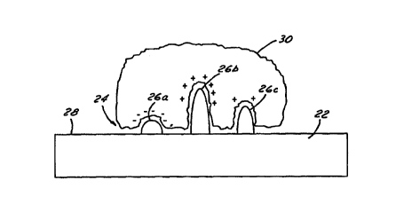
Referring now to Figure 1 of the drawings, microelectronic molecular sensor 20
is seen
having substrate 22 on which an array of binding sites or clusters 24 are
formed. Substrate 22
may comprise any number of materials such as silicon, germanium, gallium
arsenide, or other
semiconductors. Referring now to Figure 2 of the drawings, one binding site 24
is shown in
more detail having multiple electrodes 26a, 26b and 26c which are spatially
distributed to form
a pattern. Thus, it can be seen that each electrode 26a, 26b and 26c in this
particular
8
CA 02309450 2000-OS-02
WO 99124823 PCT/US98I23547
embodiment is spaced laterally from the adjacent electrode and is elevated at
different heights
off principal surface 28 of substrate 22.
It will be appreciated that through molecular modeling and empirical data, the
topology
of the binding sites and electrical charge are tailored to provide the
required electrical and
topographic properties to selectively recognize and bind a complementary
region of a target
molecule. As shown best in Figure 2, protein 30 having a defined shape
specific to that protein
attaches to a given nanoelectrode cluster composed of three nanoelectrodes
26a, 26b and 26c.
As will be explained more fully, each nanoelectrode may have slightly
different electro-
chemical properties because of differing charges and/or chemical compositions.
These
individual electro-chemical properties match not only the electro-chemical
affinities of the
amino acids or atoms present on the grooves of the protein but also complement
the shape of
the groove itself. Thus, when a molecule having the proper complementary
profile binds to
"receptor" 24 bridging the gap between the electrodes, a change in electrical
potential occurs
which can be monitored through appropriate circuitry to provide an indication
of the presence
of the target molecule.
In the most preferred embodiments of the present invention binding sites 24
have
nanoscale geometries. As illustrated in Figure 2, the distance from principal
surface 28 to the
top of electrode 26b is 1.9 nanometers, the width of electrode 26b is 0.7
nanometers and the
distance between electrodes 26b and 26c is 1 nanometer. In general, each
electrode will
typically be between 0.2 and about 3 nanometers in height and from about 0.2
to about 2
nanometers in width. As used herein "nanoelectrode" shall include atomic scale
as well as
9
CA 02309450 2003-05-09
x'7402-45 (S)
nanoscale structures, i.e. from 2A to 5 nanometers. There will also typically
be.from about 2
to about 8 separate electrodes in a°.ac:h cluster 24, lrlectrodes 26x,
26b and 26c can be formed
of a number of materials, either irnrinsic or doped, such as gold and platinum
and copper and
other electrometals. Gold is particularly preferred. Also it may be suitable
to form the
electrodes of one ma~~erial and coax the outer portion with a different
material, e.g. gold coated
with zinc oxide or gold coated with a thiol group.
The electrodes may be eaclo separately connected to a power source by small
conductive
regions or wires which may be for~~nc:d of gold. (n Figure ? A , individual
conductive layers 34x,
34b and 34c are shown electrically connecting their respective electrodes 26x,
26b and 26c.
Dielectric layers 36 electrically isc:>late the individual conductive layers
and dielectric sheaths
38 electrically isolate the individual electrodes. It will be appreciated that
different potentials
can be applied to the various indj~,-~idual electrodes and that electrodes
from different clusters
can be electrically linked to a single layer e.g., layer >4a. It will be
appreciated that the various
layers can be formed using conventional thin-filno fabrication techniques such
as CVD, thermal
growth and ion implantation.
It has been shown recentl~r tlhat electrical "wires" can be built of single
atoms (see for
example review by L.eo Kouwenh<:wf:n "Single-Molecule 7yransistors", Science,
Vol. 275, pages
1896-1897,28 March 1997) .
The wires can be deposited in a m m~ber of different ways as pan of the
microchip fabrication
process, prior to the deposition o:(~ the nanoelectrodes. The nanoelectrodes
can be deposited
directly on the chip by Scanning ~l('unneling Microscope (as described in Kolb
et al., Science,
CA 02309450 2003-05-09
77402-45(S)
Vol. 275, pages 109?-1099, ? I F~b~ruary 19?7 >. A number of other chip
fabrication methods are possible such as different Lithography techniques,
etc.
In another aspect the naraoelectrodes are not corrrtected to any electrical
wires or
conductive layers. In this case the binding of the protein or other molecule
is simply dependant
on the shape and chemical properties of the individual nanoelectrode clusters.
Defection of the
attachment of the given molecule to a given cluster can then be achieved by
means other than
electrical, for example by a highly precise x-y positionai fluorescence
reader, similar to that
used for the DNA chip technolog;~ ot' by resonance.
In case the nanoelectrodes are not connected to wires (i.e. are not "live"
electrodes), the
nanoelectrodes may in some applications be intercoru'tected in a given
cluster. In this case the
clusters would comprise intercormected peaks and grooves and these would form
a larger
structure (i.e. from , to > 10 nanorr~eters). 'this structure could be
tailored either to match
precisely the actual biological re~:eptor of the target molecule or to allow
the entire molecule
to fit into a 3-dimensional "recelator" which would match at least a third of
the overall 3-D
shape of the molecule. In some ir:~stances and depending on the overall shape
of the molecule,
the receptor that is built may not necessarily include a site corresponding to
the actual biological
receptor of the target molecule.
Several types of binding or adsorption of the molecule to the nanoelectrode
receptor are
possible, depending on the cherrtical composition of the nanoelectrodes, the
voltage and the
CA 02309450 2000-OS-02
WO 99/24823 PCTIUS98/23547
chemical to be measured. Binding forces may include covalent binding,
electrostatic binding,
hydrogen bonds and van der Waals bonds.
Depending on the type of detection that is required, the individual
nanoelectrodes of
individual clusters do not necessarily need to be composed of different
electrometals since both
the spacial distribution and the height of the nanoelectrodes can be varied
and these two
variables may be enough for specific molecule detection in given applications.
In some
applications, each nanoelectrode can be selectively charged in a given
cluster, allowing the
electro-physical property of the nanoelectrode to be varied.
The entire sensor can be built using a computer controlled operation, where
the spacing,
height, width and the composition of the nanoelectrodes can be made to
correspond exactly to
the three dimensional shape and matching electro-chemical properties of a
selected molecule.
Furthermore, since the position of the nanoelectrode clusters corresponding to
a given receptor
for a given molecule is determined during the fabrication process, this
position information can
be used to detect attachment or binding. For example, a large nanoelectrode
array can be built
with many different clusters, binding in a solution can be allowed, then the
array be read using
a highly accurate x-y reader in a way similar to the DNA chip. Computer
control fabrication
of the nanoelectrodes also allows for identical copies of the chip to be made.
It will be also be appreciated that the geometries that are built on the
surface of the chip
can be made to correspond exactly to the matching image of a crystallized
protein surface taken
from x-ray diffraction studies. Hence nanoelectrode array clusters can be
built directly using
12
CA 02309450 2000-OS-02
WO 99124823 PCTIUS98/23S47
crystallographic data and the resulting surfaces on the chip would favor
protein-specific
crystallization on given arrays.
In another aspect, since multiple identical receptors can be built on the same
chip, this
technology can be used not only to detect given molecules but also to
precisely estimate the
quantity of these molecules present in the sample by measuring binding rates
in identical
clusters.
Refernng to FIG. 3, two partial nanoelectrode arrays are shown facing each
other and
forming micro-channel or nanotube 60, which permits the flow of small
molecules such as
protein 70 therethrough. If protein 70 matches the shape of a receptor
composed of electrodes
74, 78, and 82, the physical binding of the protein will cause a temporary
minute change in the
electrical signal which can be measured simultaneously in all said
nanoelectrodes. The strength
of the electrical signal can be modified for example by adding a conductant to
the carrier
solution for the molecules which need to be studied. Alternatively the
nanoelectrodes
themselves can be charged with a small current, which would change upon
attachment of the
given molecule. Depending on the electro-chemical properties of the
nanoelectrodes and the
analyte, the temperature and the flow rate, the binding may last only a
fraction of a second or
last longer. Time of retention in itself is another important variable which
can be used in
detecting and quantifying the types of molecules present in the sample.
In some applications, micro-channel 60 can form a part of a network of
channels of
different and specific sizes, matching the sizes of the proteins to measure.
Each of these
13
CA 02309450 2000-OS-02
WO 99/24823 PCTIUS98/23547
channels can be_equipped with molecular sieves, allowing only proteins or
molecules of certain
size to pass through. The channels themselves can also serve as a means to
separate molecules
and deliver them to given detector chambers with nanoelectrode arrays which
are specifically
made to measure given classes of proteins or molecules of given molecular
weights. In this
case, each of the arrays would have nanoelectrodes with sizes corresponding to
the sizes of the
proteins to measure. As part of this network of channels, specific chambers
can be added with
specific functions such as a chamber to lyse cells. Other chambers can be
filled with specific
reagents which can be used as needed.
In another application, each of the micro-channels is equipped with only one
or a few
nanoelectrode clusters and the protein mix is flowed through each of the
channels. With the
help of a microcontroller or a microprocessor controlling the flow rate in
each micro-channel,
the signals from each of the nanoelectrode clusters is then measured combining
the power of
the following variables for detection: protein separation rates (based on the
size and charge of
the proteins) and retention time on each given cluster (based on th.e shape
and electro-chemical
properties of the molecule). Indeed, the more a given molecule matches a given
receptor, the
longer it will bind. It is obvious that the sophisticated control and measure
of the electrical
signals in each nanoelectrode (as well as the control of all other variables
such as sample flow
rates, temperature, etc.) can only be done with the help of a microcontroller
or a
microprocessor.
Refernng now to FIG. 4, a nanoarray of electrodes 90 is built in a linear
microtube 100
with the spacing and electro-chemical composition of the nanoelectrodes varied
in such a way
14
*rB
CA 02309450 2000-OS-02
WO 99/24823 PCTIUS98I23547
to correspond exactly to the distance between given base pairs of a linear
piece of DNA or RNA
110. In this case, the nanoelectrodes are built using only two variables:
precise spacing and
electro-chemical composition (not height) favoring position-specific binding
of specific base
pairs of DNA or RNA to matching nanoelectrodes. The principle that is applied
here is that
DNA is known to behave as a linear molecule when flowed in a microtube and
that this rate of
flow can be controlled and measured with precision. Furthermore, the distance
between 10
DNA base pairs being precisely 34 A, the nanoelectrodes can be spaced
precisely in multiples
of 3.4 t~ as shown in 120. By varying the spacing and charge and/or
composition of the
nanoelectrodes and by measuring the conductance changes over time in
sequentially placed
nanoelectrodes, an entire sequence is created, based on the timing of the
signals of position-
specific nanoelectrodes. The full DNA (or RNA) sequence is then reconstructed
with the help
of a microcontroller (or microprocessor) which can also control the flow rate
in the microtube.
ANALYSIS OF PROTEIN VARIANTS
Mutations or other changes in the DNA result in amino-acid substitutions in
the protein.
These substitutions in turn result in conformational shape changes in the
protein and can result
in proteins that are either non-functional or have different properties. Since
the three-
dimensional (3-D) structure of proteins can now be inferred with precision on
the basis of x-ray
crystallography or nuclear magnetic resonance (NMR), the 3-D shapes of the
protein variants
can also be generated using the same method. Hence the entire spectrum of
protein variants for
given classes of proteins can be measured and quantified using the
nanotechnology described
above. This is because the conformational changes of each protein variant can
be represented
by a given nanoelectrode cluster varying in the shape, distribution and
electro-chemical
CA 02309450 2000-OS-02
WO 99/24823 PCT/US98/23547
properties of the nanoelectrodes. In fact, the building of the arrays can
be_comput~er-controlled
and link the information matching the putative 3-D structure of proteins of
interest (and their
variants} to the micro fabrication of all the matching receptors on the chip.
By measuring and
quantifying these variants as described above, this approach represents a
powerful alternative
to direct DNA sequencing since all the possible mutation products of given
genes which are
expressed can be directly measured on a chip. Another advantage is that the
chip would be
fully reusable. Furthermore, given the extremely high density of the
nanoelectrode arrays that
can be built on a single chip, the entire spectra of protein variants for many
genes can be
measured at once on the same chip. In fact with a refinement in the
technology, all existing
human proteins and their variants could theoretically be measured on a single
chip of 1 cm2 and
the number of receptors that could be built on such a chip could theoretically
exceed 1 billion
which is a thousand fold improvement over any existing technology.
PROTEIN SEPARATION
As indicated above, the separation of molecules can be achieved by flowing
said
molecules in extremely small tubes (micro-capillaries, micro-channels or
nanotubes) where
smaller molecules travel faster than larger ones which are retained by
friction and weak bonding
interactions with the surfaces of the tubes. The result that is achieved is
equivalent to
electrophoresis but with the advantage of speed, cost and reusability of the
micro-capillary.
Refernng now to FIG. 5, micro-channel 130 is shown with a sample input port
132 and
a long loop flowing into an optional reagent micro-chamber 134, itself
connected to an optional
input port 136. Micro-channel 130 separates biological molecules by size and
charge while
16
CA 02309450 2000-OS-02
WO 99124823 PCT/US98123547
micro-chamber 134 allows the selective input of an external reagent or
solution. The flow and
on/off position at each micro-channel juncture can be controlled
electronically either by an
external micro-pump (not shown), by thermocapillary action or by a change of
electric
potential. After entering micxo-chamber 134, the analyte then flows
successfully into micro-
chambers 138a, 138b, 138c, then 138d, each holding different nanoelectrode
arrays with
nanoelectrode clusters of varying sizes and densities. In this particular
design, the
nanoelectrode arrays are fabricated immediately adjacent to a micro-
electronics multiplexing
or control area 140, itself connected to an interface 142. After reacting with
successive
nanoelectrode arrays in successive micro-chambers, the sample exits via port
146. The micro-
channels and micro-chambers can either be etched in the silicon surface itself
or can be
fabricated separately on a surface of a material like glass, diamond, plastic
or the like, which
is then attached to the silicon surface.
This design can be varied in many different ways and FIG. 5 illustrates just
one of many
possible combinations of micro-channels, nanoelectrode arrays and micro-
electronics that can
be fabricated on a chip. As indicated above, a chamber allowing the lysing of
the cells or
viruses to be analyzed can also be included on the chip. Also, it should be
indicated that the
directional flow in the micro-channels can be reversed and that each
connecting micro-channel
can be selectively opened or closed electrically. Hence, when the test is
completed the entire
system can be heated to allow protein denaturation (andlor the potential in
the nanoelectrodes
can be reversed), then the system can be flushed with a solution to clean the
nanoelectrode
arrays and allow reuse of the chip.
17
CA 02309450 2000-OS-02
WO 99/24823 PGTIUS98123547
Hence a_complete and integrated protein separation and detection systerr~ can
be built
on a single chip. An important aspect of combining nanoelectrode arrays, micro-
channels and
a rnicrocontroller (or a microprocessor) is that the time of separation (from
sample injection
into port 132 to time of first detection) and the length of retention on given
nanoelectrode
receptors are important variables for characterizing individual protein or
protein variants. For
example, the system can be calibrated by injecting known proteins, then known
mixes of
proteins, prior to injecting the sample to be tested. The time taken to reach
a given
nanoelectrode receptor and the length of binding on different electronic
receptors would be
specific to specific proteins (or to protein variants) and the signal-specific
profiles for each
protein can then be stored in memory and compared to those of the sample to be
tested.
While FIG. 5 shows an integrated design, it is obvious that the protein
separation
component and the electronic components can also be placed externally and that
the chip can
be as simple as having a single nanoelectrode array enclosed in a single
chamber with an
interface. This chip (which may be disposable) can then be inserted into a
larger module with
the above components. Also, as indicated below, other detection methods can be
used and the
design of the chip would change accordingly.
DETECTION
There are many ways in which the binding or adsorption of the analyte on the
nanoelectrode array can be detected. Refernng now to FIG. 6, one way of
detecting the signal
due to adsorption on the nanoelectrode array is by electrical signal. In this
case, at least one of
the electrodes in each cluster of a given array is used as a "source" 160
while the rest of the
18
CA 02309450 2000-OS-02
WO 99/24823 PCT/US98/23547
cluster 165 is used as a "sink." When an analyte, say a protein, is adsorbed
it changes the flow
of the current (pico ampere) as shown in FIG. 6. The electrodes are isolated
by a layer of oxide
170. The unwanted effects of the electrical current can be avoided by using an
AC approach.
Referring now to FIG. 7, the second approach for detection of binding is by
using a
resonance approach. In this method, a nano structure is constructed. For
example, nanoplate
180 of the dimension less than one micron is built. This structure can be free
standing or it can
be cantilevered. Identical sets of nanoelectrode receptors 24 are then
fabricated on this surface.
The structure is designed to have resonance frequency in the MHz to low GHz
region. As the
analyte flows past these structures, they spend a longer time on the
cantilever if they have a
structure that is complementary to the nanoelectrode structure. In other
words, the analyte
molecules undergo collision with the nanoplate. If there exists any
complimentary nature
between the analyte and the substrate, the analyte will spend more time on the
surface during
collision. This can be detected optically by shining a laser diode on the
structure and detecting
the reflected signal using a position sensitive photodiode. The AC signal in
the photodiode
shows the resonance response of the structure. The greater the signal, the
larger the
concentration of bound biological molecules, i.e. the greater the
concentration of the said
molecule in the solution. Other detection techniques such as capacitive,
piezoresistive,
piezoelectric, electron tunneling, etc. could also be used.
The structure can be excited into resonance response by mechanical means using
a
piezoelectric element. In this technique, a nanoplate structure is attached to
a piezoelectric
material which can be vibrated using an AC signal. At resonance the structures
oscillate with
19
CA 02309450 2000-OS-02
WO 99124823 PCTIUS98/23547
maximum amplitude. It can also be excited into resonance by modulating the
diode laser using
square wave power pulses. Since square waves contain all the Fourier
components, there will
be a component that corresponds to the resonance frequency of the structure.
Since these nanoelectrodes can be constructed on geometrical structures with
extremely
small thermal mass (for example, nanoplates have a thermal mass of the order
of many
picograms or less), they can be heated and cooled in the micro to milliseconds
time frame. This
fact can be used to adsorb and desorb analytes in a periodic fashion. However,
when there is
a complimentary structure between surface and the analytes the desorption time
scale will be
different.
USE OF AN EXTERNAL DETECTOR
In another detection application the entire chip which has been allowed to
react with the
sample is placed in a x-y laser reader in a manner similar to the DNA chip. In
this case, the
chip is incorporated into a highly precise holder to ensure accurate position
reading of each
cluster. Detection may be done by fluorescence, for example after reaction of
the bound
samples to the clusters with a fluorescent molecule or with labeled
antibodies.
Detection may also be done by other means such as laser-desorption-ionization
mass
spectrometry.
NANOELECTRODE CONSTRUCTION
Nanoelectrode arrays can be constructed on a doped semiconductor substrate by
CA 02309450 2000-OS-02
WO 99/24823 PCT/US98/23547
nanolithography using scanning probes. In this approach, metal clusters are
deposited either
from a solution or by field evaporation from a STM/AFM tip. Since the electric
field between
the tip and the substrate is very high (109V/m), many metals can be field
evaporated. In
solution many metals can be electrochemically deposited on a surface. The
surface of the
semiconductor can be oxidized to be an insulator.
Nanometer scale trenches and lines can be made on a semiconductor surface
using STM
tip in an oxide etching solution producing a trench. The depth of the trench
depends on the
time spent by the tip at that location and the voltage on the tip. Hence, not
only can the
nanoelectrodes be built by deposition, but they can also be built by etching.
The trenches can
also be used to make the channels to separate the proteins, as instructed
above.
It should also be noted that nanotransistors can be built directly in the chip
to facilitate
detection and increase the density of the detectors. The nanotransistors can
be built prior to the
deposition of the nanoelectrodes as a sub-layer in the overall chip
manufacturing process or be
placed on an adjacent part of the chip.
The above-described principles illustrate the wide variety of applications
that are
possible in the micro fabrication and applications of the nanoelectrode
arrays. For example, the
entire system, from sample input to detection with output signals sent to an
external device such
as a monitor, can be built on a single chip, using micro-channels (for sample
separation and
delivery), miniature ionic pumps, sample detection, a built-in
microcontroller, a method for
temperature control, etc. This chip can be inserted into a measuring device,
for example for use
21
CA 02309450 2000-OS-02
WO 99/24823 PCT/US98/23547
in a physician's office or into a field detector. If a very large nanosensor
array is~ used, it may
be preferable to use a microprocessor or several microcontrollers to control
the above described
functions. In some applications the large arrays can be used with an external
laser reader. In
this case, the array can be used in a way similar to the DNA chip, where the
entire chip is
allowed to react with the entire sample, washed and then inserted into an
external reader. Using
this approach the chip can be build into a convenient handling cassette.
While the invention has been described with respect to specific embodiment for
complete and clear disclosure, the appended claims are not to be thus limited
but are to be
construed as embodying all modifications and alternative constructions that
may occur to one
skilled in the art which fairly fall within the basic teaching here set forth.
22
*rB