Note: Descriptions are shown in the official language in which they were submitted.
CA 02309605 2000-05-04
WO 99/26229 PCT/US98/24091
SYSTEM AND METHODS FOR 2-TAP/3-TAP FLICKER FILTERING
BACKGROUND OF THE INVENTION
1. Field of the Invention
This invention relates generally to processing of computer graphics for
display on a
television, and more particularly, to flicker filtering for computer graphics.
2. Description of the Related Act
As the result of the continuous development of new technologies, the
distinction
between computers, in particular computer monitors, and televisions is
becoming increasingly
blurred. In other word, the computer networks such as the Internet and the
World Wide Web
used to be almost exclusively a computer phenomena. Now, however, televisions
may also be
used to access these networks. As another example, broadcast entertainment
used to belong
squarely in the television domain. Now, however, many service providers are
offerina
entertainment to computer users throu-h computer networks. As a result of this
convergence,
there is a need to display computer graphics originally intended for computers
on televisions.
Televisions and computers, however, generally use incompatible graphics
formats. For
example. many formats for computer monitors and flat panel displays are non-
interlaced. In
other words. the entire frame of computer graphics is updated at once. In
contrast. many
common television formats are interlaced, meaning that the frame is divided
into odd and even
fields and only one field or half the frame is updated at a time.
As a result, in order to display computer graphics on a television, the
computer graphics
often must be converted from a non-interlaced to an interlaced format. This
conversion
typically includes dropping lines of the display. However, this introduces
undesirable visual
effects as a result of the conversion from a non-interlace to an interlaced
format.
In addition to the conversion process, the prior art also performs flicker
filterina to
improve the image quality. Two common types of flicker filtering are 2-tap and
3-tap filtering,
in which either two or three non-interlaced lines are combined to form each
interlaced line. The
prior art has attempted to accomplish flicker filtering by dropping lines in
both even and odd
CA 02309605 2007-03-19
fields to vertically make the non-interlaced image match the scans line common
for interlaced
displays.
However, there are two problems with the prior art approach. First, the prior
art requires that
flicker filtering and the conversion be performed serially, one after the
other. Moreover, each process,
flicker filtering and the conversion, requires its own hardware or a general
purpose graphics processor
with software to perform each process. Furthermore, the prior art does not
provide a way to perform
both 2-tap and 3-tap flicker filtering.
Thus, there is a need for approaches with the capability of implementing both
2-tap and 3-tap
filtering. In addition, there is a need to perform these operations while
minimizing hardware
requirements.
SUMMARY OF THE INVENTION
In accordance with the present invention, a device which can perform both 2-
tap and 3-tap
flicker filtering of non-interlaced lines of computer graphics data to form
interlaced lines includes a
data packer, a data unpacker, and a filter circuit.
The filter circuit receives non-interlaced lines from a computer graphics
source and also
receives lines temporarily stored in two line buffers. The filter circuit
filters the received lines to form
filtered lines. The data packer converts the filtered lines to a format
suitable for the line buffers and
then writes them to the line buffers. The data unpacker reads the lines stored
in the line buffers and
converts them to a format suitable for the filter circuit. The read lines are
either sent to the filter circuit
for further filtering or are outputted to be displayed. Both 2-tap and 3-tap
flicker filtering can be
accomplished by varying the order and/or number of read, write, and filtering
operations.
Accordingly, in one aspect of the present invention there is provided a device
for flicker
filtering a plurality of non-interlaced lines containing computer graphics
data to form a plurality of
interlaced lines, the device programmable to combine either two or three non-
interlaced lines to form
each interlaced line, the device comprising:
a data packer having an input and two outputs for converting data from an
external format to
an internal format, the two outputs adapted to write data in the internal
format to a first line buffer and
to a second line buffer respectively;
a data unpacker having two inputs and two outputs for convening data read from
the first and
second line buffers from the internal format to the external format, the two
inputs adapted to receive
data read from the first line buffer and from the second line buffer
respectively, the first output
adapted to output data in the external format; and
a filter circuit having two inputs and an output for combining data received
at the two inputs
into filtered data, the first input adapted to receive data containing video
information in the external
format, the second input coupled to receive data from the second output of the
data unpacker, the
output coupled to send the filtered data in the external forrnat to the input
of the data packer.
2
CA 02309605 2007-03-19
According to another aspect of the present invention there is provided a
method for
flicker filtering a plurality of non-interlaced lines to form a plurality of
interlaced lines, the
method comprising the steps of
receiving a non-interlaced line in an external format;
converting the received non-interlaced line from the external format to an
internal
format;
retrieving an intermediate line in the internal format from a line buffer;
combining the non-interlaced and intermediate lines to form a filtered line in
the internal
format; and
converting the filtered line from the internal format to the external format
to form an
interlaced line.
According to yet another aspect of the present invention there is provided a
method for
flicker filtering a plurality of non-interlaced lines to form a plurality of
interlaced lines, each
interlaced line formed from two non-interlaced lines, the method utilizing a
line buffer and
comprising the steps of:
receiving a first non-interlaced line and writing said line to a line buffer;
simultaneously reading the first non-interlaced line from the line buffer,
receiving a
second non-interlaced line, combining the first and second non-interlaced
lines to form an
interlaced line, and writing the interlaced line to the line buffer; and
repeating the above steps to form a plurality of interlaced lines.
According to still yet another aspect of the present invention there is
provided a method for
flicker filtering a plurality of noninterlaced lines to form a plurality of
interlaced lines, each
interlaced line formed from three non-interlaced lines, the method utilizing
two line buffers and
comprising the steps of:
receiving a first non-interlaced line and writing said line to a first line
buffer;
simultaneously reading the first non-interlaced line from the first line
buffer, reading a
second non-interlaced from a second line buffer, receiving a third non-
interlaced line and writing
said line to the second line buffer, combining the first, second and third non-
interlaced lines to
form an interlaced line, and writing the interlaced line to the first line
buffer; and
repeating the above steps to form a plurality of interlaced lines.
According to still yet another aspect of the present invention there is
provided a method for
flicker filtering a plurality of noninterlaced lines to form a plurality of
interlaced lines, each
interlaced line formed from three non-interlaced lines, the method utilizing
two line buffers and
comprising the steps of
simultaneously reading a first non-interlaced line from a first line buffer,
receiving a
second non-interlaced line, combining the first and second non-interlaced
lines to form an
2a
CA 02309605 2007-03-19
intermediate line, and writing the intermediate line to a second line buffer;
simultaneously reading the intermediate line from the second line buffer,
receiving a
third non-interlaced line and writing said line to the first line buffer,
combining the
intermediate and third non-interlaced lines to form an interlaced line, and
writing the interlaced
line to the second line buffer; and
repeating the above steps to form a plurality of interlaced lines.
According to still yet another aspect of the present invention there is
provided a method
for flicker filtering a plurality of non-interlaced lines to form a plurality
of interlaced lines, each
interlaced line formed from three non-interlaced lines, the method utilizing
two line buffers and
comprising the steps of:
simultaneously reading a first non-interlaced line from a first line buffer,
receiving a second
non-interlaced line, combining the first and second non-interlaced lines to
form an intermediate
line, and writing the intermediate line to the first line buffer;
simultaneously reading the intermediate line from the first line buffer,
receiving a third non-
interlaced line and writing said line to the first line buffer, combining the
intermediate and third
non-interlaced lines to form an interlaced line, and writing the interlaced
line to a second line
buffer; and
repeating the above steps to form a plurality of interlaced lines.
The present invention is particularly advantageous because both 2-tap and 3-
tap flicker
filtering may be accomplished by the same hardware. Moreover, the hardware is
simplified
since the same basic functions of reading, writing, and filtering are used to
accomplish both
2-tap and 3-tap flicker filtering.
BRIEF DESCRIPTION OF THE DRAWING
The invention has other advantages and features which will be more readily
apparent
from the following detailed description of the invention and the appended
claims, when taken in
conjunction with the accompanying drawing, in which:
Figure 1 is a block diagram of a system including the present invention;
Figure 2 is a block diagram of a preferred embodiment of the flicker filter
device 104
of Figure 1, used to illustrate data flow through the device;
2b
CA 02309605 2000-05-04
WO 99/26229 PCT/US98/24091
Figure 3A is a block diagram of a preferred embodiment of the flicker filter
device 104
of FIGS. I and 2;
Figure 3B is a block diagram of a second alternate embodiment of the flicker
filter
device 104;
Figures 4A and 4B are timing diagrams illustrating a method for 2-tap flicker
filtering,
utilizing the flicker filter device 104 of Figure 3;
Figures 5A and SB are timing diagrams illustrating a method for 3-tap flicker
filtering,
utilizing the flicker filter device 104 of Figure 3;
Figures 6A and 6B are timing diagrams illustrating a second method for 3-tap
flicker
filtering, utilizing the flicker filter device 104 of Figure 3;
Figures 7A and 7B are timing diagrams illustratinQ a third method for 3-tap
flicker
filtering, utilizing the flicker filter device 104 of Figure 3; and
Figure 8 is a timing diagram illustrating the production of output: control
signals from
input control si-nals, utilizing -the flicker filter device 360 of Figure 3B.
DETAILED DESCRIPTION OF THE PREFERRED EMBODIMENTS
FIGURE 1 is a block diagram of a system 100 including the present invention.
The
system 100 includes a data source 102, a flicker filter device 104, a display
encoder 106, and two
line buffers 108 and 110. The data source 102 is coupled to send input data
and an input control
signal to the t7icker filter device 104 on lines 112 and 114, respectively.
Those skilled in the art
will realize that the flicker filter device 104 could also receive and process
many input data and
respective control signals. The flicker filter device 104 is coupled to send
output data and an
output control signal to the display encoder 106 on lines 116 and 118,
respectively. The flicker
filter device 104 is also coupled to write and read data to and from the line
buffers 108 and 110
on lines 120, 122, 124, and 126, respectively. The read/write operations are
controlled by
control signals sent from the flicker filter device 104 to the line buffers
108 and 110 on lines 128
and 130, respectively.
The data source 102 provides computer graphics in non-interlaced form and
corresponding control signals to the flicker filter device 104. In one
embodiment, the data
source 102 is a Streams processor or other similar graphics engine,
specifically a CRT
controller. In an exemplary embodiment, the data source 102 is a Trio 64V+ or
VIRGE graphics
controller chip made by S3 Incorporated of Santa Clara, California. In a
preferred embodiment,
the data source 102 is a MUX that may select from a number of different data
sources, including
3
CA 02309605 2000-05-04
WO 99/26229 PCT/US98/24091
Streams Processors. In a preferred embodiment, the input data from the data
source 102 on line
112 is digital data in RGB format.
The flicker filter device 104 receives the non-interlaced input data on line
112 and
flicker filters the data to produce an interlaced output data on line 116. The
device 104 also
generates the corresponding output control signal on line 118. In a preferred
embodiment, the
flicker filter device 104 includes four modes of operation. First, in the 2-
tap filter mode, the
flicker filter device 104 combines two lines of non-interlaced input data to
produce each line of
interlaced output data. Second, in the 3-tap filter mode, the flicker filter
device 104 combines
three lines of non-interlaced input data to produce each line of interlaced
output data. Third, in
the no filter mode, the flicker filter device 104 receives non-interlaced data
on line 112 passes it
through to the display encoder 106 via line 116 without any flicker filtering.
Fourth, in a
convert only mode, the flicker filter device 104 receives non-interlaced data
and converts it from
non-interlaced to interlaced, and then it is passed through to the display
encoder 106 via line 116
without any flicker filtering.
The display encoder 106 receives the interlaced output data on line 116 and
provides a
source of interlaced data for a display device (not shown in Figure 1). In
some embodiments,
the display encoder 106 may convert the format of the incoming data to a
format more suitable
for the display device. For example, in a preferred embodiment, the display
device is a
television, and the display encoder 106 is a TV encoder. The TV encoder 106
may convert the
received data on line 116 from a digital to an analog format and/or from a
discrete time to a
continuous time signal and/or between various color formats.
The line buffers 108 and 110 are utilized during flicker filtering. In a
preferred
embodiment, only one of the line buffers 108 or 110 is used for 2-tap
filtering; while both
buffers 108 and 110 are used for 3-tap filtering.
In a preferred embodiment, the line buffers 108 and 110 are multi-purpose
static RAM
which can also be used for other purposes. For example, if the flicker
filterrievice 104 is in 2tap
mode and buffer 108 is used for the 2-tap filtering, then buffer 110 may be
used for other,
perhaps completely unrelated, purposes. As a specific example, in a preferred
embodiment, the
data source 102 is a streams processor and line buffer 110 is shared with the
streams processor.
In 2-tap mode, the streams processor may then use the line buffer 110 to
vertically interpolate a
secondary stream. In no filter mode, both line buffers 108 and 110 may be used
for other
purposes, such as supporting a second video stream for video conferencing.
4
CA 02309605 2000-05-04
WO 99/26229 PCT/US98/24091
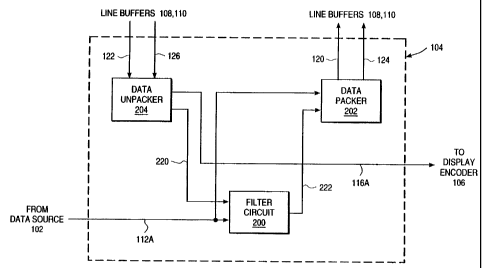
Figure ? is a block diagram of a preferred embodiment of the flicker filter
device 104 of
Fi(yure 1, used to illustrate data flow through the device. The flicker filter
device 104 includes a
filter circuit 200, a data packer 202, and a data unpacker 204. All of the
lines shown in Figure 2
are data lines.
The filter circuit 200 has two inputs and one output. A first input is adapted
to receive
input data in an external format on line 112A; the second input is coupled to
receive data from
the data unpacker 204 on line 220. The output is coupled to send data to the
data packer 202 on
line 222. The filter circuit 200 combines the two input data streams, each of
which typically
represents a line of computer graphics, into a single filtered data line which
is output to the data
packer 202. In a preferred embodiment, the filter circuit 200 forms a weighted
sum of the two
input lines. In other words, each of the input lines is multiplied by a
constant and the two
products then summed to form the filtered line. In other embodiments, the
filter circuit 200 may
combine more than two data streams into a single filtered data line and/or may
receive more
than one data stream on either line l 12A or 220. For example, the filter
circuit 200 may use a
standard filter such as where the first line is multiplied by f and the second
line is multiplied by
( l-f), where 0< f< 1. Still more particularly, such an exemplary filter is
given by a using a pixel
from row 1(Row 1) and a pixel from row 2 (Row 2) in the equation:
(Row t * }) + (Row 2 * (1 - f))
16 16
In this example, the pixels are each 8 bits while f is 4 bits. Each numerator
is therefore
12 bits. Dividing by 16 reduces the result to 8 bits.
The data packer 202 is adapted to write data lines to the line buffers 108 and
110 via
lines 120 and 124. The data packer 202 receives the filtered line from the
filter circuit 200,
converts the filtered line from its external format to an internal format, and
then writes the line
to one of the line buffers 108 or 110.
The terms "internal" and "externalõ are with respect to the line buffers 108
and 110. The
"internal format" is the format used in storing data to the line buffers 108
and 110; while the
"external format" is the one used in processina data in the filter circuit
200.
In a preferred embodiment, the "external format" is the 4:4:4 signed YCrCb
format;
while the "internal format" may be either the 4:2:2 or the 4:1:1 YCrCb format.
The YCrCb
format is advantaoeous because many filters rely heavily on the luminance
value, which is the Y
in YCrCb. The 4:2:2 and 4: 1:1 formats are shorter than the 4:4:4 format, thus
allowina the use
of smaller line buffers 108 and 110 or, alternatively, allowinc, more complex
filtering to be
accomplished with the same size line buffers. For example.data that requires
24 bits per pixel
5
CA 02309605 2000-05-04
WO 99/26229 PCT/US98/24091
(bpp) in 4:4:4 format would require 16 bpp in 4:2:2 format and 12 bpp in 4:1:1
format. The
conversion of the data by the data packer 202 from 4:4:4 YCrCb format to 4:2:2
or 4: 1:1 YCrCb
format may be done using any one of several circuits and methods well know in
the art.
The data unpacker 204 is adapted to read data lines from the line buffers
108,110 via
lines 122, 126, respectively. The data unpacker 204 receives the data line
from the line buffer
106 or 110, converts the line from internal to external format, and then
either sends the line to
the filter circuit 200 for further f4 Itering or outputs the data line on line
116A. The data
unpacker 204 converts the data from 4:2:2 or 4:1:1 YCrCb format to 4:4:4 YCrCb
format using
any one of the conventional circuits or methods well known in the art.
General operation of the flicker filter device 104 occurs as follows. The line
buffers 108
and/or 110 hold intermediate results. The data unpacker 204 reads these
intermediate results
from the line buffers 108 and 110. If the intermediate result is a completed
interlaced line, then
it is output on line 116A. if it is not a completed interlaced line, then the
filter circuit 200
combines the intermediate results with an incoming non-interlaced line
received on line 112A.
The new intermediate result is then written to the line buffers 108 and 110 by
data packer 202,
and the process is repeated.
In an alternate embodiment, the data packer 202 is also adapted to receive
input data in
an external format on line I 12A, thus allowing the writing of such data
directly to the line
buffers 108 and 1 10 without first requiring a pass through the filter circuit
200.
Figure 3A is a detailed block diagram of a preferred embodiment of the flicker
filter
device 104 of FIGS. 1 and 2. In addition to the components shown in Figure 2,
the flicker filter
device 104 further includes a line buffer write control circuit 302, a line
buffer read control
circuit 304, an input register 306, a color space converter 308, an output
control circuit 310, and
clock circuit 312. Before describing how the various components are coupled,
it will be useful
to describe the various signals received and sent by the flicker filter device
104.
The input data on line 112 includes 24 bits of RGB data, denoted by FID(23:01.
The input control signal on line 114 includes control signals for controlling
operation of
the flicker filter device 104 and control signals for controlling display of
the input data. The
former include the signals shown in Table 1 below; while the latter are
denoted by "Controls" in
Figure 3A and are summarized in Table 2.
6
CA 02309605 2000-05-04
WO 99/26229 PCTIUS98/24091
Table 1: Input Control Signals for Controlling the Flicker Filter
Device 104
Input Control Signal Function
SR70[3:2] Determines the internal format.
SR80-88 [8:0]; SR72[6] Controls and coefficients for the color space
converter 308.
SR70 [5,1 ]; SR71-SR77 Controls the filter circuit 200.
SR70 [4] - Controls the output control circuit 310.
CR3D [0] Enables the flicker filter device 104.
SR70[0] Enables flicker filtering.
Table 2: Input Control Signals for Controlling Display of Input
Data
Input Control Signal Function
FIDCLK Dot Clock
FIHSYNC Horizontal Sync
FIVSYNC Vertical Sync
FIHDE Horizontal Display Enable
FIVDE Vertical Display Enable
FIODDF Indicates whether odd field or even field is to
be produced.
FOSSDE Indicates the location of secondary stream data
FIHBLANK Horizontal Blanking
FIVBLANK Vertical Blanking
The output data on line 116 includes 24 bits of 4:4:4 YCrCb data, denoted by
FOD
[23: 0].
The output control signal on line 1 l8 includes the signals shown in Table 3
below.
Table 3: Output Control Signals
OutDut Control Siqnal Function
FODCLK Dot Clock
FCHSYNC Horizontal Sync
7
CA 02309605 2000-05-04
WO 99/26229 PCT/US98/24091
FOVSYNC Vertical Sync
The line buffers 108 and 1 10 can store 720 16-bit pixels or 900 12-bit pixels
in the
preferred embodiment of Figure 3A. Data is written to or read from the line
buffers 108 and 110
in 128 bit chunks, as denoted by signals LBIDW [ 127:0] LBIDR [ 127:0], LB2DW
[ 127:0], and
LB2DR [ 127:0].
Line buffer 108 includes two read pointers and one write pointer. The control
signal for
line buffer 108 on line 128 includes the signals shown in Table 4 below.
Table 4: Control Signals for Line Buffer 108
Control Signal Function
LBLRD Read pulse for first read pointer
LB1RD I Read pulse for second read point
LBLWR Write pulse
LBIRDSEL Selects between first and second read pointers
LBLRST Reset first read pointer and write pointer.
LB 1 RST 1 Reset second read pointer.
Line buffer 110 includes one read pointer and one write pointer. The control
signal for
line buffer 110 on line 130 includes LB2RD, a read pulse; LB2WR, a write
pulse; and LB2RST,
a reset for the read and write pointers.
The couplings and basic functions of each of the components in the flicker
filter device
104 will now be described.
The clock circuit 312 is adapted to receive the input clock FIDCLK and various
other
input control signals on line 114 and outputs two clocks: FICLK and FFCLK.
More
specifically, FIDCLK is inverted and then gated with CR3D[01 (circuit enable),
and SR70(0]
(flicker filter enable), to generate FICLK, which latches input data and input
control signals into
the input register 306 and also clocks the color space converter 308. In turn,
FICLK is inverted
and gated with SR70[01 to generate FFCLK, which clocks the rest of the flicker
filter device
104. The skew from FIDCLK to FICLK and the skew from FICLK to FFCLK each is
preferably
less than half of the minimum clock period.
The input register 306 is adapted to receive the input data on line 112 and
Controls on
line 114. and is also coupled to receive clock FICLK from the clock circuit
312. The register
8
CA 02309605 2000-05-04
WO 99/26229 PCT/US98/24091
306 latches the input data and input control signals on the rising edge of
FICLK and then
outputs the latched controls and RGB data. now denoted as FFD[23:0].
The color space converter 308 is coupled to receive Controls and RGB data
FFD[23:0]
from input register 306 and is also coupled to receive FICLK from the clock
circuit 312 for
clocking purposes. The color space converter 308 is also adapted to receive
various other input
control signale on line 114. The color space converter 308 performs initial
color processing on
the input data, partially in response to the control signals received on line
114. More
specifically, the color space converter 308 converts the input data from RGE
format to 4:4:4
signed YCrCb format, the external format. The color space converter 308 may
also perform
other initial processing, such as color adjustments or chroma filtering. In a
preferred
embodiment, the color space converter 308 includes a 9-tap chroma filter (not
shown) that
performs chroma filtering on the output from the color spaced converter.
Preferably, the chroma
filter uses coefficients of (3, 6, 8, 10, 10, 10, 8, 6, 31, and scales by
1/64. The processed data,
now in YCrCb format, is output on line 112A. The corresponding controls are
also output by
the color space converter 308.
The filter circuit 200 is coupled to receive Controls and the YCrCb data from
the color
space converter 308. the filter circuit 200 is also coupled to receive data
from the data unpacker
204 on line 220. The filter circuit 200 is further coupled to receive FFCLK
from the clock
circuit 312 on line 115 and adapted to receive various input control signals
SR70[5,1] and
SR71-SR77 on line 114. As described previously, the filter circuit 200
combines the received
input data streams into a single filtered data line which is output to the
data packer 202 on line
222. Although Figure 3A only depicts two lines II 2A and 220 for receiving
data to be filtered,
this depiction is for purposes of clarity in Figure 3A. The filter circuit 200
is not limited to
combining two data streams at a time. The filtering is controlled by the
various received control
signals and clocked by FFCLK.
The data packer 202 is coupled to receive the filtered data from the filter
circuit 200 on
line 222. The data packer 202 is also coupled to receive data in the external
format, 4:4:4
YCrCb format in this embodiment, directly from the color space converter 308
on line 112A.
The data packer 202 is further coupled to receive control signals from the
write control circuit
302, adapted to receive input control signals on line 114, and coupled to
receive FFCLK from
the clock circuit 312. As described previously, the data packer 202 converts
received data lines
from the external format to an internal format, and then writes the re-
formatted line to one of the
line buffers 108 or 110 via lines 120 or 124.
9
CA 02309605 2000-05-04
WO 99/26229 PCT/US98/24091
The line buffer write control circuit 302 controls the writinQ of data from
the data packer
202 to the line buffers 108 or 110. More specifically, the write control
circuit 302 is coupled to
receive Controls from the color space converter 308 and FFCLK from the clock
circuit 312, and
is adapted to receive input control signals on line 114. In response to these
inputs,
the write control circuit 302 generates control signals for the data oacker
202 and write control
signals for line buffers 108 and 110 on lines 128 and 130, respectively.
The data unpacker 204 is adapted to receive data lines from the line buffers
108 and 110
via lines 122 and 126. The data unpacker 204 is further coupled to receive
control signals from
the read control circuit 304 and adapted to receive input control signals on
line 114. As
described previously, the data unpacker 204 converts received lines from
internal to external
format, and then either sends the line to the filter circuit 200 on line 220
for further filtering or
outputs the data line on line 116A.
The line buffer read control circuit 306 controls the reading of data from the
line buffers
108 or 110 to the data unpacker 204. More specifically, the read control
circuit 304 is coupled
to receive Controls from the color space converter 308 and FFCLK from the
clock circuit 312,
and is adapted to receive input control signals on line 114. In response to
these inputs, the read
control circuit 304 generates control signals for the data unpacker 204 and
read control signals
for line buffers 108 and 110 on lines 128 and 130, respectively.
Finally, the output control circuit 310 is coupled to receive data from the
data unpacker
204 on line 116A or from the color space converter 308 on line 1 i2A. The
output control
circuit 310 also is coupled to receive control signals from the color space
converter 308, coupled
to receive FICLK and FFCLK from the clock circuit 312, and adapted to receive
input control
signals on line 114. The output control circuit 310 sends output data, denoted
FOD [23:0], to
the display encoder 106 of Figure I on line 116. The output control circuit
310 also converts the
input Controls to output control signals appropriate for the output data. The
output control
signals are transmitted to the display encoder 106 on line 118.
The above components were described in the context of converting non-
interlaced input
data to interlaced output data. The flicker filter device 104, however, need
not always
implement flicker filtering. For example, the flicker filter device 104 may
only perform
conversion of the data from non-interlaced to interlaced without flicker
filtering by setting the
value of f to one. For example, flicker filtering may be disabled by not
asserting SR70C[0]
independent of whether conversion is done. Then, the output data provided by
the output
control circuit 3 10 will be the unfiltered data received from the color space
converter 308 on
CA 02309605 2007-03-19
line 112A. and the output clock FODCLK will be FICLK. In contrast, if flicker
filtering is
enabled, then the output data will be data from the data unpacker 204 on line
I 16A and the
output clock FODCLK will be FFCLK.
Referring now to Figure 3B, a second embodiment 360 of the flicker filter
device 104 is
shown. The second embodiment 360 preferably comprises a color space converter
350, a 9-tap
chroma filter 352, a plurality of multiplexers 356, 358, a filter and aperture
correction circuitry
354, and, other control circuitry 370, 372, 374, 376, 378. The second
embodiment 360 of the
flicker filter device 104 is shown coupled to a plurality of data packers
202a, 202b, a plurality of
data unpackers 204a, 204b, 204c, the first line buffer 108 and the second line
buffer 110.
The color space convener 350 is coupled to the data source 102 to receive an
RGB
signal. The color space converter 350 preferably converts 24 bits of RGB to 24
bits in YCrCb
format. This conversion is done in a conventional manner. The output of the
color space
converter 350 is coupled to the input of the 9tap chroma filter 352. The 9-tap
chroma filter 352
performs chroma filtering in a manner described above using the coefficients
uses coefficients
of (3, 6, 8, 10, 10, 10, 8, 6, 3}, and scaling by 1/64, for example. The
output of the 9-tap
chroma filter 352 is provided to an input of the first multiplexer 356, to an
input of'the second
multiplexer 358, to an input of the flicker filter & aperture correction
circuitry 354, and to an
input of the second data packer 202b.
The second multiplexer 358 also has a second input coupled to the output of
the data
unpacker out 204. The control input is coupled to receive a TVFF enable
signal. Thus, the
second multiplexer 358 either outputs a flicker filtered signal from the data
unpacker out 204 or
an signal that is not flicker filtered directly from the output of the 9-tap
chroma filter 352.
The first multiplexer 356 has its first input coupled to the output of the 9-
tap chroma
filter 352, as described above, and a second output coupled to the output of
the flicker filter
aperture cotrection circuitry 354. The first multiplexer 356 provides at its
output either the new
in coming data line or data from the flicker filter & aperture correction
circuitry 354. The
output of the first multiplexer 356 is in turn coupled to the first data
packer 202a which packs
the data for storage in the first line buffer 108. The first data packer 202a
operates similar to
device 202 described above. The first data packer has an input coupled to the
output of the first
multiplexer 356 and an output coupled to an input of the first line buffer
108.
The first line buffer 108 is used to store data that has been partially
flicker filtered, and
partial sums. The output of the first line buffer 108 is coupled to an input
of the data unpacker
out 204a to send data to the TV encoder 106. The output of the first line
buffer 108 is also
' i~
CA 02309605 2000-05-04
WO 99/26229 PCT/US98/24091
coupled to an input of the data unpacker 1 204a to send data to the flicker
filter aperture
correction circuitry 354.
The data packer 2 202b, the second line buffer 110, and the data unpacker 2
204c are
coupled together like their counter parts the data packer 1 202a, the first
line buffer 108, and the
data unpacker 1 204b. However, the input to the data packer 2 202b is coupled
to the output of
the 9-tap chroma filter 352 as noted above, and the output of the data
unpacker 2 204c is
coupled to a different output of the flicker filter & aperture correction
circuitry 354.
Finally, the second embodiment 360 provides similar control logic including a
line
buffer (LB) write control unit 370, a LB read control unit 372, a clock
generator 374 which is a
division circuit for generating the FODCLK signal, a horizontal sync control
unit 376, and a
vertical sync control unit 378. Based on the timing diagrams that will be
described, those
skilled in the art will understand how to construct these control units and
how they operated to
control the other components shown in Figure 3B.
FIGS. 4-8 illustrate various methods of operating the flicker filter device
104 of
Figure 3A. FIGS. 4-7 illustrate production of interlaced output data from non-
interlaced input
data; while Figure 8 illustrates the production of output control signals from
input control
signals.
Figures 4A and 4B are timins diagram illustrating a method for 2-tap flicker
filtering
utilizina the flicker filter device 104 of Figure 3A. Figure 4A illustrates
the production of an
even field of an interlaced output which displays a total of 4801ines; while
Figure 4B illustrates
the production of the corresponding odd field. The method is not limited to
displays of 480
lines. Line buffer 110 is not required for 2-tap filtering.
The nomenciature used in FIGS. 4A and 4B is as follows. The signals FIODDF,
FIVSYNC.... FOVSYNC are as described previously with respect to Figure 3A. The
nomenclature "Ln't represents input data line n. Thus, in the 480-line example
of FIGS. 4A and
4B, one frame of non-interlaced input data is represented by LO, LI .... L479,
as illustrated in
the row corresponding to FID[23:0]. The nomenclature "Lm, n'l represents the
data line which
results from filtering input data lines m and n together. The output data
lines are LO, 1; L2,
3:..... L478, 479 for the even field of Figure 4A and Li, 2; L3, 4;..... L477,
478; L4791 for the
odd field of Figure 4B, as illustrated in the rows corresponding to FOD [23:
0].
Figure 4A illustrates production of the even field. Line 0 (LO) is received
400 by the
flicker filter device 104 and written 402 to line buffer 108. When line l(LI)
is received 404,
line 0 is read 406 from line buffer 108 and then filtered with line 1. The
filtered line LO, 1 is
12
CA 02309605 2000-05-04
WO 99/26229 PCT/US98/24091
written 408 back to line buffer 108. This is basically a read-modify-write
operation for line
buffer 108. When the filtered data LO, I is written 408 to line buffer 108, it
is read 410 from
line buffer 108 and outputted 412 at half the clock rate at which input data
is received. The
same process is repeated for successive lines to produce the even field.
In more detail, referring additionally to Figure 3A, line 0 is received 400 by
the input
register 306, converted to the externa14:4:4 YCrCb format by the color space
converter 308, and
then converted from the external format to the internal format and written 402
to line buffer 108
by the data packer 202 under control of the write control circuit 302. Line l
is then received 404
by the input register 306 and converted to external format by the color space
converter 308.
Simultaneously, line 0 is read 406 from buffer 108 and converted to external
format by the data
unpacker 204 under control of the read control circuit 304. Lines 0 and 1,
both in external
format, are then combined into filtered line LOJ by filter circuit 200. The
filtered line LO,1 is
converted to internal format and written 408 back to line buffer 108 by the
data packer 202
under control of the write control circuit 302. The data unpacker 204 under
control of the read
control circuit 304 reads 410 the filtered data LO,1 from line buffer 108,
converts it to external
format, and outputs 412 the filtered line LD,I via the output control circuit
310.
One type of write 408 operation is performed to line buffer 108 but two
different types of
read operations are performed: one to read 406 the previously stored line and
one to read 410 the
output line. The two read operations 406, 410 may be implemented by using a
line buffer 108
with two read ports. In the preferred embodiment of Figure 3A, however, the
two read
operations 406, 410 are time multiplexed using two read pointers LBLRD and
LB1RD1, with
signal LBLRDSEL selecting which read pointer is active. As a result, the line
buffer 108 only
requires a single read port.
Furthermore, the first read pointer LBLRD and the write pointer LBLWR are both
reset
by LBLRST, which in this embodiment is generated in response to either FIHSYNC
or the
rising edge of FIHDE. The second read pointer LB1RD1 has an independent reset
LBIRSTI,
which in this embodiment is generated once for every two input lines because
one output data
line is generated for every two input data lines. Since the reset signal
LBLRST is sometimes
generated when LBIRDI is still actively reading from line buffer 108, the
reset LBLRST should
not corrupt data in the line buffer 108.,
In the remaining descriptions, the level of detail contained in the previous
three
paragraphs will be omitted for clarity.
13
CA 02309605 2000-05-04
WO 99/26229 PCT/US98/24091
The odd field of Figure 4B is produced in an analogous manner with the
following
special cases at the beginning and end of the field. At the beginning of the
field, line 0 (LO) is
not used. At the end of the field, the last interlaced output line (L479 1)
should be produced by
filtering lines 479 and 480, but line 480 does not exist. Hence, L4791 is
produced either by not
filterina line 479 or by filtering line 479 with itself. other approaches for
handling these special
cases will be apparent to those of ordinary skill in the art depending on
implementation.
Figures 5A and 5B are timing diagrams illustrating a method for 3-tap flicker
filtering
utilizing the flicker filter device 104 of Figure 3A. As with FIGS. 4A and 4B,
Figure 5A
illustrates the production of an even field of an interlaced format displaying
480 lines; while
Figure 5B illustrates the production of the corresponding odd field.
Basic operation is illustrated by the production of filtered line LO,1,2 in
Figure 5B.
When line 0 (LO) is received 500, it is written 502 to line buffer 110. When
line 1(Li) is
received 504, it is written 506 to line buffer 108. When line 2(L2) is
received 508, LO is read
510 from line buffer 1 10 and Li is read S 12 from line buffer 108. All three
lines LO, Li, and L2
are filtered together and the resulting filtered line LO,1,2 is then written
514 back into line
buffer 108. When the filtered data LO,1,2 is written 514 to line buffer 108,
it is then read 516
from line buffer 108 and outputted 518 at half the input clock rate. Line 2 is
also written 520 to
line buffer 110 in preparation for the production of filtered line L2,3,4. The
same process is
repeated for successive lines.
The read pointer LB2RC and write pointer LB2WR are cleared by L32RST, which in
this embodiment is Generated in response to either FIHSYNC or the rising edge
of FIHDE.
Special cases may occur at the beginning and end of each Alield. For example,
for the
even field of Figure 5A, filtered line LO,1 is a special case since line -1
does not exist. As
another example, for the odd field of Figure SE, filtered line L478,479 is a
special case since
line 480 does not exist. As described previously, various approaches are
generally known for
handling these special cases.
FIGS. 6A and 6B are timing diagrams illustrating a second method for 3-tap
flicker
filtering utilizing the flicker filter device 104 of Figure 3A. As usual,
Figure 6A shows
production of the even field; while Figure 6B shows production of the odd
field.
Basic operation is illustrated by the production of filtered line LO, 1,2 in
Figure 6B.
Line 0 (LO) is received 600 and written 602 to line buffer 110. When line
1(LI) is received
604, line 0 is read 606 from line buffer 110 and filtered with line 1. The
resulting filtered line
14
CA 02309605 2000-05-04
WO 99/26229 PCT/US98/24091
Lo,l, which is an intermediate result, is written 608 to line buffer 108. When
line 2(L2) is
received 610, intermediate result LO,I is read 612 from line buffer 108 and
filtered with line 2.
The filtered line LO,1,2 is then written 614 back to line buffer 108. When the
filtered data
LO,1,2 is written 614 to line buffer 108, it is then read 616 from line buffer
108 and outputted
618 at half the input clock rate. Line 2 is also written 620 to line buffer
110 in preparation for
the production of filtered line L2,3,4. The same process is repeated for
successive lines.
Again, special cases may occur at the beginning and/or end of each field.
Examples
include filtered line LO,1 in Figure 6A and filtered line L478,479 in Figure
6B.
FIGS. 7A and 7B are timing diagrams illustrating a third method for 3-tap
flicker
filtering utilizing the flicker filter device 104 of Figure 3A. As usual,
Figure 7A shows
production of the even field; while Figure 7B shows production of the odd
field.
Basic operation is illustrated by the production of filtered line LO, 1,2 in
Figure 7B.
Line 0 (LO) is received 700 and written 702 to line buffer 108. When line
1(Ll) is received
704, line 0 is read 706 from line buffer 108 and filtered with line 1. The
resulting filtered line
Lo,l, which is an intermediate result, is written 708 to line buffer 108. When
line 2(L2) is
received 710, intermediate result LO,I is read 712 from line buffer 108 and
filtered with line 2.
The filtered line LO,1,2 is then written 714 to line buffer 110. when the
filtered data LO,1,2 is
written 7 14 to line buffer 110, it is then read 716 from line i-:uffer 110
and outputted 718 at half
the input clock rate. Line 2 is also written 720 to line buffer 108 in
preparation for the
production of filtered line L2,3,4. The same process is repeated for
successive lines. Again,
special cases may occur at the beginning and/or end of each field. This method
has an
advantage of not requiring the second read pointer LB1RD 1 for line buffer
108.
The flicker filter device 104 of Figure 3A may implement any of the 2-tap or 3-
tap
flicker filtering methods illustrated above. Hence, one advantage of the
flicker filter device 104
of Figure 3A is that the same hardware may be used to implement different
flicker filter
functions with different numbers of taps.
FIGURE 8 is a timing diagram illustrating the production of output control
signals from
input control signals, utilizing the flicker filter device 104 of FIGURE 3.
More specifically, the
output control circuit 310 generates the interlaced output control signals
FOHSYNC, PODE,
and FOVSYNC from the noninterlaced mode input control signals FIHSYNC, FIHDE,
FIVDE,
FIVBLANK, and FIVSYNC. As a result of the conversion from noninterlaced format
to
interlaced format, input data is received at twice the rate at which output
data is generated.
CA 02309605 2000-05-04
WO 99/26229 PCT/US98/24091
In the preferred embodiment of Figure 8, the generation of output control
signals is
initiated at the beginning of the even field. Figure 8 depicts a time period
corresponding to this
initiation.
FOHSYNC is generated as follows. The portion of the output control circuit 310
that
generates FOHYSNC is reset at the first rising edge 800 of horizontal display
enable (FIHDE)
that follows the falling edge 802 of vertical blank (FIVBLANK) during even
field (i.e., FIODDF
is low 804). Reset does not occur during odd fields. The output control
circuit 310 determines
the start position TI of FIHSYNC, which is the time between the rising edge
800 of FIHDE and
the rising edge 806 of FIHSYNC. The output control circuit 310 also determines
the width T2
of FIHSYNC. Botl, Ti and T2 are multiplied by two to generate the interlaced
horizontal sync
output FOHSYNC, which is referenced to the leading edge 800 of FIHDE. The
flicker filter
data pipeline delay is also added in generation of FOHSYNC. In Figure 8,
Latency is provide to
match the delay through the flicker filter device 200 and the delay in
processing the data in the
color space converter 308.
FODE is aenerated by determining the period T3 from the falling edge 812 of
FIHSYNC
to the next leading edge 814 of FIHDE. The parameters Ti, T2, and T3, are all
multiplied by
two to produce the interlaced output enable FODE, also referenced to the
leading edge 800 of
FIHDE.
In the embodiment of Figure 8, the generation of FOHSYNC and starts one line
earlier
from the first active input line (LO) or two lines earlier from the first
active output data (LO,1)
and output display enable (FODE). This results in the correct synchronization
of FOHSYNC
with FODE and FCD(23:01. In general, generation of FOHSYNC must begin at a
point which
ensures that FOHSYNC will be generated in between two output lines.
FOVSYNC is generated by delaying FIVSYNC by the flicker filter data pipeline
delay
and also by the amount specified in TV VSYNC delay register (SR78). A counter
which is used
to delay both the rising edge and the falling edge of FIVSYNC by the amount
specified by SR78
is incremented by FFCLK/16. Because the vertical sync can be delayed by more
than one
horizontal time, FIVSYNC can be optionally programmed such that it is
generated one line
earlier than shown ;-n the above timing diagrams and then delayed by
approximately one
horizontal time. This is highly recommended because FOVSYNC can then be
positioned
independently of FOHSYNC. The delay depends on timing based on the programming
of -.he
CRT controller.
16
CA 02309605 2000-05-04
WO 99/26229 PCT/US98/24091
Although the invention has been described in considerable detail with
reference to
certain preferred embodiments thereof, other embodiments are possible. For
example, the
invention can be incorporated into an integrated circuit on a semiconductor
device using
techniques known in the art. Therefore, the spirit and scope of the appended
claims should not
be limited to the description of the preferred embodiments contained herein.
17