Note: Descriptions are shown in the official language in which they were submitted.
CA 02309643 2000-OS-09
DESCRIPTION
THERMAL PRINT HEAD
Technical Field
The present invention relates to a thermal print head
composed of a heating board and a radiating plate, detailedly
relates to a thermal print head provided with an identification
to mark for positioning when a heating board is bonded to a radiating
plate.
Background Art
Heretofore, this type of thermal print head is composed
by attaching a ceramic heating board onto the upper surface of
a metallic radiating plate. A heating resistor for printing,
a common electrode pattern and an individual electrode pattern
are formed on the surface of the heating board and plural IC
chips for driving are mounted. In case the heating board having
2o the configuration described above is attached to the radiating
plate, an adhesive and a pressure sensitive adhesive tape are
generally used, however, in any case, precise positioning is
required and particularly, to position precisely in the
longitudinal direction of the heating board, that is, in the
1
CA 02309643 2000-OS-09
direction of the x-axis which is a direction in which the heating
resistor is arranged, heretofore, a first dot part (the leading
end) and a last dot part (the trailing end) of the heating
resistor linearly formed on the heating board are based.
That is, the first dot part and the last dot part of the
heating resistor are directly recognized as a binary number by
a camera and others, the heating board is precisely set on the
radiating plate and is bonded based upon it.
However, recently, the demand of a thermal print head
to wherein a heating resistor is covered with a conductive
protective coat is increased and a problem that precision in
bonding between a heating board and a radiating plate decreases
because such a conductive protective coat is formed occurs.
That is, as a heating resistor is generally black, while
a conductive protective coat is also approximately black, it
is difficult to recognize the first dot part and the last dot
part of the heating resistor by a camera and as a result,
misregistration by wrong recognition occurs.
Therefore, it is considered that an identification mark
different from a heating resistor is required and is based,
however, wrong recognition is caused depending upon the shape
of a mark and satisfactory bonding precision is not achieved.
The object of the invention is to provide a thermal print head
wherein an identification mark for positioning enabling solving
such problems is provided.
2
CA 02309643 2000-OS-09
Disclosure of the Invention
To solve the problems, a first aspect of the invention is
based upon a thermal print head wherein a heating board on the
surface of which a heating resistor for printing is formed is
attached on the upper surface of a radiating plate and is
characterized in that the heating board is provided with an
identification mark having the vertical side for an orientation
to arranged perpendicularly to a direction in which heating
resistor is arranged so that the identification mark functions
as the orientation when the heating board is attached to the
radiating plate.
Therefore, as a first dot part and a last dot part of the
heating resistor can be more definitely recognized than they
are directly recognized as a binary number by a camera,
positioning when the heating board is attached to the radiating
plate can be precisely performed. Particularly, even if the
identification mark is formed using gold foil and others which
2o is hardly recognized when the parts are recognized as a binary
number, a longitudinal reference line formed by the vertical
side definitely appears and wrong recognition can be possibly
prevented.
Also, a second aspect of the invention is based upon the
thermal print head according to the first aspect of the invention
3
CA 02309643 2000-OS-09
and is characterized in that the heating resistor is covered
With a protective coat. That is, as positioning can be precisely
performed even if it is difficult to recognize the heating
resistor as a binary number by a camera because of the protective
coat, positional precision for attaching the heating board onto
the radiating plate can be enhanced.
Also, a third aspect of the invention is based upon the
thermal print head according to the first aspect of the invention
and is characterized the identification mark is provided in a
1o position except the protective coat.
Therefore, even if the identification mark is formed in
approximately the same color as that of the protective coat,
a precise positional reference can be acquired.
Also, a fourth aspect of the invention is based upon the
thermal print head according to the first aspect of the invention
and is characterized in that as for the identification mark,
the vertical side is provided in only one location. Therefore,
there is no possibility that another vertical side is recognized
as a reference position by mistake.
A fifth aspect of the invention is based upon the thermal
print head according to any of the first to third aspects of
the invention and is characterized in that the identification
mark is composed of an X reference line formed by the vertical
side and a Y reference line formed by the side perpendicular
to the vertical side.
4
CA 02309643 2000-OS-09
According to such configuration, alignment not only in the
longitudinal direction (the direction of Xj but in the direction
of Y can be achieved and extremely precise alignment is enabled.
A sixth aspect of the invention is based upon the thermal
print head according to the first aspect of the invention and
is characterized in that the identification mark is made of a
thick film printed pattern.
A seventh aspect of the invention is based upon the thermal
print head according to the first aspect of the invention and
to is characterized in that the identification mark is made of a
thin film pattern.
An eighth aspect of the invention is based upon the thermal
print head according to the sixth or seventh aspect of the
invention and is characterized in that the identification mark
is formed in a process for forming an electrode pattern.
According to such configuration, the identification mark can
be formed at the same time that the electrode pattern is formed
without requiring another process and further, as relative
positioning is applied to the electrode pattern by a mask,
2o extremely precise positioning is enabled.
Also, a ninth aspect of the invention is based upon the
thermal print head according to any of the first to the third
aspects of the invention and is characterized in that the
identification mark is a polygon having the vertical side as
one side. Therefore, in case the polygon is recognized as a
5
CA 02309643 2000-OS-09
binary number, the plane is clearly shown and the vertical side
to be a reference can be definitely recognized. Also, for
example, in the case of a polygon having the side perpendicular
to the vertical side, positioning not only in the longitudinal
direction of the heating board but in the direction of the width
can be precisely performed.
Further, a tenth aspect of the invention is based upon the
thermal print head according to any of the first to third aspects
of the invention and is characterized in that the identification
l0 mark is a semicircle having the vertical side as one side.
Therefore, the area of the mark to acquire precise recognition
can be reduced up to the required minimum limit, the quantity
of pasted gold, aluminum and others for forming the mark can
be reduced and the cost can be reduced.
An eleventh aspect of the invention is based upon a method
of mounting the heating board on the surface of which the heating
resistor for printing is formed on the radiating plate and
forming the thermal print head and is characterized in that a
process for forming the heating board on which the heating
2o resistor for printing, the identification mark having the
vertical side perpendicular to a direction in which the heating
resistor is arranged and the electrode pattern connected to the
heating resistor are formed and a process for aligning and fixing
the heating board on the radiating plate using the vertical side
of the identification mark as a positioning reference line are
6
CA 02309643 2000-OS-09
included. Therefore, as the first dot part and the last dot part
of the heating resistor can be more definitely recognized than
they are directly recognized as a binary number by a camera,
positioning when the heating board is attached on the radiating
plate can be precisely performed. Particularly, a longitudinal
reference line formed by the vertical side to be a reference
is definitely shown and wrong recognition can be possibly
prevented.
A twelfth aspect of the invention is based upon the method
of manufacturing the thermal print head according to the eleventh
aspect of the invention and is characterized in that the
identification mark is formed in the process for forming the
electrode pattern. According to such a method, the
identification mark can be easily formed without requiring
another process.
A thirteenth aspect of the invention is based upon the
method of manufacturing the thermal print head according to the
eleventh aspect of the invention and is characterized in that
the identification mark is composed of an X reference line formed
2o by the vertical side and a Y reference line formed by the side
perpendicular to the vertical side.
A fourteenth aspect of the invention is based upon the
method of manufacturing the thermal print head according to the
eleventh aspect of the invention and is characterized in that
the process for forming the identification mark is equivalent
7
CA 02309643 2000-OS-09
to the process for forming the electrode pattern . According to
such configuration, alignment not only in the longitudinal
direction (the direction of X) but in the direction of Y can
be achieved and extremely precise alignment is enabled.
A fifteenth aspect of the invention is based upon the method
of manufacturing the thermal print head according to the
fourteenth aspect of the invention and is characterized in that
the process for forming the identification mark includes a thick
film printing process.
1 o A sixteenth aspect of the inventi on i s based upon the method
of manufacturing the thermal print head according to the
fourteenth aspect of the invention and is characterized in that
the process for forming the identification mark includes the
thick film printing process for printing on the whole surface
and a pattern forming process for patterning it by
photolithography.
A seventeenth aspect of the invention is based upon the
method of manufacturing the thermal print head according to the
fourteenth aspect of the invention and is characterized in that
2o the process for forming the identification mark includes a thin
film forming process and the pattern forming process for
patterning it by photolithography.
The invention is based upon a thermal print head wherein
a heating board on the surface of which a heating resistor for
printing is formed is attached on the upper surface of a radiating
8
CA 02309643 2000-OS-09
plate and is characterized in that an identification mark which
functions as a positioning reference when a heating board,is
attached on a radiating plate is provided on the heating board
at a fixed interval from a heating resistor and in addition,
the identification mark has the vertical side equivalent to a
positioning reference line in the direction of the x-axis
equivalent to the longitudinal direction of the heating board.
That is, the first dot part and the last dot part of the
1o heating resistor can be more definitely recognized by providing
the identification mark for positioning on the heating board
than they are directly recognized as a binary number by a camera
as heretofore, positioning when the heating board is attached
on the radiating plate can be precisely performed and attaching
precision can be enhanced.
The identification mark can be easily formed by printing
and gold, aluminum and others are suitably used for paste for
printing.
Particularly as for gold, in case it is binarized when it
2o is monitored by a television camera, it is often judged blank,
however, in the case of the shape described above, as a
longitudinal reference line formed by the vertical side to be
a reference is definitely shown, gold paste may be used.
The heating resistor of a thermal print head is often
covered with a conductive protective coat and in the case of
9
CA 02309643 2000-OS-09
such a thermal print head the heating resistor of which is covered
with a conductive protective coat and in addition, in case the
color of the heating resistor is approximately the same color
as that of the protective coat, it is difficult to directly
recognize the first dot part and the last dot part of the heating
resistor as a binary number by a monitor as described above,
however, positioning can be precisely performed by providing
the identification mark at a fixed interval from the heating
resistor.
l0 Such an identification mark can be also formed on the
conductive protective coat, however, even if the identification
mark is formed in approximately the same color as that of the
protective coat, a precise positional reference can be acquired
by providing the identification mark in a position in which no
protective coat is provided.
The identification mark can be in a shape such as the
vertical side is provided in only one location. The reason is
that when plural vertical lines to be a reference are provided,
they are misleading and other vertical lines are easily wrongly
2o recognized as a reference position.
Also, the identification mark may be also a polygon and
a semicircle each one side of which is a vertical side.
As these shapes are familiar and a plane is clearly shown
in case they are binarized, the vertical side to be a reference
can be definitely recognized.
CA 02309643 2000-OS-09
Particularly, in the case of a polygon having the side
perpendicular to the vertical side, positioning not only in the
longitudinal direction of the heating board but in the direction
of the width can be precisely performed.
Further, in the case of a triangle, paste such as gold and
aluminum for forming the identification mark is saved and the
cost can be reduced.
To reduce the quantity of paste, as the area can be minimized
in the case of a semicircle, it is more effective to reduce the
l0 cost.
Brief Description of the Drawings
Fig. 1 is a plan showing a thermal print head equivalent
to an embodiment;
Fig. 2 is an exploded perspective view showing the thermal
print head;
Fig. 3 is an explanatory drawing showing an embodiment of
an identification mark;
2o Fig. 4 is an explanatory drawing showing another embodiment
of the identification mark;
Fig. 5 is an explanatory drawing showing further another
embodiment of the identification mark;
Fig. 6 is an explanatory drawing showing further another
embodiment of the identification mark;
11
CA 02309643 2000-OS-09
Fig. 7 is an explanatory drawing showing further another
embodiment of the identification mark; and
Fig. 8 is an explanatory drawing showing the other
embodiment of the identification mark.
Best Mode for Carrying Out the Invention
Referring to the drawings , an embodiment of the invention
will be described in detail below.
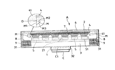
to Fig. 1 is a plan showing a thermal print head A equivalent
to this embodiment and Fig. 2 is an exploded perspective view
showing the thermal print head A.
As shown in these drawings, the thermal print head A is
characterized in that a ceramic heating board 2 and a printed
circuit board 3 made of synthetic resin are aligned and fixed
on the upper surface of a radiation plate 1 made of metal such
as aluminum using an alignment mark M having a positioning
reference line perpendicular to the longitudinal direction of
the heating board 2 . The alignment mark M is formed in a process
2o for forming a common electrode pattern 6 or an individual
electrode pattern 7.
The upper surface of the radiating plate 1 is composed of
upper and lower planes for mounting the boards 11 and 12 as shown
in Fig. 2, the heating board 2 is mounted on the higher plane
11 and the printed circuit board 3 is mounted on the lower plane
12
CA 02309643 2000-OS-09
12 . In this embodiment, the boards are bonded using a W adhesive .
In Fig. 2, the common electrode pattern 6, the individual
electrode pattern 7 and IC for driving 5 are omitted.
The heating resistor for printing 4 is formed near one side
in the longitudinal direction of the surface of the heating board
2 on the heating board 2 with the resistor linearly extended
and plural IC chips for driving 5 are arranged in a row near
a side opposite to the side described above. The heating
resistor 4 made of ruthenium oxide (Ru02) and formed linearly
to by thick film printing, the common electrode pattern 6 and the
individual electrode pattern 7 are formed on the heating board
2. These common electrode pattern 6 and individual electrode
pattern 7 are made of a gold thick film pattern formed alternately
like a comb so that they are opposite from a direction
perpendicular to the heating resistor under the heating resistor.
The other end of the individual electrode pattern 7 is connected
to the IC chip for driving 5. Also, the common electrode pattern
6 is composed of the side extended in the longitudinal direction
of the heating board 2 , an extended part extended along a shorter
2o side on both sides of the side and connected to the printed
circuit board 3 and a comb-type electrode part forming the teeth
of a comb vertically extended from the side to the heating
resistor 4 and the comb-type electrode part is connected to the
heating resistor. The extended part is connected to the printed
circuit board 3 via a terminal electrode 8 and a terminal lead
13
CA 02309643 2000-OS-09
9 provided at both ends of the printed circuit board 3. The
heating resistor 4 is covered with a conductive protective coat
41 having predetermined width. The conductive protective coat
41 is formed to prevent destruction by static electricity. The
common electrode pattern and the individual electrode pattern
are formed by patterning a gold film formed on the whole surface
of the board by thick film printing using photolithography and
the alignment mark M can be easily formed only by changing a
mask used for the photolithography without requiring a special
to process. Also, it is desirable that the alignment mark has a
vertical side M1 perpendicular to the longitudinal direction
in which a minute and high-precision pattern can be formed
because the alignment mark is formed by photolithography and
a parallel side M2 perpendicular to the vertical side, a position
in the longitudinal direction , that is, the direction of the
x-axis and in the direction of the y-axis perpendicular to the
direction of the x-axis is precisely defined and precise
alignment is enabled by positioning based upon the alignment
mark.
2o Each terminal electrode 8 connected to each IC chip for
driving 5 via a wiring pattern not shown is formed at both ends
of a longer side of the IC chip for driving 5, and each terminal
electrode 8 and a connecting electrode 31 formed at right and
left ends on the upper surface of the printed circuit board 3
are connected via the terminal lead 9.
14
CA 02309643 2000-OS-09
Further, bonding wire not shown connects each individual
electrode pattern 7 and the IC chip for driving 5 and connects
the IC chip for driving 5 and each wiring pattern not shown,
and the IC chip for driving 5 and the bonding wire are covered
with a protective coat 51 made of synthetic resin.
As for the printed circuit board 3, a connector connection
32 is formed approximately in the center of the longer side of
the printed circuit board, and a wiring circuit pattern not shown
for connecting a connector C connected to the connector
to connection 32 for connecting an external device and the
connecting electrode 31 is formed on the surface of the board.
A reference number 21 shown in Fig. 1 denotes a thermistor
arranged between the rows of the IC chip for driving 5 as a
thermostatic element and Cl denotes a contact pin of the
connector C for connecting an external device.
When the thermal print head A is manufactured, a process
for bonding the heating board 2 to the radiating plate 1 is
required, however, in that case, first, the heating board 2 and
the printed circuit board 3 are coupled via the terminal lead
9 and both are simultaneously bonded on the radiating plate 1.
At this time, when the heating board 2 and the printed circuit
board 3 are coupled and when both are bonded on the radiating
plate 1, the heating board 2 is required to be precisely
positioned using the alignment mark M and is required to be
precisely laid on the surface to be mounted.
CA 02309643 2000-OS-09
According to the invention, extremely precise positioning
is enabled, compared with a conventional method of catching the
heating board 2 by a pair of tweezers and others, driving an
XY table, positioning and setting the heating board, recognizing
any mark on the heating board 2, the first dot part and the last
dot part as a mark of the heating resistor 4 as a binary number
by a camera not shown. As described above, the invention is
characterized in that the identification mark M that functions
as a positioning reference in positioning is provided at a fixed
to interval from the heating resistor 4 on the heating board 2 and
in addition, the identification mark M has a vertical side M1
equivalent to a positioning reference line D in the direction
of the x-axis equivalent to the longitudinal direction of the
heating board 2.
In this embodiment, as shown in Fig. 1, the identification
mark M is respectively formed by gold paste by printing at a
predetermined interval on the side of the IC chip for driving
5 respectively from a leading end equivalent to the first dot
part of the heating resistor 4 and from a trailing end equivalent
to the last dot part, and in addition, each identification mark
M is in the shape of a right isosceles triangle composed of the
vertical side M1 equivalent to the positioning reference line
D, a horizontal side M2 perpendicular to the vertical side and
having the same length as the vertical side and a hypotenuse
M3 in this embodiment (see Fig. 3).
16
CA 02309643 2000-OS-09
As described above, a reference can be more definitely
recognized by providing the identification mark M for
positioning than the first dot part and the last dot part of
the heating resistor 4 are directly recognized as a binary number
by a camera as heretofore and positioning when the heating board
2 is attached on the radiating plate 1 can be precisely performed.
In addition, as the heating resistor 4 is not directly
recognized but the identification mark is provided in a position
apart from the heating resistor even if the heating resistor
l0 4 is covered with the conductive protective coat 41 as in this
embodiment, precise positioning is enabled independent of
whether the conductive protective coat 41 is provided or not
and attaching positional precision can be enhanced.
Also, as the mark is in the shape of not a dot and a line
but a plane figure, the vertical side Ml to be a reference line
is definitely shown longitudinally. Therefore, even if the
identification mark M is formed using gold paste often judged
blank when binarized as in this embodiment, wrong recognition
can be prevented.
2o Further, paste for forming the mark having the same color
as that of the conductive protective coat 41 can be used by
forming the identification mark M in a position apart from the
conductive protective coat 41 as shown in Fig. 1 and the degree
of freedom in selecting paste is increased.
Also, in this embodiment, as the vertical side M1 of the
17
CA 02309643 2000-OS-09
identification mark M is provided in only one location, no other
vertical lines that may be recognized as a reference position
by mistake exist, the vertical side can be precisely recognized
and attaching positional precision can be more enhanced.
Further, in this embodiment, as the horizontal side M2
perpendicular to the vertical side Ml is provided, positioning
both in the longitudinal direction of the heating board 2 and
in the direction of the width can be precisely performed.
In addition, the area of the identification mark M can be
to possibly reduced by providing a triangular mark, gold paste is
saved and the cost can be reduced.
Any identification mark M having the vertical side M1
equivalent to the positioning reference line D is included in
the invention and the present invention is not limited to the
identification marks described above. For example, the
identification mark M may be also in the shape of an equilateral
triangle having the vertical side as a base as shown in Fig.
4.
Also, the identification mark may be also a square shown
2o in Fig. 5 or a rectangle for example without limiting to the
triangle. However, in these cases, as a border line M4
equivalent to the vertical side M1 shown in Fig. 3 appears in
parallel, it may be difficult to discriminate which vertical
line is to be a reference.
Further, the identification mark M may be also not only
18
CA 02309643 2000-OS-09
the triangle and the quadrangle but another polygon and for
example, shapes shown in Figs. 6 (a) to 6 (c) are conceivable.
The identification mark M is not a polygon but may be also
a semicircle having the vertical side M1 as one side as shown
in Fig. 7. In this case, the area of the identification mark
M can be reduced up to a required minimum limit and the cost
can be most reduced because the quantity of paste for forming
the mark is saved.
Furthermore, the identification mark M may be also in
to various shape except the shapes described above, for example
shown in Figs. 8 (a) to 8 (f). Any shape shown in Figs. 3 to
8 except Fig. 5 has the vertical side M1 in only one location.
Needless to say, as for the shape of the identification
mark M, further various shapes are conceivable in a range of
the object of the invention. Also, a position in which the
identification mark M is formed is also not limited to the
embodiment, may be suitably determined and for example, may be
also on the conductive protective coat 41.
Also, in the embodiment, the electrode pattern is formed
2o by thick film printing and photolithography, however, a printing
pattern using a mask screen having an electrode pattern and a
pattern of an alignment mark may be also used.
Furthermore, an electrode pattern can be also formed by
patterning a thin film pattern formed by a method such as vacuum
deposition and sputtering by photolithography.
19
CA 02309643 2000-OS-09
Also, in the embodiment, the heating resistor is composed
of an integrated pattern formed linearly and for the electrode,
the comb-type electrode is used, however, it need scarcely be
said that the invention can be also applied to a case that the
heating resistor is formed by an individual pattern.
Furthermore, the alignment mark is not necessarily required to
be formed in the electrode pattern forming process and may be
also formed in another process.
Industrial Applicability
According to the invention, in the thermal print head
composed by attaching the heating board on the surface of which
the heating resistor for printing is formed on the upper surface
of the radiating plate, the identification mark to be a
positioning reference when the heating board is attached on the
radiating plate is provided at a fixed interval from the heating
resistor on the heating board, in addition, the longitudinal
reference line formed by the vertical side to be reference is
2o definitely shown by providing a vertical side equivalent to a
positioning reference line in the direction of the x-axis
equivalent to the longitudinal direction of the heating board
to the identification mark and wrong recognition can be possibly
prevented, and positioning when the heating board is attached
on the radiating plate can be precisely performed.
CA 02309643 2000-OS-09
According to the invention, in the thermal print head, even
if the heating resistor is covered with the protective coat,
positional precision in attaching the heating board on the
radiating plate can be enhanced as in the case described above .
According to the invention, as the identification mark is
provided in a position apart from the protective coat, a precise
positional reference can be acquired even if the identification
mark is formed in approximately the same color as that of the
protective coat and the degree of freedom in selecting the type
to of paste for forming the mark is increased.
According to the invention, as the identification mark has
the vertical side in only one location, no other vertical sides
are recognized as a reference position by mistake.
According to the invention, as the identification mark is
a polygon having a vertical side as one side, a plane is clearly
shown when binarized and the vertical side to be a reference
can be definitely recognized. Also, in case the identification
mark is a polygon having a bottom perpendicular to the vertical
side, positioning not only in the longitudinal direction of the
2o heating board but in the direction of the width can be precisely
performed.
According to the invention, as the identification mark is
a semicircle having a vertical side as one side, the area of
the mark for acquiring precise recognition can be reduced up
to a required minimum limit, the quantity of paste such as gold
21
CA 02309643 2000-OS-09
and aluminum for forming the mark can be reduced and the cost
can be reduced.