Note: Descriptions are shown in the official language in which they were submitted.
CA 02309911 2000-05-12
WO 99/26226 PCT/US98/24216
SPECIFICATION
SYSTEM AND METHOD FOR REDUCING PEAK CURRENT AND
BSANDWIDTH REQUIREMENTS IN A DISPLAY DRIVER CIRCUIT
BACKGROUND OF THE INVENTION
Field of the Invention
This invention relates generally to circuits for driving electronic displays,
and more
particularly to a system and method for using an intemal sequencer to
sequentially drive the
select lines of a display.
Descrintion of the Background Art
FIG. 1 shows a prior art display driver circuit 100, for driving a display 102
which
includes an array of pixel cells arranged in 768 rows and 1024 columns.
Display driver circuit
100 includes select decoder 104, row decoder 106, write hold register 108,
pointer 110,
instruction decoder 112, invert logic 114, timing generator 116, and input
buffers 118, 120, and
122. Driver circuit 100 receives clock signals via an SCLK terminal 124,
invert signals via an
invert (INV) terminal 126, data and addresses via a 32-bit system data bus
128, and operating
instructions via a 3-bit op-code bus 130, all from a system (e.g., a computer)
not shown. Timing
generator 116 generates timing signals, by methods well known to those skilled
in the art, and
provides these timing signals to the components of driver circuit 100 via
clock signal lines (not
shown) to coordinate the operation of the various components.
Invert logic 114 receives the invert signals from the system via INV terminal
126 and
buffer 118, and receives the data and addresses from the system via system
data bus 128 and
buffer 120. Responsive to a first invert signal ( INV ), invert logic 114
asserts the received data
and addresses on a 32-bit intemal data bus 132. Responsive to a second invert
signal (INV),
1
CA 02309911 2000-05-12
WO 99/26226 PCT/US98/24216
invert logic asserts the complement of the received data on intennal data bus
'132. Internal data
bus 132 provides the asserted data to write hold register 108, and provides
the asserted addresses
to select decoder 104, via 5 of the 321ines, and to row decoder 106, via 10 of
the 32 lines.
Instruction decoder 112 receives op-code instructions from the system, via op-
code bus
130 and buffer 122, and, responsive to the received instructions; provides
control signals, via an
internal control bus 134, to select decoder 104, row decoder 106, write hold
register 108, and
pointer 110. Responsive to the system asserting data on system data bus 128
and a first
instruction (i.e., Data Write) on op-code bus 130, instruction decoder 112
asserts control signals
on control bus 134, causing write hold register 108 to load the asserted data
via internal data bus
132 into a first portion of write hold register 108. Because internal data bus
132 is only 32 bits
wide, 32 data write commands are necessary to load an entire line (1024 bits)
of data into write
hold register 108. Pointer 1.10 provides an address, via a set of address
lines 135, to write hold
register 108, identifying the portion of write hold register 108 to which data
is to be written. As
each successive Data Write command is executed, pointer 110 increments the
address asserted
on lines 135 to identify the next 32-bit portion of write hold register 108.
Responsive to the system asserting a row address on system data bus 128 and a
second
instruction (i.e., Load Row Address) on op-code bus 130, instruction decoder
112 asserts control
signals on control bus 134 causing row decoder 106 to store the asserted row
address. Then,
responsive to the system asserting a third instruction (i.e., Array Write) on
op-code bus 130,
instruction decoder 112 asserts control signals on control bus 134, causing
write hold register
108 to assert the 1024 bits of stored data on a set of 1024 data output
terminals 136, and causing
row decoder 106 to decode the stored row address and assert a write signal on
one of 768 word-
lines 138 corresponding to the decoded row address. The write signal on the
corresponding
word-line causes the data being asserted on data output terminals 136 to be
latched into a
corresponding row of pixel cells in display 102.
Responsive to the system asserting a block address on system data bus 128 and
a fourth
instruction (i.e., Load Block Address) on op-code bus 130, instruction decoder
112 asserts
control signals on control bus 134, causing select decoder 104 to store the
asserted block
address. Then, responsive to the system asserting a fiffth instruction (i.e.,
Pixel Update) on op-
code bus 130, instruction decoder 112 asserts control signals on control bus
134 causing select
decoder 104 to decode the asserted address and assert a block update signal on
one of a group of
24 block select lines 140 corresponding to the decoded block address. The
block update sig'nal
2
CA 02309911 2006-09-01
on the corresponding block select line causes all of the pixels cells of an
associated block
to assert the previously latched data onto their associated pixel electrodes
(not shown in
FIG. 1).
FIG. 2 shows an exemplary dual-latch pixel cell 200(r,c,b) of display 102,
where (r),
(c), and (b) indicate the row, column, and block of the pixel cell,
respectively. Pixel cell
200 includes a master latch 202, a slave latch 204, a pixel electrode 206, and
switching
transistors 208, 210, and 212. Master latch 202 is a static random access
memory (SRAM)
latch. One input of master latch 202 is coupled, via transistor 208, to a
Bit+data line
214(c), and the other input of master latch 202 is coupled, via transistor
210, to a Bit-data
line 216(c). The gate terminals of transistors 208 and 210 are coupled to word
line 138(r).
The output of master latch 202 is coupled, via transistor 212, to the input of
slave latch
204. The gate terminal of transistor 212 is coupled to block select line
140(b). The output
of slave latch 204 is coupled to pixel electrode 206.
A write signal on word line 138(r) places transistors 208 and 210 into a
conducting
state, causing the complementary data asserted on data lines 214(c) and 216(c)
to be
latched, such that the output of master latch 202 is at the same logic level
as data line
214(c). A block select signal on block select line 140(b) places transistor
212 into a
conducting state, and causes the data being asserted on the output of master
latch 202 to be
latched onto the output of slave latch 204, and thus onto coupled pixel
electrode 206.
FIG. 3 illustrates how display 102 is divided into 24 blocks (0-23), each
containing
32 rows, for purposes of updating the pixel cells. Each block contains 32 rows
of pixel
cells, all coupled to one block select line 140(b). Accordingly, all of the
pixel cells of a
given block are updated simultaneously. The division of a display into blocks
for the
purpose of updating the pixel cells is further described in U.S. Pat. No.
5,278,652, which
issued to Urbanus et al. on Jan. 11, 1994.
FIG. 4 shows the temporal relationship of the pixel updates. During the first
SCLK
cycle, a load address (LA) command loads the address of the first block to be
updated
(Block 0). Then, during the next clock cycle, an update block command (UB)
causes all of
the pixel cells in Block 0 to be updated. This two-step sequence of loading an
address and
updating a block is repeated until each of the blocks in the display are
updated.
FIG. 5 shows the temporal relationship of the row updates within a block. In
particular, note that all rows within a block are updated simultaneously. For
example,
Rows 0-31 of Block 0 are all updated responsive to the first update block
command.
Similarly, Rows 0-31 of Block
3
CA 02309911 2000-05-12
WO 99/26226 PCT/US98/24216
1 are all updated responsive to the second update block command. This is
because all of the
pixels within a block are coupled to a common select line. '
The above described prior art suffers a disadvantage, in that simultaneously
updating all
of the pixels within a block generates a relatively large amount of peak
current. For example,
for blocks having 32 rows of 1024 pixels, 32,768 pixel electrodes must be
charged (or
discharged) at one time. Furthermore, in the prior art, the number of rows in
each block cannot
be substantially decreased, because the decrease would result in an increased
number of blocks,
and an unacceptable system interface bandwidth requirement to perform the
increased number of
block updates.
What is needed, therefore, is a display driver circuit with a reduced peak
current
requirement and a reduced system interface bandwidth requirement.
SUMMARY
A novel display driver circuit is described. The display driver circuit
includes a select
line sequencer, for providing a series of select line addresses at an output,
and a select line
decoder coupled to the output of the select line sequencer, for decoding each
of the select line
addresses and asserting an update signal on a corresponding one of a plurality
of output
terminals. Optionally, the select line sequencer generates a series of select
sub-line addresses,
and the select line decoder is a select sub-line decoder.
Optionally, the display driver circuit includes a select address register
coupled to the
select line sequencer for providing an initial select line address to the
select line sequencer, and
an input terminal for receiving another initial select line address. It should
be understood that
receiving an initial select line address is interpreted to include receiving a
block address and
converting the block address to an initial select line address. The select
line sequencer further
includes a control input terminal for receiving control signals. Responsive to
a first control
signal, the select line sequencer outputs the next address of the series of
select line addresses.
Responsive to a second control signal, the select line sequencer outputs a new
series of select
line addresses starting from the other initial select line address provided by
the select address
register.
In a particular embodiment, the display driver circuit further includes a
select sub-line
sequencer, for providing a series of select sub-line addresses on an address
terminal set, and a
select sub-line decoder coupled to the address terminal set, for decoding each
of the select sub-
4
CA 02309911 2000-05-12
WO 99/26226 PCT/US98/24216
line addresses and asserting an update signal on a corresponding one of a
plurality of output
terminals.
A novel method for updating a display is also disclosed. The method includes
the steps
of receiving a first initial select line address from a system, generating a
series of select line
addresses based on the first initial select line address, decoding each of the
select line addresses
of the series, and asserting a series of update signals on a first group of
output terminals, each
terminal of the first group corresponding to an associated select line
address. Optionally, the
method includes the steps of receiving another initial select line address,
and generating another
series of select line addresses based on the another initial select line
address. Optionally, the
method further includes the steps of generating a series of select sub-line
addresses, decoding
each of the select sub-line addresses of the series, and asserting a series of
update signals on a
second group of output terminals, each terminal of the second group
corresponding to an
associated select sub-line address.
An alternate method includes the steps of receiving a first initial select sub-
line address
from a system, generating a series of select sub-line addresses based on the
first initial select
sub-line address, decoding each of the select sub-line addresses of the
series, and asserting a
series of update signals on a plurality of output terminals, each terminal of
the plurality of output
terminals corresponding to an associated select sub-line address.
It should be understood that receiving an initial select line address is
interpreted to
include receiving a block address and converting the block address to an
initial select line
address. Similarly, it should be understood that receiving an initial select
sub-line address is
interpreted to include receiving a block address and converting the block
address to an initial
select sub-line address.
BRIEF DESCRIPTION OF THE DRAWINGS
The present invention is described with reference to the following drawings,
wherein like
reference numbers denote substantially similar elements:
FIG. 1 is a block diagram of a prior art display driver circuit;
FIG. 2 is a block diagram of a prior art, dual-latched pixel cell;
FIG. 3 illustrates the division of a display into blocks of rows;
FIG. 4 is a timing diagram showing the updating of blocks of pixel cells;
FIG. 5 is a timing diagram showing the updating of rows of pixel cells within
a block;
5
CA 02309911 2006-09-01
FIG. 6 is a block diagram of one embodiment of a display driver circuit, in
accordance with
the present invention;
FIG. 7 is an operation code table for use with the display driver circuit of
FIG. 6;
FIG. 8 is a timing diagram showing concurrent pixel updating and data loading;
FIG. 9 is a timing diagram showing the updating of blocks of pixel cells, in
accordance
with the present invention;
FIG. 10 is a timing diagram showing the updating of rows of pixel cells within
a block, in
accordance with the present invention;
FIG. 11 is a block diagram of a second embodiment of a display driver circuit,
in
accordance with the present invention;
FIG. 12 is a block diagram showing one row of pixel cells of the display of
FIG. 11;
FIG. 13 is a block diagram of a third embodiment of a display driver circuit,
in accordance
with the present invention; and
FIG. 14 is a block diagram showing one row of pixel cells of the display of
FIG. 13.
DETAILED DESCRIPTION
This patent application is related to the following U.S. patents, filed on
even date herewith
and assigned to a common assignee:
De-Centered Lens Group For Use In An Off-Axis Projector, U.S. Pat. No.
6,076,931,
issued June 20, 2000 to Matthew F. Bone and Donald Griffin. Koch;
System And Method For Using Forced States To Improve Gray Scale Performance Of
A
Display, U.S. Pat. No. 6,072,452, issued June 6, 2000 to W. Spencer Worley,
III and
Raymond Pinkham;
System And Method For Data Planarization, U.S. Pat. No. 6,144,356, issued
November 7,
2000 to William Weatherford, W. Spencer Worley, III, and Wing Chow.
This patent application is also related to U.S. Patent No. 6,518,945, issued
February 11,
2003, and entitled Replacing Defective Circuit Elements By Column And Row
Shifting In A Flat
Panel Display, by Raymond Pinkham.
6
CA 02309911 2000-05-12
WO 99/26226 PCT/US98/24216
The present invention overcomes the problems associated with the prior art, by
implementing an internal select line sequencer, to reduce both the peak
current and the system
interface bandwidth in a display driver circuit. In the following description,
numerous specific
details are set forth (e.g., op-code instructions, data and address bus bit-
widths, and the number
and organization of display pixels) in,order to provide a thorough
understanding of the
invention. Those skilled in the art will recognize, however, that the
invention may be practiced
apart from these specific details. In other instances, details of well known
display driving
techniques (e.g., pulse-width modulation) and circuitry have been omitted, so
as not to
unnecessarily obscure the present invention.
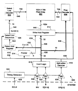
FIG. 6 shows a display driver circuit 600, for driving a display 602 which
includes an
array of pixel cells arranged in 768 rows and 1024 columns. Display driver
circuit 600 includes
select decoder 604, row decoder 606, select line sequencer 608, select address
register 610, write
hold register 612, pointer 614, instruction decoder 616, invert logic 618,
timing generator 620,
and input buffers 622, 624, and 626. Driver circuit 600 receives clock signals
via an SCLK
terminal 628, invert signals via an invert (INV) terminal 630, data and
addresses via a 32-bit
system data bus 632, and operating instructions via a 3-bit op-code bus 634,
all from a system
(e.g., a computer, video signal source, etc.) not shown. Timing generator 620
generates timing
signals, by methods well known to those skilled in the art, and provides these
timing signals to
the various components of driver circuit 600, via clock signal lines (not
shown), to coordinate
the operation of each of the components.
Invert logic 618 receives the invert signals from the system via INV terminal
630 and
buffer 622, and receives the data and addresses from the system via system
data bus 632 and
buffer 624. Responsive to a first invert signal ( INV ), invert logic 618
asserts the received data
and addresses on a 32-bit internal data bus 636. Responsive to a second invert
signal (INV),
invert logic 618 asserts the complement of the received data on internal data
bus 636. Internal
data bus 636 provides the asserted data to write hold register 612, and
provides the asserted
addresses to select address register 610, via 5 (or 24) lines of internal data
bus 636, and to row
decoder 606, via 10 lines of internal data bus 636.
Instruction decoder 616 receives op-code instructions from the system, via op-
code bus
634 and buffer 626, and, responsive to the received instructions, provides
control signals, via an
internal control bus 638, row decoder 606, select line sequencer 608, select
address register 610,
write hold register 612, and pointer 614.
7
CA 02309911 2000-05-12
WO 99/26226 PCT/US98/24216
FIG. 7 shows a table 700, which sets forth op-code instructions for use with
display
driver circuit 600. Each operation is explained with reference to FIG. 6. Op-
code (000)
corresponds to a No Op instruction, to which instruction decoder 616 does not
respond.
Responsive to the system asserting data on system data bus 632 and a Data
Write command
(001) on op-code bus 634, instruction decoder 616 asserts control signals on
control bus 638,
causing write hold register 612 to load the asserted data, via internal data
bus 636, into a first
portion of write hold register 612. Because internal data bus 636 is only 32
bits wide, 32 data
write commands are necessary to load an entire line (1024 bits) of data into
write hold register
612. Pointer 614 provides an address, via a set of address lines 639, to write
hold register 612,
the address indicating the portion of write hold register 612 to which data is
to be written. As
each successive Data Write command is executed, pointer 614 increments the
address to indicate
the next 32-bit portion of write hold register 612.
Responsive to the system asserting a row address on system data bus 632 and a
Load
Row Address command (011) on op-code bus 634, instruction decoder 616 asserts
control
signals on control bus 638 causing row decoder 606 to store the asserted row
address. Then,
responsive to the system asserting a Array Write command (010) on op-code bus
634,
instruction decoder 616 asserts control signals on control bus 638, causing
write hold register
612 to assert the 1024 bits of stored data on a set of data output terminals
640, and causing row
decoder 606 to decode the stored row address and assert a write signal on one
of a set of 768
word-lines 642 corresponding to the decoded row address. The write signal
being asserted on
the corresponding word-line causes the data being asserted on data output
terminals 640 to be
latched into a corresponding row of pixel cells of display 602.
Responsive to the system asserting a block address on system data bus 632 and
a Load
Select Address Register (101) on op-code bus 634, instruction decoder 616
asserts control
signals on control bus 638, causing select address register 610 to store the
asserted block
address, and provide the address, via a set of address lines 644, to select
line sequencer 608.
Then, responsive to the system asserting a Change Pixel States conimand (100)
on op-code bus
634, instruction decoder 616 asserts control signals on control bus 638
causing select line
sequencer 608 to receive the stored block address from select address register
610, convert the
received block address to an initial select line address (e.g., the address of
the first row in the
block), and assert the initial select line address on address lines 646
(SLA[9:0]). Optionally,
select address register 610 includes conversion circuitry for converting the
row address to an
8
CA 02309911 2000-05-12
WO 99/26226 PCT/US98/24216
initial select line address, and provides the select line address to select
line sequencer 608. The
assertion of the initial select line address on address lines 646 causes
select decoder 604 to
decode the initial select line address and assert a pixel update signal on one
of 768 select lines
648 corresponding to the initial select line address. The pixel update signal
on the
corresponding select line causes all of the pixels cells of an associated row
to assert the
previously latched data onto their associated pixel electrodes (not shown in
FIG. 6). Those
skilled in the art will recognize that the conversion of the block address to
the initial select line
address is unnecessary if the system is capable of providing select line
addresses directly.
Responsive to subsequent SCLK cycles, select line sequencer 608 generates a
series of
select line addresses based on the initial select line address, and asserts
the series of select line
addresses on address lines 646. In response to the series of select line
addresses being asserted
on address lines 646, select line decoder 604 decodes each of the select line
addresses and asserts
pixel update signals on corresponding ones of select lines 648.
Those skilled in the art will recognize that any desirable series of select
line addresses
may be generated. For example, the series may continually repeat itself, or
may proceed only
through a predetermined number of addresses and then stop. Additionally, the
series may
increment or decrement by some set value (e.g., 1, 2, or 3), or follow some
other predetermined
sequence. In an alternate embodiment, the system provides a 24-bit block
address to select
address register 610, each bit corresponding to one block of pixel rows in
display 602, the value
of the bit indicating whether or not the corresponding block is to be updated.
Select line
sequencer 608 then generates a series of select line addresses including the
select line addresses
in the blocks which are to be updated, and omitting the select line addresses
in the blocks which
are not to be updated.
In a simple case, the series of select line addresses generated by select line
sequencer 608
is a monotonic, increasing series (e.g., incremented by 1), which begins at
the initial select line
address, cycles through one block (32) of address lines, and then stops. In
this simple case, it
appears to the system that all the pixels in the block are updated
simultaneously in response to a
single Change Pixel States command. To update the next block of pixel cells,
the system
provides another block address on system data bus 632 and a Load Select Line
Register
command on op-code bus 634, to load the new block address into select address
register 610.
Select line sequencer 608, then converts the new block address to another
initial select line
address, and generates another series of select line addresses based on the
new initial select line
9
CA 02309911 2000-05-12
WO 99/26226 PCT/US98/24216
address. Select line decoder decodes the new series of select line addresses,
and updates the
corresponding rows of pixel cells.
FIG. 8 is a timing diagram showing a pixel block being updated while data is
being
loaded. During the first SCLK cycle, the system asserts a Load Select Address
Register
command (101), causing select address register 610 to load the block address
(BA) being
asserted on system data bus 632. During the next SCLK cycle, the system
asserts a Change
Pixel States command (100), causing select line sequencer 608 to assert the
initial select line
address on address lines 646 (SLA[9:0]), thus updating, via decoder 604, the
first row of the
block. During the third clock cycle, the system asserts a Data Write command,
causing 32 bits
of data to be loaded into the first (0th) portion of write hold register 612.
Also during the third
SCLK cycle, select line sequencer 608 asserts the next select line address
(ISA+1) on address
lines 646, causing the next row of pixel cells in the block to be updated.
This sequence
continues until all rows in the block have been updated. It should be
understood that the
commands issued subsequent to the Change Pixel States command (100) are not
necessary to
effect the sequential updating of the rows of the block. The subsequent
commands are shown
only to point out that other commands can be executed concurrently with the
sequential updating
of a block.
From outside of display driver circuit 600, it appears that the entire block
is updated at
once, because only one Change Pixel States command (100) is required to update
the entire
block. In reality, however, because of the internal sequencing of the select
lines, the updating of
each row of pixels is temporally offset from the previous row, thus greatly
reducing the peak
current requirements. Furthermore, because only one Change Pixel States
command (100) is
required to update several discrete groups of pixels (e.g., rows or groups of
rows), the system
interface bandwidth requirement is also reduced.
FIG. 9 shows the effect of the internal sequencing on the block updates. In
particular, the
updating of each block is spread over a longer time interval (compare to FIG.
4). For example,
if a block contains 32 rows, and each row is updated individually, then the
block update is
spread over at least 32 clock cycles.
FIG. 10 shows the temporal offset between the updates of rows within blocks.
Row 0 of
Block 0 updates on the falling edge of the first clock cycle, Row I of Block 0
updates on the
falling edge of the second clock cycle, and so on. While each row update is
shown to be
separated temporally from the previous row update by one clock cycle, those
skilled in the art
CA 02309911 2000-05-12
WO 99126226 PCT/US98/24216
will understand that the row updates may be temporally offset by a greater
number of clock
cycles, without diminishing the effectiveness of the invention.
FIG. 11 shows an alternate display driver circuit 1100, for driving a display
1102 which
includes an array of pixel cells arranged in 768 rows and 1024 columns.
Display 1102 is similar
to display 602, except that each of the 768 rows is divided into 3 sub-rows,
such that each row
update may be temporally spread over at least 3 clock cycles (1 for each sub-
row), further
reducing the peak current requirement as compared to display driver 600 which
updates an entire
row at a time.
Driver circuit 1100 is similar to driver circuit 600, except that select line
decoder 604 is
replaced by select sub-line decoder 1104, which is coupled to 2304 select sub-
lines 1106, each
corresponding to one of the 2304 (768 X 3) sub-lines of display 1102. Further,
select line
sequencer 608 is replaced with select sub-line sequencer 1108, which converts
a received block
address into a 12-bit initial select sub-line address, generates a series of
12-bit select sub-line
addresses based on the initial select sub-line address, and asserts the
generated addresses on
address lines 1110. Select sub-line decoder 1104 decodes each of the select
sub-line addresses
of the generated series and asserts an update signal on a corresponding one of
the select sub-lines
1106.
Those skilled in the art will recognize that select sub-line decoder 1108 can
be designed
to generate any desirable series of select sub-line addresses, providing great
flexibility in
updating display 1102. In a simple case, select sub-line decoder receives a
block address,
converts the block address to the address of the first select sub-line in the
block, and sequentially
updates each sub-row in the block.
FIG. 12 shows one row 1200 of pixel cells (data lines not shown) of display
1102. Row
1200 is divided into 3 sub-rows 1202, 1204, and 1206, which are serviced by 3
separate select
sub-lines 1106(d), 1106(e), and 1106 (f), respectively. Each sub-row 1202,
1204, and 1206 is
updated when select sub-line decoder 1104 (FIG. 11) asserts an update signal
on associated
select sub-lines 1106(d), 1106(e), and 1106 (f), respectively.
FIG. 13 shows another alternate display driver circuit 1300, for driving a
display 1302.
Display 1302 is similar to display 1102 except that each sub-row is serviced
by one select line
and one select sub-line. A particular sub-row is updated when update signals
are simultaneously
asserted on the select line and the select sub-line associated with the
particular sub-row, as will
be explained below with reference to FIG. 14.
11
CA 02309911 2000-05-12
WO 99/26226 PCT/US98/24216
Display driver circuit 1300 is substantially similar to display driver circuit
600, except
for the addition of select sub-line sequencer 1304 and select sub-line decoder
1306. Select sub-
line sequencer 1304 generates a series of select sub-line addresses, and
communicates the
addresses, via a set of address lines 1308, to select sub-line decoder 1306,
which decodes each
address and asserts an update signal on a corresponding one of a set of select
sub-lines 1310(a-
c).
Select line sequencer 608 and select sub-line sequencer 1304 operate together
to
sequentially update the sub-rows of display 1302. Responsive to the system
asserting a Change
Pixel States command (100) on op-code bus 634, instruction decoder 616 asserts
control signals
on control bus 638 causing select line sequencer 608 to generate a series of
select line addresses,
as described above with respect to FIG. 6. The control signals asserted by
instruction decoder
616 also cause select sub-line sequencer 1304 to generate a series of select
sub-line addresses.
The series of select line addresses is synchronized with the series of select
sub-line
addresses to update a block of pixel cells as follows. Select line sequencer
608 asserts an initial
select line address on address lines 646, causing select decoder 604 to assert
an update signal on
a first one of select lines 648 corresponding to an initial row of the block
being updated. At the
same time, select sub-line sequencer 1304 asserts an initial select sub-line
address on address
lines 1308, causing select sub-line decoder 1306 to assert an update signal on
select sub-line
1310(a). The two concurrent update signals cause the first sub-row of the
initial row to be
updated. Next, while the initial select line address is still being asserted
by select line sequencer
608, select sub-line sequencer 1308 sequentially asserts the next two select
sub-line addresses on
address lines 1308, causing select sub-line decoder 1306 to sequentially
assert update signals on
select sub-lines 1310(b) and 1310(c), sequentially updating the second and
third sub-rows of the
initial row. As select line sequencer 608 asserts each successive select line
address of the series,
select sub-line sequencer reasserts the series of select sub-line addresses,
thus updating each row
of the block one sub-row at a time.
The series of select line addresses is synchronized with the series of select
sub-line
addresses at the SCLK level. In particular, a common control signal initiates
the assertion of the
first address by both select line sequencer 608 and select sub-line sequencer
1304. After the
assertion of the initial addresses, select sub-line sequencer 1304 asserts the
next address in the
series of select sub-line addresses every clock cycle, whereas select line
sequencer 608 asserts
the next address in the series of select line addresses every third clock
cycle. ~
12
CA 02309911 2000-05-12
WO 99/26226 PCT/US98/24216
Those skilled in the art will recognize that there are many other ways to
synchronize the
series of select line addresses with the series of select sub-line addresses.
For example, in an
alternate embodiment, select sub-line sequencer 1304 and select line sequencer
608 are replaced
with a single sequencer that generates a 12 bit address, the 2 least
significant bits of the address
being provided to select sub-line decoder 1306 and the 10 most significant
bits being provided to
select line decoder 604. Then, as the 12-bit address is incremented, each
successive row is
updated one sub-row at a time.
FIG. 14 shows the organization of one row 1400(r) of pixel cells of display
1302. Row
1400(r) includes 3 sub-rows of pixel cells 1404(a-c), 3 AND gates 1406, and 3
local select lines
1408. Each AND gate 1406 has a first input terminal coupled to select line
648(r), a second
input terminal coupled to an associated one of select sub-lines 1310(a-c), and
an output terminal
coupled to an associated one of local select lines 1408. Responsive to an
update signal being
asserted on its first and second input terminals by select line 648(r) and an
associated one of
select sub-lines 1310 (a-c), each AND gate 1406 asserts an update signal on
associated local
select line 1408.
Those skilled in the art will understand that rows of pixel cells may be
divided into a
greater or lesser number of sub-rows. In the limiting case, the number of sub-
rows is equal to
the number of pixels in each row, each pixel constituting its own sub-row.
The description of particular embodiments of the present invention is now
complete.
Many of the described features may be substituted, altered or omitted without
departing from the
scope of the invention. For example, those skilled in the art will recognize
that the embodiments
described herein may be modified to drive displays having a greater or fewer
number of rows (or
sub-rows), by providing a sequencer capable of generating an appropriate
address series and a
corresponding number of select lines (or sub-lines). As another example, those
skilled in the art
will recognize that the display driver circuits described herein may be
configured to receive
select line addresses directly from a system, as opposed to receiving a select
line address from a
system by receiving a block address and then generating a select line address
from the block
address, as described herein.
13