Note: Descriptions are shown in the official language in which they were submitted.
CA 02310005 2000-OS-12
002W0 1
SPECIFICATION
FERROELECTRIC MEMORY OR A METHOD OF PRODUCING THE SAME
Technical Field
This invention relates to a non-volatile semiconductor
device having a ferroelectric layer, more specifically to
improvement in partial voltage applied to the ferroelectric
layer.
Background Art
FIG. 9 shows a cross section of an essential part of a
conventionalferroelectric memory50. The ferroelectric memory
50 comprises a semiconductor substrate 51 on which are formed
in succession; a gate oxide film 54, a floating gate electrode
55, a ferroelectric layer 56, and a control gate electrode 57.
In the ferroelectric memory 50, not much part of the voltage
applied to the control gate 57 for switching polarized state
is applied to the ferroelectric layer 56. This is because the
dielectric constant F of the ferroelectric is much greater
(several hundred times) than that of Si02 or the like, and the
capacitance of the ferroelectric layer 56 is much greater than
that of the gate oxide film 54. The partial voltages on
capacitors connected in series are inversely proportional to
their capacities.
To solve the problem, it is proposed for example in the
Transaction of 14th Ferroelectric Application Convention,
CA 02310005 2000-OS-12
002W0 2
"Development of Low Dielectric Constant Ferroelectric Material
for MFMISFET" (14th Ferroelectric Application Convention,
issued September 1997, pages 31 - 32) to reduce the capacitance
of the ferroelectric layer bydevelopinga ferroelectricmaterial
of a smaller dielectric constant, or to increase the capacitance
of the insulation film by reducing the thickness of the gate
oxide film. However, there is limitation of development of
materials. Reducing thickness of the gate oxide film results
in a lower dielectric resistance.
A ferroelectric memory transistor 101 shown in FIG. 10 which
is intended to solve the above problems is disclosed in
JP-A-9-252099. Fig. lOB shows a section XB-XB in FIG. 10A.
Theferroelectric memory transistorlOlcomprises, asshown
in FIGs. l0A and lOB, a floating gate electrode 124 in the active
region 168, on which is formed an insulation film 130, and on
which is a ferroelectric layer 134 . A contact hole 132 is formed
in the inactive region 130. The floating gate electrode 124
and the ferroelectric layer 134 are in mutual contact in the
inactive region 130.
In the ferroelectric memory transistor 101, the partial
voltage between the floating gate electrode 124 and the substrate
region 112 can be reduced and the partial voltage between the
floating gate electrode 124 and a control gate 136 can be increased
by only changing the area of the contact hole 132 . The capacitor
constituted between the control gate 136 and a P well 112 in
the ferroelectric memory transistor 101 has a capacitance
equivalent to the resultant capacitance shown in FIG. lOC in
CA 02310005 2000-OS-12
002W0 3
which capacitors CF and CG are connected in series. The
capacitance CF is a resultant capacitance resulting from the
parallel connection of the capacitors C1 and C2 . The capacitance
C1 is a capacitance defined with the insulation film 130 and
the ferroelectric layer 134 on the active region 168, while the
capacitance C2 is a capacitance defined with the ferroelectric
layer 134 on the element separation region 114. Since the
ferroelectric layer is much higher in dielectric constant than
the insulation film, the capacitance CF may be approximated with
the capacitance C2 . Therefore, the capacitance CFmay be reduced
by reducing the capacitance C2 . This makes it possible to reduce
the partial voltage applied to the capacitor CG and increase
the partial voltage applied to the capacitor CF.
However, even if the partial voltage between the floating
gate electrode 124 and the substrate region 112 is reduced and
the partial voltage between the floating gate electrode 124 and
the control gate electrode 136 is increased, then the partial
voltage applied to the ferroelectric layer 134 on the active
region 168 cannot be increased much. This is because the
insulation film 130 is much smaller in dielectric constant than
the ferroelectric layer 134 and higher partial voltage is applied
to the insulation film 130 than to the ferroelectric layer 134
on the active region 168.
Also it is disclosed in JP-A-9-205181, to reduce opposing
area by reducing the upper electrode . However, since this method
uses the ion milling process, the surface of the ferroelectric
layer is damaged.
CA 02310005 2000-OS-12
Q02W0 4
The above-described problem of reduced partial voltage
associated with the ferroelectric memory constituted with the
gate insulation film, floating gate electrode, ferroelectric
layer, and control gate electrode also occurs in the
ferroelectric memory in which there is no floating gate electrode
between the gate insulation film and the ferroelectric layer.
Disclosure of the Invention
The object of the invention is to provide a ferroelectric
semiconductor memory device capable of solving the
above-described problems, namely capable of applying higher
partial voltage by reducing the substantial area of the
ferroelectric layer.
The ferroelectric semiconductor memory device of the
invention comprises:
A)
al) a semiconductor substrate having a substrate region
of a first conductive type:
a2 ) a pair of impurity regions of a second conductive type
formed on the surface of the first conductive region;
a3) a first insulation film formed on the substrate region
between the pair of impurity regions;
a4) a ferroelectric layer formed on the first insulation
film;
a5 ) an upper electrode formed on the ferroelectric layer;
and
B)asubstantialcapacitance reducinginsulation film formed
CA 02310005 2000-OS-12
002W0 5
between the first insulation film and the upper electrode and
only on part of the substrate region between the pair of impurity
regions to reduce substantial capacitance of the ferroelectric
layer.
The ferroelectric semiconductor memory device of the
invention is characterized by comprising:
A)
al) a semiconductor substrate having a substrate region
of a first conductive type;
a2 ) a pair of impurity regions of a second conductive type
formed on the surface of the first conductive region;
a3) a first insulation film formed on the substrate region
between the pair of impurity regions;
a4) a ferroelectric layer formed on the first insulation
film;
a5) an upper electrode formed on the ferroelectric layer;
and
B) a substantial capacitance reducing insulation film formed
between the first insulation film and the upper electrode to
reduce substantial capacitance of the ferroelectric layer, and
having, on the substrate region between the pair of impurity
regions, a portion in which only the ferroelectric layer is
present and a portion in which the capacitance reducing
insulation film and the ferroelectric layer are present in
superimposed state.
The method of manufacturing the ferroelectric memory device
of the invention is characterized by comprising the steps of:
CA 02310005 2000-OS-12
002W0 6
A)
al) providing a semiconductor substrate having a substrate
region of a first conductive type;
a2) forming a first insulation film in part of the substrate
region and on the substrate region;
a3) forming a ferroelectric layer and an upper electrode
on the first insulation film;
a4 ) forming an impurity region of a second conductive type
in the substrate region by implanting the second conductive type
of impurity using the upper electrode as a mask; and
B) forming a capacitance reducing insulation film between
the first insulation film and the upper electrode to reduce
substantial capacitance of theferroelectric layer, and having,
on the substrate region and in the lower region of the upper
electrode, a portion in which only the ferroelectric layer is
present and a portion in which the capacitance reducing
insulation film and the ferroelectric layer are superimposed.
The semiconductor memory using a ferroelectric layer of
the invention is the one having a ferroelectric memory FET in
which a control gate electrode is provided on a semiconductor
layer through at least a first insulation film and a ferroelectric
layer, with a second insulation film being inserted in part of
the upper or lower side of the ferroelectric layer corresponding
to part of the area of the ferroelectric layer.
Those features and other objects, applications, effects,
etc. of this invention will be apparent in reference to the
embodiments and appended drawings.
CA 02310005 2000-OS-12
002W0 7
Brief Description of the Drav~ings
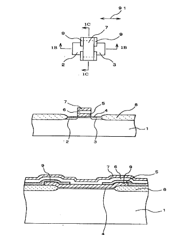
FIG. 1 is an explanatory drawing of the structure of a
ferroelectric FET portion of a semiconductor memory as an
embodiment of the invention;
FIG. 2 is an explanatory drawing of an equivalent circuit
of the capacitor portion in FIG. 1;
FIG. 3 is a plan view showing a manufacturing process;
FIGS. 4A, 4B and 4C are cross-sectional views of essential
parts in FIGS. 3B, 5A and 5B;
FIGs. 5A and 5B are plan views showing a manufacturing
process;
FIGS . 6A and 6B are cross-sectional views of essential parts
in FIG. 5B;
FIG. 7 is a structural drawing of a memory constituted by
arranging the FET portion of FIG. 1 in a matrix pattern;
FIGS. 8A, 8B, 8C and 8D show cross sections in FIG. 7;
FIG. 9 shows a cross section of an essential part of a
conventional ferroelectric FET; and
FIGS . 10A, lOB and lOC show conventional ferroelectric FETs .
Best Mode for Carrying out the Invention
The inventors have found a method of substantially reducing
the capacitor area constituted with a ferroelectric layer without
etching the ferroelectric layer if a second insulation film of
a small dielectric constant is interposed on the top or under
side of the ferroelectric layer to be etched. If it is possible
CA 02310005 2000-OS-12
002W0 8
to make the capacitor area constituted with the ferroelectric
layer being smaller than the capacitor area constituted with
a gate oxide film, then the partial voltage applied to the
ferroelectric layer may be increased. In order to reduce the
capacitor area constituted with the ferroelectric layer, it is
conceivable to etch the ferroelectric layer on the floating gate
electrode. However, when the ferroelectric layer is etched on
the floating gate electrode, the floating gate electrode is
exposed and comes into contact with the control gate electrode .
Thisrequiresanotherinsulation filmto be provided. Moreover,
the ferroelectric layer is very difficult to etch.
A ferroelectric memory 1 as a ferroelectric semiconductor
device according to the invention will be hereinafter described
in reference to the appended drawings.
FIG. 1A is a plan view of the ferroelectric memory 1. FIGS.
1B and 1C show cross sections, along the lines 1B-1B and 1C-1C
in FIG.lA, respectively.
In the ferroelectric memory 1 shown in FIG. 1B, an n-type
drain region 2 and a source region 3 are formed in a p-type
semiconductor layer or well la. A gate oxide film 4 as a first
insulation film is formed on the semiconductor layer 1 between
the drain region 2 and the source region 3. A gate electrode
5 of a floating type, a ferroelectric layer 6, and a control
gate electrode 7 as an upper electrode are successively formed
on the gate oxide film 4. As shown in FIG. 1C, a silicon oxide
film 9, as a capacitance reducing insulation film of a dielectric
constant smaller than that of the ferroelectric layer, is
CA 02310005 2000-OS-12
002W0 g
provided between the floating gate 5 and the ferroelectric layer
6, excluding the approximately central portion of the active
region.
The silicon oxide film 9 is provided as shown in FIGs. lA
and 1C on the floating gate electrode 5 so as to cover both end
areas, in the direction at right angles to the direction in which
the drain region 2 and the source region 3 are provided, of the
floating gate electrode 5. The silicon oxide film 9 is formed
in a thickness of about, 100 to 3000 angstroms by the CVD process
or the like.
The silicon oxide film 9 as described above reduces the
substantial area of the capacitor constituted with the
ferroelectric layer 6. The thickness of the silicon oxide film
9 is preferably about, 100 to 3000 angstroms. When the thickness
is too small, as will, be described later, the effect of reducing
the capacitance becomes weak due to the ratio of dielectric
constants. When the thickness is too great, the film forming
and pattern making take much time. The thickness of the silicon
oxide film 9 is more preferably about 100 to 500 angstroms . The
silicon oxide film 9 is preferably formed on the floating gate
electrode 5 excluding the portion serving as an active region
( channel region) surrounded with the drain region 2 and the source
region 3.
Now, the function of the capacitance reducing insulation
film (second insulation film) will be described. The
capacitance reducing insulation film has a dielectric constant
sufficiently smaller than that of the ferroelectric layer.
CA 02310005 2000-OS-12
OD2W0 10
Therefore, when considering the resultant capacitance, the
portion of the capacitance reducing insulation film may be
substantially neglected. Asa result, the dielectric capacitor
area substantially decreases.
As shown in FIG. 2, the capacitance C2 between the control
gate electrode and the floating gate electrode in the
ferroelectricmemory FET is expressed with the following equation
(1)
C2 = Cl + a CF --------------- (1)
where a : ratio of the area not provided with the capacitance
reducing insulation film to the ferroelectric layer area
surrounded with both electrodes, CF: the capacitance of the
ferroelectriclayer,Cl:the resultant capacitance produced with
the capacitance of the capacitance reducing insulation film in
the part where the capacitance reducing insulation film is
provided and with the capacitance of the ferroelectric layer.
The resultant capacitance Cl is expressed with the following
equation:
1/Cl = 1/Ci + 1/(1 - a)CF --------------- (2)
where Ci: the capacitance of the capacitance reducing
insulation film.
As already explained, the capacitance reducing insulation
film has a dielectric constant sufficiently smaller than that
of the ferroelectric layer (CF ) Ci). Therefore, from the
equation (2),
C1 T Ci -______-_______ (3)
Hence, from the equations (1) and (3),
CA 02310005 2000-OS-12
002W0 11
C2 = Ci + a CF --------------- (4)
Here, since CF O Ci,
C2 = a CF --------------- (5)
Therefore, the capacitance in the ferroelectric memory FET
is as shown in FIG. 2 nearly equivalent to the resultant
capacitance produced with the series connection of a CF and the
capacitance CoX of the gate insulation film. Therefore, the
partial voltage VF applied to the ferroelectric layer is
approximated as,
VF = CoX~VOX/aCF (a < 1)
Therefore, the partial voltage VF is increased by the decrease
in the value of a.
That is to say, if CF O Ci, the portion where the capacitance
reducing insulation film is present may be neglected, and it
may be regarded as a stacked capacitor in which the area of the
ferroelectric layer is reduced (by a times) . As a result, as
shown in FIG. 1C, the area of the ferroelectric capacitor is
smaller than the capacitor area of the gate oxide film (Si02) .
The material of the capacitance reducing insulation film
may be any material as long as it can make the capacitance Ci
sufficiently smaller than the capacitance CF as described above.
For example, using PZT ( Pb ( Zr, Ti ) 03) as the ferroelectric, having
a dielectric constant of F - 800 and a film thickness of 2000
angstrom and Si02 as the capacitance reducing insulation film,
having a dielectric constant of f - 3.9 and a film thickness
of 3000 angstrom, and if a = 1/3:
CF = 800 ~ f 0 ~ S/2 x 10 ', Ci = 3 . 9 ~ ~ 0 ~ S/3 x 10-', and CF/Ci
CA 02310005 2000-OS-12
a
002W0 12
- 923.08, and thus it may be assumed that CF » Ci,
Here, f0 denotes the dielectric constant of vacuum, and
S denotes area.
As a result, even if the same voltage is applied to the
control gate electrode, a voltage three times (1/ a ) higher than
in conventional arrangement can be applied to the ferroelectric
layer according to the equation (5).
Incidentally, the silicon oxide film 9 may be provided either
on top or under side of the ferroelectric layer as long as it
is provided between the floating gate electrode 5 and the control
gate electrode 7.
Likewise in the MFIS structure having no floating gate
electrode, the capacitance reducing insulation film may be
provided either on top or under side of the ferroelectric layer
as long as it is provided under the control gate electrode 7.
In this embodiment, while the silicon oxide film 9 is formed
in other than approximate central part of the active region,
there is no limitation for the location; an arrangement suffices
that a region where no capacitance reducing film exists, namely
a region where the capacitance reducing film does not overlap
with the ferroelectric layer, is present between the floating
gate electrode and the control gate electrode in the active
region.
Incidentally, while the width of the silicon oxide film
9 in the direction of arrow 91 in FIG. lA is formed to be greater
than that of the upper electrode, it may be formed with the same
width. This allows to etch in the width direction collectively
CA 02310005 2000-OS-12
002W0 13
at a time using a photo resist after laminating a conductive
layer for the upper electrode. The manufacturing process in
this case will be described in reference to FIGS. 3 to 5.
Incidentally, the hatched areas in FIGs. 3A, 3B, 5A and
5B do not mean cross sections but visual discrimination from
other parts. This also applies to FIG. 6 which will be described
later.
As shown in FIG. 3A, LOCOS oxide films 8 are formed in a
p-type well la of the semiconductor substrate 1. Then the p-type
well la is divided into elements in lateral and vertical row
directions by the LOCOS oxide films 8 thus formed. A 100 angstrom
thick gate oxide film 4 is formed. Platinum is deposited over
the entire surface and, using a mask of photo resist, an electrode
layer 25 for the floating gate is formed as shown in FIG. 3B.
The material for the electrode layer 25 may be selected in
consideration of lattice compatibility with the ferroelectric
layer formed on the layer 25 and of the crystallization process
when the ferroelectric layer 6 is formed. FIG. 4A shows a cross
section taken along the line IVA-IVA in FIG. 3B
A 200 angstrom thick silicon oxide film is deposited over
the entire surface using the CVD process, and as shown in FIG.
5A, a silicon oxide film (insulation layer) 9 is formed to cover
the electrode layer 25 for the floating gate electrode on the
active region except the approximate central part of the
electrode layer 25 using a mask of photo resist. FIG. 4B shows
a cross section taken along the line IV B-IV B in FIG. 5A.
Incidentally, in place of the silicon oxide film 9, an insulation
CA 02310005 2000-OS-12
402W0 14
film of a small dielectric constant such as silicon nitride film
and Ti02 may be used.
Next, a ferroelectric layer is formed over the entire surface .
The film is formed with a material of perovskite structure such
as titanium oxide zirconium oxide lead (PZT), titanium oxide
zirconium oxide lanthanum lead (PLZT), tantalum oxide bismuth
strontium (SBT-based) by sputtering or sol-gel method, and then
is subject to heat treatment. Over that entire surface is
deposited a platinum layer for forming a control gate electrode
by the sputtering.
Using a mask of photo resist, as shown FIG. 5B, the width
direction(arrow 90) parts of the floating gate electrode 5,
silicon oxide film 9, ferroelectric layer 6, and the control
gate electrode 7 are formed. FIG. 4C shows a cross section taken
along the line IVC-IVC in FIG. 5B.
Section IVA-IVA in FIG. 5B is shown in FIG. 6A. Section IV
B-IVB in FIG. 5B is shown in FIG. 6B. In this way, in the
approximate central part of the active region, two layers of
the ferroelectric layer 6 and the control gate electrode 7, are
stacked on the floating gate electrode 5. In the end portion
of the active region, three layers of the silicon oxide film
9, ferroelectric layer 6 and the control gate electrode 7, are
stacked on the floating gate electrode 5.
Thereafter, the process may follow the steps for ordinary
ferroelectric memory: N-type impurity is ion-implanted using
the control gate electrode as a mask to form the drain region
2 and the source region 3 by self-alignment method. Interlayer
CA 02310005 2000-OS-12
002W0 15
insulation film is formed over the entire surface by the CVD
process, and drain lines and source lines are formed.
While this embodiment is described for the case in which
the capacitance reducing insulation film 9 is formed between
the floating gate electrode 5 and the ferroelectric layer 6,
it may be formed between the ferroelectric layer 6 and the control
gate electrode 7 . That is, it may be formed between the floating
gate electrode 5 and the control gate electrode 7.
Also the capacitance reducing insulation film may be formed
similarly in the MFIS structure having no floating gate electrode.
In that case, the process of forming the floating gate shown
in FIG. 3B may be omitted.
Next, an example of constituting a memory by arranging the
ferroelectric memories of the above-described structure in a
matrix pattern will be described in reference to FIGS. 7 and
8.
FIG. 7 is a plan view of one example of such configuration.
FIGS. 8A, 8B, 8C, and 8D respectively show explanatory cross
sections VIQA-V1QA, V1QB-V1QB, V1QC-VIQC, and V1QD-VIQD in FIG. 7.
FIG. 7 shows four ferroelectric memory FETs (memory cells
Ql through Q4) formed. Incidentally, in FIGS. 7 and 8, the gate
oxide film and the floating gate electrode are left out of
illustration.
As shown in FIG. 8A, a p-type well la is provided on a substrate
1. As shown in FIGS. 7, 8A and 8D, the well la is divided in
the vertical row direction with LOCOS oxide films 8, and in the
lateral direction with deep isolation trenches 15.
CA 02310005 2000-OS-12
002W0 16
As shown in FIG. 8A, an n-type drain region 2 and a source
region 3 are formed in the well la . On part of the well 1a between
the drain region 2 and the source region 3, a gate oxide film
(not shown) and a floating gate electrode (not shown) are formed.
The control gate electrode 7 is formed on the floating gate
electrode through the ferroelectric layer 6.
As shown in FIG. 7, the control gate electrode 7 constitutes
word lines WL1, WL2 formed in succession in the lateral row
direction. As shown in FIG. 8C, an insulation film 9 as a second
insulation film is provided between the ferroelectric layer 6
and the control gate electrode 7.
An interlayer insulation film 12 is formed on the control
gate electrode 7. As shown in FIGs. 8A and 8B, source lines
SL1 and SL2 connecting source regions 3 of respective cells
arranged in lateral rows as seen in FIG. 7 are formed on the
interlayer insulation film 12.
An interlayer insulation film 13 is formed on the source
lines SLl and SL2. As shown in FIGs. 8A through 8D, data lines
DL1 and DL2 connecting drain regions 2 arranged in the vertical
rows as seen in FIG. 7 through first metal layers 11 are provided
on the interlayer insulation film 12.
Thus, a semiconductor memory can be constituted in which
memory cells are provided in a matrix pattern.
The well la divided in the lateral row direction with the
deep isolation trenches 15 serves as bit lines BL1 and BL2 (not
shown) extending parallel to the drain lines. The well la may
be provided with contacts spaced at equal intervals so as to
CA 02310005 2000-OS-12
002W0 17
lower its resistance.
The ferroelectric memory device of this invention is
provided with the substantial capacitance reducing insulation
film for reducing substantial capacitance of the ferroelectric
layer, formed on only part of the substrate region between the
pair of impurity regions and between the first insulation film
and the upper electrode. Therefore, the partial voltage for
the ferroelectric layer can be increased. This enables the
memory device to be driven with a low writing voltage.
In the ferroelectric memory device of this invention, the
substantial capacitance reducing insulation film is smaller in
dielectric constant than the ferroelectric layer. Therefore,
the partial voltage for the ferroelectric layer can be increased
even with a smaller area of the firm.
In the ferroelectric memory device of this invention, the
substantial capacitance reducing insulation film for reducing
substantial capacitance of the ferroelectric layer is formed
between the first insulation film and the upper electrode, and
on the substrate region between the pair of impurity regions,
and there are a portion where only the ferroelectric layer is
present and a portion where the capacitance reducing insulation
film and the ferroelectric layer are present in overlapped state.
Therefore, the partial voltage for the ferroelectric layer can
be increased. This enables the memory device to be driven with
a low writing voltage.
Inthesemiconductor memory having theferroelectric memory
FET of this invention, a second insulation film is located at
CA 02310005 2000-OS-12
002W0 18
the upper or under side of the ferroelectric layer corresponding
to part of the area of the ferroelectric layer. Therefore, the
substantialcapacitance of theferroelectriclayer can be reduced.
This enables the memory device to be driven with a low writing
voltage.
The manufacturing method of theferroelectric memory device
of this invention is characterized by comprising the step of
forming a capacitance reducing insulation film between the first
insulation film and the upper electrode to reduce substantial
capacitance of the ferroelectric layer, on the substrate region
and in the lower region of the upper electrode, to provide a
portion in which only the ferroelectric layer is present and
a portion in which the capacitance reducing insulation film and
the ferroelectric layer are superimposed.
Therefore, it is possible to provide a ferroelectric memory
device with which the partial voltage on the ferroelectric layer
is increased.
The semiconductor memory using the ferroelectric layer of
this invention is one having a ferroelectric memory FET in which
a control gate electrode is provided on a semiconductor layer
through at least a first insulation layer and a ferroelectric
layer, with a second insulation film being inserted in a position
that is on top or under side of the ferroelectric layer and
corresponds to part of the area of the ferroelectric layer.
With the above-described constitution, the capacitance of
part of the ferroelectric layer having the second insulation
film is reduced, and the part may be seen as an insulation member
CA 02310005 2000-OS-12
002W0 19
in an electric circuit, and the same effect is provided as in
the case in which the capacitance with the ferroelectric layer
is reduced to that with the area where the second insulation
film is not present. As the capacitance with the ferroelectric
layer is reduced, partial voltage applied to the ferroelectric
layer increases.
It is preferable that the second insulation film is made
of a material having a smaller dielectric constant than that
of the ferroelectric layer, because the effect of reduced
substantial area of the ferroelectric layer increases due to
reduced capacitance of that part.
Specifically, it is possible for example to constitute the
ferroelectric memory FET in which; a floating gate electrode
is disposed between the semiconductor layer and the control gate
electrode, the ferroelectric layer is disposed between the
floating gate electrode and the control gate electrode, and the
second insulation layer is disposed between the floating gate
electrode and the control gate electrode.
The ferroelectric memory of this invention has an insulation
film to reduce the effective area of the ferroelectric layer.
Therefore, a high partial voltage can be applied to the
ferroelectric layer. As a result, the ferroelectric memory FET
can be driven with a low drive voltage. That is, it is eliminated
to; use a special ferroelectric material, make the gate oxide
film too thin, or apply a special process to the ferroelectric
layer.
While the invention is described above by way of preferred
CA 02310005 2000-OS-12
002W0 20
embodiments, the terms used herein are not for limitation but
for explanation only, and may be changed or modified within the
scope of the appended claims without departing from the scope
and spirit of the invention.