Note: Descriptions are shown in the official language in which they were submitted.
CA 02310057 2000-OS-16
wo ~r~sst~8 pcrms9siz3z9~
A METHOD FOR MINIMIZING THE CRITICAL DIMENSION
GROWTH OF A FEATURE ON A SEMICONDUCTOR WAFER
Field of the Inv~ try ion:
The present invention is directed to a method for minimizing the
critical dimension growth of a feature on a semiconductor wafer.
Background of the inven~,on:
The critical dimension (CD) of a feature on a semiconductor
wafer is the width of that feature. The pitch is generally defined as
the critical dimension plus the distance to the next feature.
For semiconductor processing methodology using etch
techniques, a photoresist layer is deposited on top of a material to be
etched. The photoresist layer defines the desired features, masking
the portion of the layer which is not to be etched and leaving exposed
the portion to be etched. During the etching process, materials from
a portion of the layer which is etched as well as compounds formed by
a combination of the etchant gases and the materials of the layer to be
etched, can tend to coat the sides of the desired feature and thereby
2o increase the critical dimension of the feature beyond that defined
immediately under the photoresist mask. Such growth of the critical
dimension can disadvantageously diminish the distance between the
features and adversely affect the functionality of the features.
Accordingly, there is a need to provide a semiconductor
processing methodology which allows for the desired features to be
appropriately etched without causing a growth of the critical dimension
of the feature during the etching process.
CA 02310057 2000-OS-16
WO 99!25568 PCT/US98l23297
-Z-
Summanr of the Invention:
The present invention provides for a methodology which allows
for etching of features while minimizing the growth of the critical
dimension of the feature during the etched process. The method of
the invention determines a direct correlation between the temperature
of the wafer during the etch process and the growth of the critical
dimension of a feature. In particular, it has been found that the
growth of the critical dimension of a feature can be minimized by
elevating the temperature of the wafer during the semiconductor
processing.
Accordingly, it is an object of the present invention to control
and minimize the growth of the critical dimension of a feature on a
semiconductor wafer.
It is a further object of the present invention to minimize the
growth of the critical dimension by increasing the temperature of the
wafer to a level which discourages the growth of the critical
dimension.
It is a further object of the present invention to control the
critical dimension of the feature during an etch process by controlling
the temperature of the wafer.
It is another object of the present invention to minimize the
growth of the critical dimension by reducing heat transfer from a chuck
holding the wafer in order to increase the temperature of the wafer.
It is still a further object of the present invention to control the
critical dimension of the feature by heating a chuck in order to raise
the temperature of the wafer.
It is still a further object of the present invention to perform the
methodology of minimizing the critical dimension of a feature during a
low pressure semiconductor etch process conducted in the millitorr
CA 02310057 2000-OS-16
WO 99125568 PG"f/US98/Z3Z97
-3-
range with the backside of a wafer kept in contact with a source of
gas in the about zero to about 10 torr range in order to reduce the
cooling of the wafer due to reduced heat transfer through the gas.
Accordingly, the invention included the method for minimizing
the critical dimension growth of a feature located on a wafer during an
etch process including the steps of placing a wafer on a chuck in an
etch reactor and etching the wafer in the etch reactor. The method
further includes allowing the temperature of the wafer to climb to the
range of about 130°C to about 300°C in order to minimize the
critical
dimension growth of the feature located on the wafer.
In another aspect of the invention, the method for minimizing
critical dimension growth of a feature located on the wafer during an
etch process includes the steps of placing a wafer on a chuck in a etch
reactor and controlling the temperature of a wafer by maintaining a gas
in contact with a backside of the wafer.
The process further includes etching a wafer in the etch reactor
and allowing the temperature of a wafer rise in order to minimize the
critical dimension growth of a feature located on the wafer by reducing
the pressure of the gas in contact with the backside of the wafer.
2o A further aspect of the invention includes minimizing the critical
dimension growth of a feature located on a wafer during an etch
process including the steps of placing a wafer on a chuck in an etch
reactor and controlling the heat transfer from the wafer in order to
allow the temperature of the wafer to climb in order to minimize the
critical dimension growth of the feature on the wafer.
Other objects, advantages, and features of the invention will be
described hereinbelow and evidenced in the claims and figures.
CA 02310057 2000-OS-16
_ WO 99/ZSS68 PCT/US98123297
-4-
Brief Descriution of the Figures
Fig. 1 depicts a wafer temperature versus clamp pressure chart
showing the wafer temperature rising over time at increasing lower
clamp Iwafer backside) pressures.
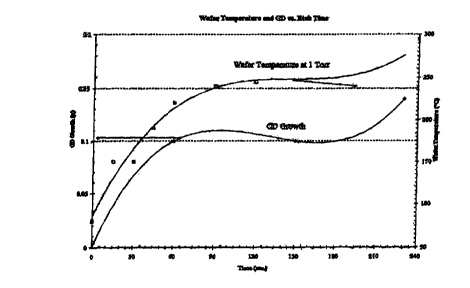
Fig. 2 depicts a chart of critical dimension growth and wafer
temperature versus etch time wherein the growth of the critical
dimension is reduced and plateaus at elevated wafer temperatures and
reduced clamp (wafer backside) pressures.
Figs. 3a and 3b are SEM pictures, perspective and side
1o elevational views of a starting photoresist pattern where the critical
dimension is 0.19 microns.
Figs. 4a and 4b depict the perspective and side elevational
views similar to those of Figs. 3a and 3b at 60 seconds into etch when
the critical dimension is 0.29 microns.
Figs. 5a and 5b depict the perspective and side efevational
views similar to those of Figs. 3a and 3b at end point of about 150
seconds where the critical dimension remains at 0.29 microns.
Figs. 6a and 6b depict the perspective and side elevational
views similar to those of Figs. 3a and 3b at about 230 seconds which
2o is approximately 50% over-etch where the critical dimension has
grown to 0.34 microns.
Fig. 7 depicts an etch reactor wherein the method of the present
invention can be carried out.
Fig. 8 depicts a cross-sectional view of chuck used with the
etch reactor of Fig. 7.
Detailed Description of the Preferred Embodiment
The method of the present invention can be performed in an
etch reactor such as the etch reactor depicted in Fig. 7 using the
3o chuck configuration such as the chuck configuration shown in Fig. 8.
CA 02310057 2000-OS-16
WO 99125568 PCT/US98123297
-5-
It is to be understood that other reactors including but not limited to
other etch reactors and other chuck configurations can be used and be
within the scope and spirit of the invention.
The etch reactor of Fig. 7 is identified by the number 20 and is
configurated as a tri-electrode reactor. The etching apparatus 20
includes a housing 22 and an etching chamber 24. A wafer 26 is
positioned on a bottom electrode 28. The chamber 24 further includes
side peripheral electrode 30 and an upper electrode 32. In a preferred
embodiment, the side peripheral electrode 30 can be grounded or
allowed to establish a floating potential as a result of the plasma
developed in the chamber 24. The upper electrode 32 is generally
grounded. In typical operation, both the side peripheral electrode 30
and the upper electrode 32 are grounded as shown in Fig. 7.
Preferably two A.C. power supplies, first power supply 34 and
second power supply 36, are connected to the bottom electrode 28
through a appropriate circuitry 38 which includes matching networks
and a combiner. Further a controller 40 controls the sequencing of the
first and second AC power supplies 34, 36. Typically, the first power
supply 34 operated in the kilohertz range and is optimally provided at
about 450 KHz, and typically in the range of less than 500 KHz. The
second power supply 36 operates in the megahertz range, and
typically operates at about 13.56 MHz, although other frequencies
above about 1 MHz and also multiples of 13.56 MHZ can be used with
the present invention. The power supply 34 is powered at 200 watts
and the second power supply 36 is powered at 500 watts for this
example. ion energy increases towards the kilohertz range while ion
density increases towards the megahertz range. Additionally, reactor
20 includes gas inlet head 42 and a gas outlet port 44.
CA 02310057 2000-OS-16
WO 99/25568 !'CT/US98123297
.g_
Turning to Fig. 8, the chuck which is incorporated in the bottom
electrode 28 is shown in greater detail. As can be seen in Fig. 8, the
chuck configuration 46 includes a wafer clamp 48 which is spring
loaded using springs 50 in order to hold a wafer 26 against the lower
electrode 28. The gas which controls heat transfer from the wafer is
delivered in the gas delivery space 54 located between the wafer 26
and the lower electrode 28. In a preferred embodiment, the wafer
claim 48 is made of a high purity alumina ceramic and the
configuration is set up that when the gas contained in gas delivery
1o space 54 is helium that the gas leak rate into the reactor chamber 24
is on the order of less than 2 SCCM with a typical process flow rate
being for example, 80 SCCM.
As will be explained below, alternative to or in addition to the
modification of heat transfer from the wafer due to the control of the
gas pressure (wafer clamp pressure) in the gas delivery space 54, the
chuck 46 can itself be heated in order to heat the wafer. Such heating
can be the result of, for example, a resistive heater 56 contained in the
lower electrode 28. Other wafer heating apparatus can be used.
Turning to Fig. 1, a chart is shown which depicts the rise in
2o temperature of the wafer over time based on the pressure of the gas
located in the gas delivery space 54. For this particular chart in Fig.
1 and also in Fig. 2 and also for purposes of the SEM pictures of Figs.
3a, 3b, to 6a, 6b, the reactor 20 in Fig. 7 is operated in a low pressure
region of about 1 millitorr to about 100 millitorr and in this particular
example at approximately 5 millitorr for performing a platinum etch
with a chlorine flow rate of 9 SCCM and argon flow rate of 20 SCCM
for about 230 seconds. The gas delivered to the gas delivery space
54 is helium, as helium has a good heat capacity, is light and mobile,
and is efficient in transferring energy. Other gases such as nitrogen
3o and argon could be used, and in addition any gas that has these
CA 02310057 2000-OS-16
WO 99125568 PGTIUS9$/23297
_7_
characteristics and which will not condense could be used. It will be
understood that at least some of these gas will leak into the main
reaction chamber 24.
In Fig. 1, four curves are plotted. The curves are for helium
pressures of approximately 0 torn, 1 torr, 3 torr, and 5 torr, in the gas
delivery space 54. As can be seen generally in Fig. 1, at about 3 torr
and greater, the wafer surface temperature goes from about 80°C to
about 140° C within the first 60 seconds. At a helium pressure of
about 1 torr in the gas delivery space 54, the wafer surface
o temperature goes from about a starting temperature of about 80°C to
over 200°C in the first 60 seconds and finally levels off at around
240°C. Also as shown in Fig. 1 at close to 0 torr, the temperature of
the wafer hits approximately 300°C in the first 60 seconds and it
continues to climb due to the lack of heat transfer from the wafer at
such a low pressure for the gas in the gas delivery space 54.
Turning to Fig. 2, a time frame of 0 to 240 seconds for a etch
process is displayed. This etch process is with the helium in the gas
delivery space 54 held at 1 torn and using al! the other characteristics
and parameters for gas flow, power and low pressure, as identified
with respect to Fig. 1. In this method, the electrode 28 starts at about
80°C. As can be seen in Fig. 2, with these parameters, in the first 60
seconds the wafer temperature rises from about 80°C to about
230°C.
Simultaneous with this rise in temperature, the critical dimension of the
feature grows approximately 0.10 microns during the first 60 seconds
of the etch processing. Further, as can be seen in Fig. 2, for the time
frame of about 60 seconds to about 150 seconds, or for the bulk of
the etch process time (90 seconds), there is substantially no growth
in the critical dimension as the growth plateaus. After about 150
seconds, the growth continues adding approximately 0.05 microns
3o during the over-etch step from between about 150 seconds to about
CA 02310057 2000-OS-16
WO 99125568 PCT/US98n3297
_g_
230 seconds. This over-etch process time is approximately 80
seconds. During the over-etch time of between 150 seconds to 230
seconds, the temperature of the wafer climbs from about 250°C to
about 275°C. For the example shown in Fig. 2, Figs. 3a, 3b, 4a, 4b,
5a, 5b, 6a, and 6b, show the profile of the feature and demonstrate
the growth of the critical dimension of the feature during the process.
In Figs. 3a, 3b, the starting pattern of the photoresist and the critical
dimension of 0.19 microns is depicted. In Figs. 4a, 4b, after 60
seconds of etch, the critical dimension is approximately 0.29 microns
(also see Fig. 2). At etch end point, as shown at Figs. 5a, 5b, the
critical dimension still remains at the plateau of 0.29 microns. At 50%
of over-etch, as depicted in Figs. 6a, fib, which corresponds to 230
seconds of etch time, the critical dimension has increased slightly to
0.34 microns. From the above, it can be seen that the wafer surface
temperature and the critical dimension (CD) are changing in the first 60
seconds of etch process time, with the critical dimension growth
plateauing between 60 and 150 seconds and then increasing after
that. This indicates a correlation between the critical dimension
growth and the wafer temperature. Accordingly, in the first 60
2o seconds, the critical dimension increases by approximately 0.10
microns and maintains that the dimension from 60 seconds to 150
seconds. During the over-etch process, the critical dimension
increases an additional 0.05 microns for a total of approximately 0.15
microns.
The growth in the critical dimension is attributable to the deposit
of etched materials and/or compounds of etch materials and process
gases on the sidewalls of the feature being etched and the photoresist.
Assuming the above process is used for etching a layer of platinum on
a semiconductor wafer, the etching causes the platinum and/or a
3o platinum chloride composition to stick to the sidewall surfaces of the
CA 02310057 2000-OS-16
WO 99125568 PCT/US98I23297
_g_
feature and the photoresist. If the feature is cold, there is a greater
tendency for the materials to stick to the sidewall. Heating the surface
by controlling the heat transfer from the wafer such as for example by
controlling the gas pressure behind the wafer results in less material
sticking to the sidewalls. At lower temperatures, the material sticking
to the sidewalls is generally platinum, dichloride (PtCl2) or platinum
trichloride (PtCl3). As the temperature increases, the deposits at the
sidewall include a thinner layer of platinum, with fewer chlorine
compounds being deposited.
1o It is to be understood that the above process can be performed
using other materials and films on the surface to be etched. These
materials can include copper (Cu), iridium (Ir), iridium dioxide (Ir02),
lead zirconium titanate (PZT), ruthenium (Ru), ruthenium dioxide
(Ru02), barium strontium titanate (BST), and bismuth strontium
tantatate (Y-1 ). The materials being etched are either metal or
compounds which are of low volatility. Still other films and
semiconductor processes can benefit from this method.
As an alternative embodiment, the temperature of the wafer can
be controlled by putting a resistive heating element or other heating
element in the reactor 20 in order to heat the wafer to the desired
temperature. In the embodiment as shown in Fig. 7, a resistive
heating element 26 is depicted. Thus, in accordance with the
invention, the wafer can be heated (i) by reducing the amount of heat
transferred from the wafer by decreasing the pressure of the backside
gas such as by decreasing the pressure of helium or (ii) by heating the
wafer from a source, or (iii) by a combination of reducing the heat
transfer by controlling the pressure of helium gas and heating the
wafer using a heat source. These three configurations can be
practiced separately and be within the scope of the invention.
CA 02310057 2000-OS-16
WO 99125568 PCT/US98/23297
-10-
It is to be understood that even though the present method was
discussed with respect to an etch process, the present method can be
used with other semiconductor processes in order to minimize the
deposit of materials on a feature and thus, to minimize the growth of
the critical dimension.
Industrial AQ icabil'
From the above, it can be seen that the method of the invention
is useful for performing an etch or other semiconductor process step
1o while maintaining a minimized critical dimension in order to develop
features for submicron dimension products.
Other features, aspects and objects of the invention can be
obtained from a review of the figures and the claims.
It is to be understood that other embodiments of the invention
can be developed and fall within the spirit and scope of the invention
and claims.