Note: Descriptions are shown in the official language in which they were submitted.
CA 02310280 2000-OS-16
WO 99126293 PCT/SE98/02062
Semiconductor Component and Manufacturing Method for Semiconductor
Component
Technical Field
The present invention relates to semiconductor components and in particular to
a
method of achieving a low resistance in semiconductor components comprising a
buried conducting layer, and to such a semiconductor component.
Background
Silicon on Insulator (SOI) materials offer a number advantages when making
semi-
conductors, for example iatchup immunity, galvanic insulation between
components
and reduced parasitic capacitance. The SOI material most frequently used today
comprises a thin silicon layer, for example between 500 :~ and 30p.m thick, on
top
IS of an insulating layer, such as silicon dioxide. The active components are
located in
the silicon layer and are isolated from each other by means of trenches that
are
etched down to the buried oxide and normally flied with oxide and
polycrystalline
silicon (polysilicon). Often, a buried conducting layer is used, which is then
located
adjacent to the buried oxide.
Such a conducting layer may be, for example, a collector in a bipolar
component,
or, in a field effect component, a drain. For simplicity, in the discussion
below, the
term collector, or. buried collector, is used.
Also the term collector resistance is used to descl-ibe the resistance from a
contact at
the surface to the buried conducting layer.
Depending on the component type, the component also comp: ises other doped ar-
eas, such as a base and an emitter in a bipolar component, a ;ate and a source
in a
field effect component. and an anode or a cathode in a diode.
CA 02310280 2000-OS-16
N'O 99,'26.9, PCT/SE98/02U62
7
To minimize costs, the area of the components should be minimized. Also the
com-
ponent's performance must be good like the collector resistance that should be
low.
The use of trenches enables the collector resistance to be minimized, if the
trench
wall is doped. This doped area surrounds the component and extends down to the
buried collector. An alternative way of minimizing the collector resistance is
to
make a deep diffusion from the surface near the.collector contact down to the
buried
collector. The dopants in the buried collector then at the same time diffuse
upwards.
This diffusion must be compensated for by using a thicker silicon layer. This
adds
an extra masking step to the manufacturing process, and it becomes more
difficult to
obtain insulation by means of trenches.
To minimize the area of the component, the trench wall may be kept without dop-
ing.
An area of an opposite doping type, can then be placed relatively close to the
trench, to forni, for example, a base, an anode or a cathode. This results,
however,
in a degraded component performance in terms of an increased collector
resistance.
As a result of this, especially power transistors must be made very big.
Summary of the Invention
It is an object of the present invention to obtain a semiconductor component,
with a
buried collector, having a low collector resistance. .
It is another object of the invention to obtain a comparatively small
semiconductor
component.
These objects are achieved according to the invention by a method of achieving
a
low resistance connection to a buried conducting layer in or below a device
layer
constituting part of a semiconductor component. said method comprising the
follow-
ing steps:
CA 02310280 2000-OS-16
~; 0 99I2G293 PCT/SE98/02062
- etching at least one trench in the device layer, delimiting the area of an
active
component;
- applying a trench wall layer of a material in which a dopant diffuses faster
than in
the substance in which the buried layer is located, on the walls of the
trench;
If an area on the surface of said active component in direct connection with
the
trench wall layer is doped, the dopant of this area will diffuse through said
trench
wall layer, and a short way into the device layer to form a contact to the
buried
layer.
i0
The trench wall layer may comprise polysilicon or porous silicon, or a metal
sili-
cide. If polysilicon or porous silicon is used, the trench wall will only be
conducting
in the vicinity of the doped contact area. All other parts of the trench wall
may
therefore be placed arbitrarily near any other doped areas of the component,
and
even adjoining them.
Silicides are in themselves conductors; using a silicide will therefore result
in an
improved contact. On the other hand, the silicide cannot be used as near the
base
area of the component as polysilicon or porous silicon. The size of the
component
will therefore not be reduced compared to prior art components if silicide is
used.
The invention offers the following advantages:
The semiconductor component with a low collector resistance may be achieved
without any additional mashing steps.
The yield and the reliability of the component can be increased, making use of
a
near by getter centre. Getter centres are areas that will capture metallic
impurities
that can otherwise degrade the performance of the component.
CA 02310280 2000-OS-16
wU 99/26293 PCT/SE98/02062
4
The upper silicon layer can be made thinner than when conventional techniques.
with a deep diffusion from the top surface down to the buried collector are
used.
The component can be made smaller than with conventional techniques, such as
doping of the trench walls.
If the trench according to the invention is formed at an early stage, it will
function
as a getter centre, gettering metallic impurities.
Brief Description of the Drawings
Figure 1 is a cross-sectional view of a prior art bipolar transistor made in
an SOI
material;
Figure ? shows the component of Figure l, seen from above;
Figures 3A -3F are cross-sectional views of parts of a semiconductor in the
manu-
facturing process according to one embodiment of the invention.
Figure 4 is a cross-sectional view of a part of the resulting component from
the
process outlined in Figures 3A-3F.
Figure ~ is the bipolar u~ansistor of Figure 4, seen from above.
Detailed Description of Embodiments
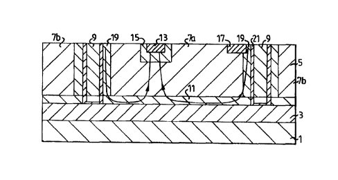
Figure 1 is a cross-sectional view of a prior art transistor made in an SOI
material.
On a substrate layer 1, lies an insulating layer 3, for example, of silicon
dioxide. On
the insulating layer there is a silicon layer 5 comprising the active
components 7a,
7b, separated by trenches 9 providing lateral insulation between the
components.
Here, only one of the active components 7a will be considered. .A buried
collector
11 is located in the silicon layer ~, adjacent to the insulating layer 3.
An emitter I3 is located at the surface of the active component 7a, surrounded
by a
base 15, in the way common in the art. A collector contact 17 is located at
the sur-
face of the active component 7a, close to the trench wall. An area 19 of the
trench
wall has been doped, to provide a low-resistance connection from the collector
contact 17 to the buried collector I 1.
CA 02310280 2000-OS-16
WU 99i26~93 PCT/SE98/02062
J
The trench 9 is normally formed according to the following:
The trench is etched in a conventional way down to the buried oxide. The
trench
wall is then doped in a conventional way, for example, with doping impurities
from
a gas source in a furnace or by high angle implantation. An oxide layer 21 is
then
grown or deposited in the trench, which is then filled with polysilicon.
Because the trench wall 19 has been doped all the way around the component 7a,
the distance between the base 15 and the trench wall 19 must be kept large to
pre
vent the formation of a too strong electric field near the base, which might
lead to
an avalanche breakdown.
Figure 2 shows the component 7a of Figure 1 seen from above, where the same
ref
erence numerals have been used to signify the same components as in Figure 1.
The
component 7a is surrounded by the trench 9. The trench wall is doped to serve
as a
IS connector between the collector contact I7 and the buried collector (not
shown). As
can be seen, the base 15 and the trench wall 19 must be kept apart by
substantially
the same distance in all directions, as shown by the arrows 23.
Figures 3A to 3F show important steps of the manufacturing process relevant to
the
production of the low collector resistance connection according to the
invention,
that is, to produce the component shown in Figure 4:
Figure 3A shows .a semiconductor component comprising a substrate layer 101.
an
insulating layer 103 and a silicon layer 10~ in which a trench has been formed
using
conventional masking and etching techniques. The component comprises an active
'
component 107 with a buried conducting layer 108. Before this stage, the
surface of
the component may be covered with an oxide and/or nitride layer (not shown).
Figure 3B shows the same semiconductor component with a layer 109 deposited
over the surface of the component. including the walls and bottom of the
trench.
CA 02310280 2000-OS-16
WO 99;26293 PCT/SE98/02062
6
The layer 109 comprises a material in which dopant ions diffuse significantly
faster
than in monocrystalline silicon, such as polysilicon, porous silicon or a
silicide.
In the case of layer 109 being a silicide, a metal is first applied over the
component,
including the walls and bottom of the trench. During a subsequent heat
treatment,
silicide is formed at the silicon-metal interface in the trench. the remaining
metal is
removed, by selectively etching the metal and not the silicide.
Figure 3C shows the same semiconductor component after the layer 109 has been
etched back from the top of the component and from the bottom of the trench,
leaving a layer 109' of the material covering the trench walls. The layer 109
does
not have to be removed from the bottom of the trench, but usually is, for
practical
reasons when anisotropic reactive ion etching is used.
Figure 3D shows the same semiconductor component after a layer 111 of oxide
has
been grown or deposited over the whole surface of the component. Instead of an
oxide, silicon nitride or another insulating material may be deposited.
In Figure 3E, the trench of the component has been filled with a suitable
material.
such as polysilicon, and an emitter 113 and a base 115 have been formed, by
mask
ing and doping steps, in the way common in the art.
In Figure 3F, collector contact 117 has been formed, by masking and doping, in
the
way common in_the art. The collector contact 117 is in contact with a part of
the
layer 109' covering the trench wall (This part 109a is shown in Figure ~).
The component is then subjected to an annealing process in a way well known in
the art. The annealing process is carried out until the dopant reaches the
buried col-
lector. The dopant should, however, not be allowed to diffuse so far as to
increase
the risk for an avalanche breakdown with doped regions. The annealing times an
CA 02310280 2000-OS-16
WD 99,':629 PCT1SE98/02062
7
temperatures depend, among other things, on the depth of the trench. Typical
values
are 1-10 hours at temperatures of approximately 800-1250C
As the diffusion velocity of the dopants in polysilicon, porous silicon and
silicide is
much higher than in monocrystalline silicon, dopants from the collector
contact 117
will diffuse through the layer i09a (see Figure 5) down to the buried
collector 108,
also diffusing slightly into the adjacent silicon of the active component, and
forming
a low-resistance connection from the collector contact to the buried collector
108.
Silicides are in themselves conductors. Therefore, the use of a silicide will
reduce
the collector resistance even more than the use of polysilicon or porous
silicon. On
the other hand, the distance between the trench wall and the base will have to
be in-
creased if the trench wall comprises a conductor. If polysilicon or porous
silicon is
used, the trench wall will be conducting only in the vicinity of the collector
contact,
so that this is the only part of the trench that have to be far away from the
base, as
shown in Figure ~.
Figure 4 is a cross-sectional view of part of the component shown in Figure
3F, to
illustrate the diffusion of dopant ions from the collector contact 117 down to
the
buried collector 108. As can be seen, the dopant diffuses from the collector
contact
I 17 through the layer 109' down to the buried collector 108 and also a short
dis-
Lance into the silicon of the active component 107. The layer 109' and the
area of
the active component 107 into which the dopant diffuses, together form a low-
resistance connection from the collector contact 1 I7 to the collector 108.
The trench formation procedure may be carried out at any point in the
manufactur-
ing process of the semiconductor, i.e. before or after the formation of the
active
components. If the trench according to the invention is foamed at an early
stage, be
fore any components are fotzled, it will also function as a fetter centre, to
capture
any metallic impurities that may be introduced in the processing. Even if made
at a
CA 02310280 2000-OS-16
VI fJ a9:2629=
PCf/SE98/0206?.
g
later stage, the trench according to the invention may still serve to reduce
leakaue
currents but will not be able to wetter impurities, or to heal damages such as
emitter
shorts, to the same degree as if it is present while the active components are
being
formed.
Figure ~ shows the active component of Figure 3F, seen from above, assuming
that
the material used in the layer 109' is not in itself conducting. In this case,
only a
portion 109a of the layer 109' and a region of the active component in the
vicinity
of this portion 109a is conducting, because of the diffusion of dopants from
the
contact 117. As can be seen, the base 11 ~ may be located very near the trench
walls
109' on all sides except the side 109a, at which the collector contact 117 is
located.
If desired, the trench wall may be placed at a distance of less than ll.un
from the
base, or even adjoining the base 11~. This makes the component significantly
smaller than the prior art component shown in Figure ?.
As mentioned in the introduction, the invention is not only applicable to
transistors
comprising a buried collector, but is equally applicable to other
semiconductors
comprising a buried conducting layer, such as diodes, thyristors, MOS or DMOS
transistors or IGBTs, when a low resistance contact to the buried conducting
layer is
desired.