Note: Descriptions are shown in the official language in which they were submitted.
CA 02310622 2000-OS-18
WO 99/08105 PC1'/US98/16527
TECHNIQUES AND SYSTEMS FOR ANALYTE DETECTION
This application claims the benefit of U.S.
provisional patent application 60/055,071, filed August 8,
1997, and U.S. provisional patent application 60/081,182,
filed April 9, 1998, both of which are incorporated herein by
reference in their entirety for all purposes.
The research carried out in this application was
supported in part by grants from the United States Army
(#DAAG55-97-1-0187), DARPA (DAAK60-97-K-9503), and the
National Science Foundation (CHE 9202583). The U.S.
government may have rights in any patent issuing from this
application.
BACKGROUND OF THE INVENTION
The field of the invention relates to sensor arrays
and techniques for the detection of analytes, and in a
specific embodiment, electronic techniques and devices for
olfaction.
Human beings have at least five senses-sight,
smell, taste, hearing, and touch. Since the earliest times,
humankind has sought techniques and devices for enhancing and
extending these senses. Many of the devices and instruments
that have been developed to extend human perception are
considered among of the most revolutionary inventions in
history. These inventions have had a profound impact on human
civilization and have led to many additional breakthroughs and
discoveries. Just a few of the many instruments developed to
extend the reach of human perception include the telescope,
microscope, stethoscope, X-rays, phonograph/radio/audio
amplifier, scanning electron microscope, night vision goggles,
and many, many others.
As would be expected, there has been considerable
interest in developing a device or instrument for the general
detection of analytes in a fluid, vacuum, air, or other
,W:I.1'.1-vll i~:W :111:', ms; r- In-.CA 02310622 2000-OS-18" - ;s.).)~4E3.~.N
:3
+~I ;) ti'.3 _> « r .
-__, : TTnjPR Fr?\ N0. . 65f10~b24c? Oct. ~ T 1ca=~ 01:41PM F
W '09910;1105 P~C'TlUS98MbS27
r"~edium. A SpeClfl.C ir..3r.:ace Cf ari d:'id.!y::e det~CtCr i8 a ce~~=
sens_ng =:ne':. or oGVro ii.e., analytas in ai=1 . It a.s v:zi;
rac.~ur_med th:a- some an'!:-ta_s like 'oas havQ a keener lens; c.,: s;ne;l
=t:an huna:~ be:.nys . 3acause of t!~_:r wros~s, " dogs ha<.-e beeZ
J ur_ili=ed to mar_f tasks =nci~:~?i :g, =o= example, =he detection of
bcr~s, :Tt~ilCs, :Y::gs, poisor. cFses, ar_d =i~.zral con=tabard; aocs a? s-o
ai:i is t":~ s~3rth and rescue of humar_s. _~e':rirss for. sen~;i7~ bmel'~
weulv: be sisezul for the -=a~zit_cnal applications ~~hzre animals ar_
used, as ;vc~l1 a3 for a nult_tud.4 ~f uses where anima's are
111 .impractical or i: apFropriace.
Moreover, a de-...yc? f:.,r t?:e er_er ai d ~~~- ~ ~ tes
3 c _....,.icn of a :a_~
has potentially many mr;e applications c~:cn a specify device fer
setaoLing sm~i? s : or e:id;llDie, r_'.~e uses f~~= a dav_ ~e for ana'_}~te
cetect_o_2 :,r:.~=ude 'he d~Caotion cf cY:emlCdl lea:a, oualit~r control
1~ .... ..~-~d rnceseinc, medi=al d_ac~ '
gnosis ar.d te3ting, fabricar.;om a.__~_d
ma: ufaC'Ll:.'e C~ COt'~mPY'C:L~? ~_ and 11'ld;lst:"~dl QOadS,
T'.."ldWTldCe'lltl~~~l
rv<j'l~ti7n, t°SCl:lc~ Or ~V3~L;dt1??CJ any' OC~Jra_1C Or andlVte 1T.
ah'd
mpdism ;e.y. , fua~., oi'~, ::ir:e; seivents) , and many ce her _
appLicatiorw. r~r_ instrument f,~= anaa_rt= ~3e=ecticn v:c~;ld be 1==ghll
de;i=able ___ indLS::r ies a; 3 applicat'_er_s such as t: a c'~emica-_ and
p=trocher-:ica1 seCtcrs, °ocd, f.ra~rance, mediCai, aut~~troti~:Y,
r.._'.itar-~, e:viror_me:ta~l, r~=alth ar: eafety, and induar air ~;,a_itJ,,
Tt:wrefore, it is dFs i=3LI2 Co de-relop tac:lr_iques anrJ devices fpx t~ a
uei_actia.~. o= a_aalytes.
An a~proach fo; sens,_aa smellA 1$ to use surface
.wcustic °.,tave (SAw) re3Griaters. Hpwe~rer, the signal transc.ucton
r~sc!:ar_is.~~ for S.~,w cevic=S 1='1'It'~Ayes rFlati~rel.r Gomplicared
clectrc nits, a..~_d are thus scrtewhat Costly. F'arthermcre, S~_w Gavices
are generally e:ctremely sensiti~~e to both pass an:d acoustic
impecar::e cha-yes, and may not be suitable for wse in all
en-: ironmer_ts. See FC'=' Wp-,t,-93 '?2n73.
Tzexefore, there is a need For techniat;.es and systems
for analyte detection, especiali;r ones that are law cost, easy to
narnfaCC'lrE, provi da rapid resporsc, an.ct pr«duae accuratj ~ _
<9_=ferantvation bec:veer_ different ana~ytea and 3~~ferer.t
,.cnc~~ntra~ions cf the sane araly~t=.
~j
AMENDED SHEET
CA 02310622 2000-OS-18
WO 99/08105 pCT/US98/16527
3
SUMMARY OF THE INVENTION
The present invention provides techniques and a
system for detecting and identifying analytes in fluids. The
present invention also provides techniques for fabricating and
manufacturing sensors to detect analytes in fluids. Analytes
may include smells, tastes, vapors, odors, gases, liquids, and
chemicals, among others. The fluid may be liquid or gaseous
in nature. In the present invention, an analyte is sensed by
sensors that output electrical signals in response to the
analyte. The electrical signals may be preprocessed by
filtering and amplification. This preprocessing may also
include adapting the sensor and electronics to the environment
in which the analyte exists. The electrical signals may be
further processed to classify and identify the analyte.
There are many possible embodiments of an analyte
detection system of the present invention. For example, the
present invention may be used to implement an electronic
olfaction system or "electronic nose." Such a system may
reveal the identification and concentration of vapors in a
manner similar to the mammalian olfactory system. .Another
embodiment for the analyte detection system of the present
invention may also be used to implement a device for tasting.
This device would function similarly to a tongue. There are
many other possible embodiments of the present invention, too
numerous to name in this application.
In one embodiment, sensors of the present invention
are fabricated using semiconductor processing techniques and
formed on a single integrated circuit. The integrated circuit
or chip may contain a plurality of sensors, each at a sensor
site. The sensor sites are formed on a substrate such as
silicon, and may be arranged in rows and columns. Structures
or other means may be constructed on the substrate to
constrain a sensor material at each sensor site. For example,
the sensor sites may be a plurality of sensor wells that could
hold the sensor material.
The sensor material applied to or formed at one
sensor site may have a different composition from the sensor
material at a different site. For example, each sensor in the
analyte detection system may have a different composition from
CA 02310622 2000-OS-18
WO 99/08105 PCTNS98/16527
4
every other sensor. For example, the sensor material may
consist of regions of a nonconductive organic insulating
material and a conductive material such as carbon black; the
composition of carbon black may vary for each sensor on the
chip. By providing a system of diverse sensors, each sensor
may have a different response characteristic for a given
analyte.
The integrated circuit may also include an
electrical connection at each sensor site to route the
electrical signals from the sensor material to other
circuitry. This circuitry may further process the electrical
signals. The circuitry may be on the same chip (on-chip) with
the sensors, or may be off the chip carrying the sensors
(off-chip), such as on a different integrated circuit. For
example, an analyte detection system of the present invention
may include two or more integrated circuits, making up an
analyte detection chipset.
In a specific embodiment of the present invention,
electronic circuitry resides on the same integrated circuit as
the sensor site. In particular, there is circuitry associated
with each sensor site, and this circuitry may be formed
beneath or interspersed with the sensor sites.
The signals from the sensors may be further
processed by classifying the response to the analyte. For
example, each analyte may have a particular "fingerprint."
The analyte may be identified based on this fingerprint. The
signal processing for the identification and classification of
the analyte may be performed by on-chip or off-chip circuitry.
For example, classification may be performed using a computer
or other instrument, among other techniques. Therefore, using
the techniques and system of the present invention, an analyte
may be distinguished and identified.
An aspect of the present invention is the use of an
array of sensors to detect analytes. A further aspect of the
present invention is the use of an integrated circuit having
an array of sensors to detect analytes. A still further
aspect of the present invention is the use of a semiconductor
process to fabricate an integrated circuit having an array of
sensors for identifying an analyte.
CA 02310622 2000-OS-18
WO 99/08105 PCTIUS98/16527
In a specific embodiment, the present invention is
an integrated circuit including a plurality of sensor sites
formed on a semiconductor substrate, each sensor site for
constraining the sensor material. The integrated circuit
5 further includes an electrical terminal formed to measure an
electrical property of the sensor material. The electrical
property may be a resistance, capacitance, inductance, or
other electrical property. The sensor material may be a
method consisting of a nonconductive organic insulating
material and a conductive material. The sensor site may be a
sensor well.
In a further embodiment, the integrated circuit of
the present invention includes an array of sensors for
detecting chemical analytes, each sensor having a first and
second output terminal. There are plurality of adaptive
electronic circuits, each circuit associated with one of the
sensors and coupled to the first and second output terminals
of the associated sensor.
To fabricate a semiconductor structure, a plurality
of layers are formed on a silicon substrate. A plurality of
wells is created in the plurality of layers. The sensor
material is deposited into each well. Further, the
composition of the sensor material in each well may be
different from the sensor material at another well on the
silicon substrate.
Other objects, features, and advantages of the
present invention will become apparent upon consideration of
the following detailed description and the accompanying
drawings, in which like reference designations represent like
features throughout the figures.
BRIEF DESCRIPTION OF THE DRAWINGS
Figure 1 shows a substrate with a number of analyte
detection integrated circuits;
Figure 2A shows a more detailed diagram of one
analyte detection integrated circuit;
Figure 2B shows a detailed view of a sensor well;
CA 02310622 2000-OS-18
WO 99/08105 ~ ~ ~ ~ ~ ~ ~ ~ ~ ~ ~'C''~/~998~1652"
~ ~ ~ ~ ~ ~ ~ ~ 1
~ ~ ~ ~ ~ ~ ~ ~ 1
~ ~ ~ ~ ~ ~ ~ ~ ~ ~ ~ 1 ~ ~ ~ ~ ~
~ ~ ~ ~ ~ ~ ~ ~
~ ~ ~ ~ ~ ~ ~ ~ ~ ~ ~ ~ ~ ~ ~
6
Figure 2C shows an embodiment of the present
invention in which a detection chip is formed with only a
single conducting layer;
Figure 3 shows how a sensor array including a
collection of different sensors may be used to identify an
analyte;
Figure 4 shows a cross section of a sensor well;
Figure 5 shows a top view of a layout of a sensor
well;
Figure 6 shows a layout of an integrated circuit
- with a number of sensor wells; -
Figure 7 shows a top view of a layout for a sensor
site, where electronic circuitry is formed beneath the sensor
site;
Figures 8A through 8F show the different stages in
a process of fabricating sensor site and depositing the sensor
material;
Figure 9 shows a cross section of an embodiment of
a sensor site formed by planarizing an insulator layer;
Figure 10 shows a cross section of another
embodiment of a sensor site;
Figure 11 shows a cross section of a further
embodiment of a sensor site;
Figure 12 shows an equivalent circuit diagram for
the case of a discontinuous film on top of a continuous
high-impedance film;
Figure 13 is a block diagram of a technique for
evaluating or measuring the capacitance of a sensor to detect
an analyte;
Figure 14 shows another embodiment for evaluating
or measuring the capacitance of a sensor element;
Figure 15 shows a layout of capacitive sensor sites
for an integrated circuit;
Figure 16 shows a unit cell;
Figure 17 shows a diagram of circuitry for reading
out data from an array of. sensors;
Figure 18 shows a diagram of an analyte defection
system;
AMEAfpEp SNEET
CA 02310622 2000-OS-18
WO 99/08105 PCT/US98/16527
7
Figure 19 shows a specific embodiment of an analyte
detection system;
FIG. 20A is a simplified block diagram of a fluid
identification apparatus that measures the capacitive effect a
fluid has on two distinct, chemically sensitive dielectric
materials and that then classifies the resulting capacitance
measurements, to determine the identity of the fluid;
FIG. 20B is a simplified block diagram of an
alternative configuration for the classification portion of
the apparatus of FIG. 20A, this alternative configuration
including preliminary signal processing of the capacitance
measurements, e.g., by linear or non-linear amplification,
attenuation, averaging, etc.;
Figure 21(A) shows an overview of sensor design;
Figure 21(B) shows an overview of sensor operation; Figure
21(C) shows an overview of system operation;
Fig 22. Cyclic voltammogram of a poly(pyrrole)-
coated platinum electrode. The electrolyte was 0.10 M
[(C4H9)4N]' [C104]- in acetonitrile, with a scan rate of 0.10 V
s-i;
Fig 23(A) shows the optical spectrum of a spin
coated poly(pyrrole) film that had been washed with methanol
to remove excess pyrrole and reduced phosphomolybdic acid.
Fig. 23(B) shows the optical spectrum of a spin-coated
poly(pyrrole) film an indium-tin-oxide after 10 potential
cycles between +0.70 and -1.00 V vs. SCE in 0.10 M [(C4H9),N]'
[C10;]~ in acetonitrile at a scan rate of 0.10 V -s-1. The
spectra were obtained in 0.10 M KC1 - HzO;
Fig. 24(A) Schematic of a sensor array showing an
enlargement of one of the modified ceramic capacitors used as
sensing elements. The response patterns generated by the
sensor array described in Table 3 are displayed for: Fig.
24(B) acetone; Fig 24(C) benzene; and Fig 24(D) ethanol;
Fig. 25., Principle component analysis of
autoscaled data from individual sensors containing different
plasticizers. (A) poly(styrene)s (B) poly (?-methyl styrene);
(C) polystyrene-acrylonitrile); (D) polystyrene-allyl
alcohol);
CA 02310622 2000-OS-18
WO 99/08105 PCT/US98/16527
8
Fig. 26(A) and 26(B). Principle component analysis
of data obtained from all sensors (Table 3). Conditions and
symbols are identical to Figs. 25(A)-25(D). Fig 26A shows
data represented in the first three principle components pcl,
pct and pc3, while Fig. 26B shows the data when represented in
pcl, pct, and pc4. A higher degree of discrimination between
some solvents could be obtained by considering the fourth
principle component as illustrated by larger separations
between chloroform, tetrahydrofuran, and isopropyl alcohol in
Fig. 268.
Fig. 27(A). Plot of acetone partial pressure (O)
as a function of the first principle component; linear least
square fit (-) between the partial pressure of acetone and the
first principle component (Pa = 8.26~pcl + 83.4, Rz - 0.989);
acetone partial pressure (+) predicted from a multi-linear
least square fit between the partial pressure of acetone and
the first three principle components (Pa = 8.26~pcl - 0.673~pc2
+ 6.25~pc3 + 83.4, RZ - 0.998). Fig. 27(B). Plot of the mole
fraction of methanol, xm, (O) in a methanol - ethanol mixture
as a function of the first principle component; linear least
square fit ( ) between xm and the first principle component
(xm = 0.112~pcl + 0.524, RZ - 0.979); x~ predicted from a
multilinear least square fit (+) between x_ and the first three
principle components (xm = 0.112~pcl - 0.0300~pc2 - 0.0444~pc3
+ 0.524, RZ - 0.987);
Fig. 28. The resistance response of a poly(N-
vinylpyrrolidone):carbon black (20 w/w~ carbon black) sensor
element to methanol, acetone, and benzene. The analyte was
introduced at t=60 s for 60 s. Each trace is normalized by
the resistance of the sensor element (approx. 125?) before
each exposure; and
Fig. 29. First three principal components for the
response of a carbon-black based sensor array with 10 element.
The non-conductive components of the carbon-black composites
used are listed in Table 3, and the resistors were 20 w/w~
carbon black.
DESCRIPTION OF THE SPECIFIC EMBODIMENTS
CA 02310622 2000-OS-18
WO 99/08105 PCT/US98/16527
9
The present invention provides techniques for the
detection and identification of analytes. These analytes may
be in fluids, which may be liquid or gaseous in nature. The
techniques of the present invention may also be used to
provide other information about analytes, including for
example, the concentration, classification, volume, flow rate,
direction of a plume trail, location of source of analyte,
gradient, and other characteristics. For example, the
techniques of the present invention may allow the
determination of the concentration of a first analyte and a
second analyte in a mixture.
A system of analyte detection of the present
invention has many applications. This system may be embodied
within analytical instruments, handheld devices, robots, and
many other devices and tools. For example, the system of the
present invention may, in a specific implementation, reside on
a single integrated circuit or multiple integrated circuits.
There are however many other ways to implement a system of the
present invention. For example, the system of the present
invention may have components which are relatively close in
proximity to another, such as being resident on the same
substrate, integrated circuit, or printed circuit (PC) board.
Alternatively, various components of the analyte detection
system may also reside in different locations, and linked by a
network or other communications link. This network may
include a local-area network, wide-area network, wireless
network, cellular phone network, optical network, the
Internet, electrical wire, and many others, and combinations
of these networks.
An example of a specific embodiment of the present
invention is an electronic system of analyte detection. In
particular, the electronic system of analyte detection may
include a plurality of sensors. Further, one sensor in the
plurality of sensors may have a different characteristic from
another sensor in the plurality. In an even further
embodiment, each sensor in the plurality of sensors may have
different characteristics from every other sensor. U.S.
Patent Number 5,571,401 discusses sensors and sensor materials
which may be used in a system of the present invention,
CA 02310622 2000-OS-18
WO 99/08105 PGT/US98/16527
although other sensors and sensor materials may also be used.
U.S. Patent Number 5,571,401 is incorporated herein by
reference in its entirety for all purposes.
A technology that has led to the proliferation of
5 modern electronics is the integrated circuit. Integrated
circuit technology may be used in an electronic analyte
detection system of the present invention. However, the
present invention is not necessarily limited to integrated
circuit technology, as there are many other technologies for
10 implementing the present invention. For example, the system
of the present invention may be practiced using discrete
electronic components assembled on a printed circuit board. A
system of the present invention may be contained within a
handheld electronic device.
Using integrated circuit technology to fabricate an
electronic analyte detection device permits relatively low
cost and high volume manufacture of such devices. Integrated
circuits are the modern marvel of today's electronic and
information age. Commonly referred to as "chips," integrated
circuits are miniaturized electronic circuits fabricated on
silicon substrates. Chips are commonplace in the electronics
market, and are the building blocks for a vast number of
electronic products used in many industries. Products using
integrated circuits include computers, computer peripherals,
consumer electronics, telecommunications and networking
equipment, and many others.
A system of the present invention may be
manufactured using integrated circuit technology. However,
the present invention is not necessarily limited to
implementations using integrated circuit technology; other
technologies may also be used. The present invention is also
not limited to electronic olfaction since a system according
to the present invention may be used to detect, identify, and
classify analytes in a variety of mediums and environments.
Figure 1 shows an implementation of the present
invention using integrated circuit technology. A substrate or
wafer 110 has a number of analyte detection chips 120.
Similar to the case with integrated circuit fabrication, many
analyte detection chips 120 may be formed on a single
CA 02310622 2000-OS-18
WO 99/08105 PC'T/US98/16527
11
substrate. There may be hundreds or thousands of such chips
on one substrate.
The substrate may be silicon, such as single
crystal silicon having a < 1 0 0 > or < 1 1 1 > orientation.
Other materials may also be used as a substrate including,
just to name a few, other semiconductive materials, other
materials suitable for the manufacture of integrated circuits,
insulators, diamond, silicon (or other semiconductor material)
over an insulator (such as sapphire), plastic, fused
substrates, and polymers.
Analyte detection chips 120 may be fabricated on
the substrate using a semiconductor process typical of the
integrated circuit industry. Successive layers of various
materials are formed and patterned on the substrate. The
layers may include, just to name a few examples, diffusion (n-
and p-type), silicon oxide, gate oxide, polysilicon, metal
(including multiple layers of metal), contact, and via. These
layers may be formed on the substrate by deposition, growth,
ion implantation, sputtering, electroplating, and other
techniques. Photoresist may be used to pattern the features
on the substrate. Features may be etched using dry or wet
etching techniques, and combinations of these in the same
process.
In one embodiment of the present invention, analyte
detection chips are fabricated using a CMOS process
technology. Many other technologies may also be used, such as
NMOS, BiCMOS, bipolar, and others.
Individual analyte detection chips are formed
adjacent to other chips on the substrate. Individual chips
are separated from each other by a scribe line 130. In many
instances, each analyte detection chip is substantially
identical to another. It is however possible to manufacture
different types or different designs of analyte detection
chips on a wafer. There may also be test die or structures on
the wafer to allow testing and evaluation of various process
parameters and properties of the analyte detection chips
during the fabrication of the wafer. Test structures may also
be formed in the scribe lines between the individual dies.
CA 02310622 2000-05-18
WO 99/08105 PCT/US98/16527
12
During the manufacture of analyte detection chips,
a sensor material is placed on the substrate. For example,
this sensor material may be deposited, coated, or otherwise
applied on the substrate. In one embodiment, the sensor
material is any material which provides an electrical response
to an analyte or odorant. For example, an electrical response
may be quantified in terms of impedance (R), inductance (L),
capacitance (C), or other electrical changes. In an
embodiment, the sensor material may be a polymer. The
material may be organic, or inorganic in other embodiments.
Further, the sensor material may consist of regions of a
nonconductive organic material and a conductive material. In
other embodiments, the sensor material may be insulating
organic films that act as capacitors, or composite films that
act as inductors. A more detailed description of some sensor
materials and their properties is discussed in U.S. Patent
Number 5,571,401. However, the present invention is not
limited to the sensor materials in U.S. Patent Number
5,571,401 since other materials may also be used.
In a specific embodiment of the present invention,
the sensor technology may involve a series of conductive
polymeric composite vapor sensors. The presence of an analyte
may be detected through a change in, for example, the
electrical resistance of a chemically sensitive carbon-based
resistor. As discussed above, changes in electrical
properties other than resistance may also be used; these
include the evaluation of capacitive and inductance changes.
Further, the sensor material may be composed of
conductor and insulator composites. This material may be
placed on the substrate in a film. The organic nonconducting
polymer of the composite absorbs the analyte (which may be a
vapor). This induces a change in the electrical properties of
the sensor material. The sensor material may also undergo
physical changes such as swelling. When the analyte is
removed, any changes in the electrical properties reverse.
For example, the resistance, capacitance, and inductance may
return to their original value. Any physical changes would
also reverse. The response of these types of sensors are
reversible over multiple analyte exposures as well as repro-
CA 02310622 2000-OS-18
WO 99/08105 PCT/US98/16527
13
ducible over a large number of trials under a variety of
ambient atmospheric conditions. Therefore, a device
fabricated using these types of sensor materials would have a
relatively long service life.
In the case of using a composite such a
nonconducting polymer and carbon black, the sensor material
will be temperature sensitive. When using temperature-
sensitive sensors, the sensor should be kept at a relatively
constant temperature to provide relatively consistent results.
For example, a temperature such as about 5° C above the
ambient should provide good results. Further, extremely high
temperatures, say, above about 100° C, should be avoided since
these temperatures would destroy the polymer sensor material
or rapidly decrease its service life. For this reason, it is
not expected that nonconducting polymer materials are to be
used in the specialized environment of extreme high
temperatures, say, from about 300° C to about 400° C or even
higher. The polymer sensor materials will be usable in the
normal temperature ranges from about 0° C to about 100° C.
Using a conductor and insulator composite for the
sensor material permits a very broad, diverse collection of
sensor materials. For example, any conducting element
including carbon blacks, metallic colloids, or organic
conducting polymers, and combinations of these, may be used as
the conductive phase of the sensors. Any organic material may
be used as the insulating phase of the sensors. Furthermore,
an advantage of these types of sensor materials is that they
do not have the stability limitations of conducting organic
polymeric materials. A conductor and insulator composite also
does not suffer the limitations from the types of substituents
or restrictions on the ranges of swelling variations that can
be obtained from backbone modification of pure organic
conducting polymers.
After processing of a substrate or wafer is
complete, the wafer is tested to determine the number and
location of the "good" die. The percentage of good die on one
wafer compared to the total number of die on the wafer is
referred to as the "yield." Individual analyte detection dies
are separated by sawing along the scribe lines. The analyte
CA 02310622 2000-OS-18
WO 99/08105 PCT/US98/16527
14
detection dies are then packaged, and may be further tested to
ensure their proper operation. These dies may be packaged in
a variety of packaging material including ceramic, epoxy,
plastic, glass, and many others. Packaged analyte detection
die may very much resemble packaged integrated circuit chips.
For some types of applications, nonporous, nonreactive
materials like ceramic may be used.
In one embodiment, the sensor material is deposited
or applied at the wafer level, before individual dies are
separated. In other embodiments, the sensor material is
applied after the dies are separated.
Figure 2A shows a more detailed diagram of an
analyte detection chip 205. In a basic embodiment, an analyte
detection chip of the present invention includes a plurality
of sensor sites 210 of sensor material. In the present
invention, the sensor material is constrained by some means at
each sensor site. There are many techniques of constraining
the sensor material at specific sites on the substrate. For
example, the sensor material may be constrained at specific
sites by surface tension. The sensor material may also be
constrained by an electrical charge, electric field, or
magnetic field. Further, the sensor material may be
constrained using structures formed by integrated circuit
processing techniques or other techniques (e. g.,
micromachining or microelectromechanical systems (MEMS)).
Examples of these structures include sensor wells, ridges,
trenches, circular structures, towers, and many structures to
constrain the sensor material at the sensor sites. These
structures may be fabricated on or in the substrate.
In the specific embodiment shown in Figures 2A and
2B, sensor wells are used to constrain the sensor materials at
the sensor sites. Figure 2B shows a more detailed view of a
single sensor well. In the typical case, the sensor material
may be deposited in the sensor wells of the analyte detection
chips at the wafer level, before the chips are separated from
the wafer. The sensor wells, however, may also be filled
after the individual chips have been separated from the wafer.
As discussed above, other techniques may be used to form the
sensor sites and constrain the sensor material, and sensor
CA 02310622 2000-OS-18
WO 99/08105 PCT/US98/16527
wells are shown.merely as an example. Other structures may be
used in a similar fashion to constrain the sensor material.
For the analyte detection chip in Figure 2A, the
sensor sites are arranged in an array having rows and columns
5 of 11 sensor sites by 11 sensor sites, for a total of 121
sensor sites. As discussed above, the sensor sites in Figure
2A are sensor wells. Sensor material will be applied at these
sensor sites which will serve as the analyte detection
sensors.
10 The analyte detection chip depicted in the figure
will have 121 sensors. In other embodiments, the analyte
detection chip may have fewer than 121 sensors. For example,
an analyte detection chip may have a two sensor sites, three
sensor sites, four sensor sites, or greater number of sensor
15 sites. An analyte detection chip may have two, three, four,
five, six, seven, or more sensors sites for sensors. The chip
may have ten to twenty, twenty to thirty, thirty to forty,
forty to fifty, and fifty to one hundred sensors. A specific
embodiment of the analyte detection chip has thirty-two sensor
sites. Even more complex analyte detection chips may have
many hundreds or thousands of sensors. For example, a chip
may have 10,000 sensors (possibly arranged in an array with
100 sensors per side).
The array of sensors may be arranged in many
possible formats, and may have an equal number of sensors per
side. The arrangement of the plurality of sensor sites may be
selected as appropriate for a particular application.
Although Figure 2A shows a square array arrangement of sensor
sites, the sensor sites may be arranged in any fashion on the
chip. For example, the plurality of sensor sites may be
arranged in an oblong or rectangular structure, triangular
structure, circular or curved structure, and many other
arrangements. An array of sensor sites may have 1 site by 10
or more sites, 2 sites by 10 or more sites, 3 sites by 10 or
more sites, 10 sites by 20 sites, or 30 by 175 sensors, just
to mention some examples. There may also be multiple arrays
or multiple groupings of sensor sites on the same substrate.
There may be two, three, four, five, or more arrays of sensors
on a single substrate.
CA 02310622 2000-OS-18
WO 99/08105 PCT/US98/16527
16
Figure 2C illustrates one embodiment of the present
invention in which a detection chip 220 is formed with only a
single conducting layer formed over a substrate 221. The
single conducting layer, typically of metal, such as aluminum
and its compounds, advantageously allows for a simple
semiconductor process. The simpler processing provides for
quicker manufacturing times and a reduced number of failure
mechanisms. On the other hand, the simpler processing creates
constraints in the layout of the chip 220 and necessarily
creates a chip with some functional simplification.
The chip 220 provides for a number of sensors 230A
and 230B around the periphery of the substrate 221. Only one
corner of the substrate 221 is shown. The sensors 230A and
230B are arranged in two rows and are representationally
illustrated by a dotted circle and two spaced-apart and
parallel line segments. The dotted circle represents sensor
material and the two line segments represent the electric
terminals by which a reaction of an electrical parameter of
the sensor material to an analyte or odorant is received.
Each terminal is connected to one of two conductive leads 225
and 226, one lead 226 connected to a common line 240, i.e., a
reference line, and the other lead 225 connected to a bonding
pad 241. The common line 240 is arranged as a annular ring
around the substrate 221 on the inside of the peripheral rows
of the sensors 221A and 221B. By a lead connection 228 to a
bonding pad 242, the voltage level of the common Line 240 is
fixed. As seen in Figure 2C, the two rows of sensors 231A and
231B are arranged in staggered fashion which allows the
optimum packing of the sensors. The dotted circle of each
sensor 230A and 230B also indicates the possible area covered
by the sensor material described previously.
This arrangement permits electrical signals from
each sensor 230 through the sensor's bonding pad 241 and the
common bonding pad 242. The signals may be derived directly
from the electrical characteristics of the sensor material or
may be signals which have been preprocessed by the electrical
circuits associated with each sensor 230, as described below.
In either case, this arrangement can be implemented by "a
single-metal layer" process, a term well understood in the
CA 02310622 2000-OS-18
WO 99/08105 PCT/US98/16527
17
semiconductor industry. Processing and layout is
advantageously straightforward. With semiconductor technology
readily available today, a chip with 32 sensors is easily
manufactured. The surface is treated with gold to assure good
contacts.
In other embodiments, a system of analyte detection
may use sensors that reside on separate substrates. For
example, the analyte detection system of the present invention
may gather analyte information from sensors in different
physical locations such as sensors located at various
positions of a production line or different rooms within a
building.
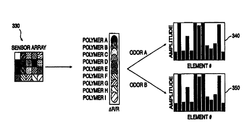
Figure 3 shows how a plurality of sensors 330 of
the present invention may be used to identify an analyte. In
an embodiment, the sensors would be formed on a substrate at
sensor sites, and these sites may be arranged in an array form
as discussed above. Each of the sensors may be incrementally
different, and each is not specifically responsive to any
particular analyte. For example, each sensor may have
essentially a different polymer composite resistance change
(listed as polymer A through polymer I) from every other
sensor. When two analytes, such as odor A and odor B, are
evaluated using the collection of sensors, the result will be
two different response patterns 340 and 350. Each analyte has
a characteristic "fingerprint." Pattern recognition
processing may then be used to identify the analytes on the
basis of these patterns.
In an embodiment of the present invention such as
shown in Figure 3, every sensor has a different composition of
sensor material from every other sensor. This may be referred
to as "sensor diversity." In other embodiments of the present
invention, however, there may be multiple sensors in a sensor
array that are the same. In other words, some groups of
sensors in this embodiment will be manufactured with exactly
the same composition, while other groups of sensors will have
a different composition. Having two or more of the same
sensors in a sensor array may serve a redundancy purpose,
which may be useful to increase the production yield.
Redundancy in sensors may be useful for increasing the service
CA 02310622 2000-OS-18
WO 99/08105 PCT/US98/16527
18
life or reliability of an analyte detection chip, especially
when used in harsh environments (e. g., industrial) or mission
critical situations (e.g., military, bomb detection, or use by
a common carrier). The techniques of the present invention
for analyte detection also apply to cases where similar
sensors exist in an array of sensors.
An aspect of the present invention is the use of a
plurality of sensors having different response characteristics
to distinguish and classify analytes: These sensors may be
formed on the same substrate. The plurality of sensors will
give a multidimensional response for use in characterizing and
classifying the analyte.
A particular sensor material may be broadly
responsive in the presence of many analytes. A response or
signal from one sensor allows detection of a change in the
composition of an analyte, but does not necessarily allow
identification of that analyte. An array of sensor elements
provides a reversible, diagnostic pattern of changes in an
electrical parameter (such as resistance, capacitance, or
inductance) upon exposure to different analytes. When a
number of sensors with diverse chemical compositions is used,
an analyte will have a particular fingerprint or signature.
Correlations between the elements of a sensor array
may require many more than two sensors to successfully
distinguish molecules in a complex environment. A greater
number of sensors generally allows the identification of a
greater number of analytes. Moreover, a greater number also
decreases the chance that two analytes will have a similar or
the same fingerprint. The sensitivity of an analyte detection
system depends in part on the number of sensors, and diversity
of the sensors. The analyte detection system of the present
invention may be related to a biological analog, the nose. It
is believed the human olfaction system has about 106 total
sensors of about 10' different types of receptors. As is well
known, dogs have a keener sense of smell than humans. A
canine's nose has about l0e sensors, which is two orders of
magnitude greater then the human nose.
Greater numbers of sensors may be useful in a
number of ways. It may be beneficial to measure the same
CA 02310622 2000-OS-18
WO 99/08105 PCT/US98/16527
19
property in many different ways due to noise limitations in a
practical system. For example, if sufficient precision could
be obtained, it might be possible to identify uniquely any
molecule merely from a 38-bit measurement using two sensors.
But in practice, it may not practical to make such precise
measurements. Hence, when using lower precision measurements,
useful information on the nature of the analyte may be
obtained by making measurements using many independent
determinations from many different sensor elements (such as in
a sensor array).
Furthermore, a limited number of sensors may be
sufficient to distinguish between a series of pure substances
that are maintained at a fixed, known concentration. However,
if the background is unknown, if mixtures are present, or if
the background gases are changing in concentration, many more
sensors may be needed simply to avoid ambiguity in
interpretation of the output signal pattern. Even more
sensors may be needed if optimal discrimination is to be
accomplished between a given target signature and a wide
possible range of background clutter. Having large numbers of
sensors also allows redundancy and provides the ability to
reject or veto the output of poorly performing sensors.
Having greater numbers of sensors may also improve
a signal-to-noise response or reduce the time required to
identify an analyte. It is possible to achieve
signal-to-noise ratio gains from averaging over a large number
of sensors during a given observation time. Therefore, with
10,000 sensors, for example, a n1~2 signal-to-noise ratio gain
would yield an effective sensitivity increase of almost two
orders of magnitude over the capabilities of 1 to 10 sensors.
Because of all of these issues, the number of
sensors to successfully sense and identity an analyte in a
practical device may rapidly multiply from a minimum value. A
main goal of array-based sensing is to insure that no two
analytes will have the same fingerprint response from the
array, and also that a given target pattern is not confused as
a mixture of other, unanticipated or unknown, background
components. Therefore, it is generally desirable to integrate
large numbers of sensors into an array structure. The present
CA 02310622 2000-OS-18
WO 99/08105 pGT/US98/16527
invention permits the manufacture of a large number of sensor
elements in a low-cost, parallel process. And, the processing
allows sensor elements to be chemically diverse.
An array of six to eight sensors is sufficient to
5 adequately distinguish between analytes. This is the case
when the electronics used with the sensors provides adequate
accuracy, such as a very precise analog-to-digital converter.
As the number of sensors increases, fewer bits of accuracy
will be required to distinguish between analytes as discussed
10 above. For example, with sixteen to twenty sensors, less
precise electronics are needed. With the integrated circuit
technology available today, one practical implementation of an
analyte detection chip has thirty-two sensors. Signals from
thirty-two sensors may be decoded and processed by electronics
15 using an analog-to-digital converter with about twenty bits of
accuracy. This is not unduly complicated or prohibitively
costly to implement. As integrated circuit technology
improves, it is expected that it will become practical to
fabricate more than thirty-two sensors on a single integrated
20 circuit, and to process the signals from these sensors.
The chemical sensor material is applied at a sensor
site. The chemical sensor material has electrical properties
that can be measured in terms of electrical parameters. These
parameters may be resistance, capacitance, or inductance. In
the presence of an analyte or odor, the chemical sensor
material will have a measurable response characteristic. A
change or pattern of changes in the electrical properties of
the sensors in sensor array may be measured to identify a
particular analyte.
By evaluating a change in, for example, the
resistance of the sensor material, an analyte detection system
of the present invention may identify an analyte. A
particular sensor may have a baseline resistance of 50K ohms
(R1). However, when the sensor is placed in the presence of
an analyte such as water vapor or hexane, the resistance of
the sensor may change to 51K ohms (R2). This change in the
resistance (i.e., (Rl - R2) . R1) relative to the baseline
resistance value may be used to identify the analyte. The
baseline resistance value is used as a reference point. The
CA 02310622 2000-OS-18
WO 99/08105 PCT/US98/16527
21
value of baseline resistance may vary depending on the
operating conditions of the sensors such as the pressure,
temperature, and humidity. The baseline resistance may also
vary because the background ambient may change. For example,
there may be background analytes which are not of interest and
should not be considered during any measurements.
Changes in electrical properties other than
resistance of the sensor material may also be measured and
similarly analyzed. Resistance has been discussed merely as
an example. A change in the capacitance or inductance of the
sensor material may be measured to identify an analyte. In
the presence of an analyte, the capacitance change of the
sensor material (which may be due to a physical swelling of
the material) may be measured.
A composition of the sensor material may determine
its response characteristic. A sensor in a first position in
the array may have a slightly different composition from
another sensor in a second position in the array. The two
sensors will give different response characteristics, and this
difference may be used to help distinguish different analytes
or odorants. For example, if a mixture of a nonconductive and
conductive polymer is used as the sensor material for an array
of sensors, the composition of the sensors may be different.
In an embodiment where carbon black is used, the carbon black
composition of each sensor may be slightly different from
other sensors in the array.
In addition to the sensor sites for constraining
the sensor material, the analyte detection chip of the present
invention may include electrical or other connections to the
sensor material at the sensor sites. For example, in the case
when resistances of the sensors are to be evaluated,
conductive layers such as metal may be used to connect with
the sensor material in a similar fashion as metal interconnect
is used in a semiconductor chip. In the case when
capacitances are to be evaluated, a conductive material may be
placed in proximity to the sensor material to allow capacitive
coupling and sensing. The electrical signals from the sensor
may then be routed to bonding pads of the analyte detection
chip. Via the bonding pads, the electrical signals from the
CA 02310622 2000-OS-18
WO 99/08105 PG"T/US98/16527
22
sensors may be connected to off-chip circuitry for further
processing and analysis.
As discussed above, in a specific embodiment of the
present invention, sensor wells constrain the sensor material.
Figure 4 shows a cross section of an implementation of a
sensor well. This sensor well may be fabricated on a silicon
substrate using a CMOS process. The sensor material will fill
and be constrained by a sensor well 410. On a silicon
substrate 415, the following layers may be patterned and used
to form sensor well 410: a field oxide (fox) layer 420, a
polysilicon (poly) layer 425, a first oxide (oxl) layer 430, a
metal-1 (M1) layer 435, a second oxide (ox2) layer 440, a
metal-2 (M2) layer 445, and a passivation or glass (GLAS)
layer. 450.
An example of a process flow for fabricating a
sensor well is as follows. An oxide layer is formed over a
silicon substrate. A metal or conductive layer is formed on
the oxide layer. The metal layer is patterned and etched.
The resulting metal is to be used as contacts for the sensor
material. An oxide layer is formed on the structure. A
sensor well is patterned and etched. The sensor material is
deposited in the sensor well and is in electrical contact with
the patterned metal layer.
In one embodiment, the sensor material is applied
to the sensor well after the sensor well is formed as a step
during the fabrication of the chip (before the formation of
the passivation layer). For example, the sensor material may
be applied at the semiconductor fabrication facility.
However, in other embodiments of the present invention, the
sensor material may be applied in a postprocessing step, after
the fabrication of the chip. For example, the sensor material
is applied after the completed wafers are received from the
semiconductor fabrication facility.
In one embodiment, the silicon substrate 415 is
about 500 microns thick. The field oxide layer 420 is about
0.6 microns thick. The polysilicon layer 425 is about 0.4
microns thick. The first oxide layer 430 is about 0.85
microns thick. The metal-1 layer 435 is about 0.6 microns
thick. The second oxide layer 440 is about 0.65 microns
CA 02310622 2000-OS-18
WO 99/08105 PCT/US98/16527
23
thick. The metal-2 layer 445 is about 1.15 microns thick.
The passivation layer 350 is about 1 micron thick.
Although the structure in Figure 4 is fabricated
using a two-layer metal process, a sensor well may be
fabricated using a single-layer metal process and also
processes having more than two layers of metal. For example,
a sensor well of the present invention may be fabricated in a
process having three, four, five, or more layers of metal.
Electrical connections 460 and 470 are formed in
the metal-1 layer to make electrical contact with the sensor
material. These electrical connections are used to route the
sensor signals to other circuitry for further processing of
sensor data. This circuitry may be on-chip or off-chip. The
metal conductor used to form connections 460 and 470 is
typically a conductive material such as gold, platinum,
aluminum, or copper. The material for the electrical
connections 460 and 470 should be selected so they are not
reactive to the sensor material. In the case when the sensor
material is applied during a postprocessing step, connections
460 and 470 will be exposed, and a conductive material such as
aluminum may easily oxidize. This may result in poor
electrical connections to the sensor material.
Good electrical contacts are more important for
some embodiments of the present invention than others. For
example, a good physical contact may be important when
measuring the resistance of the sensor material. This is
especially true in cases when the sensor material has a
relatively low resistance when compared to the contact
resistance. In other cases, such as when measuring
capacitance, connections may be made by using a capacitive
connection, where there is no physical connection between the
sensor material and the conductive material or metal.
Consequently, in such an embodiment, there would be fewer
concerns associated with oxidation of the metal connection.
The metal-1 layer may be, for example,
postprocessed or at least finished in a nonstandard integrated
circuit fashion. The surface of standard integrated circuit
metalization is normally covered by a thin, air forming,
"native" oxide layer. Aluminum, the most popular standard
CA 02310622 2000-OS-18
WO 99/08105 PCT/US98/16527
24
metal, forms aluminum oxide continuously over its surface very
quickly when exposed to air. Polymer/carbon black composite
resistors can not be taken to high temperatures nor can they
be energetically formed in other ways to break through the
"native" oxide. As such, a means for good contact to the
metal layer must be made. This could be accomplished by
chemically or physically etching the exposed electrodes and
keeping the metal-1 in an oxygen-free environment while
applying the polymer composite sensor material. More
practically, an additional layer, or multiple layer sandwich,
whose exposed layer is a noble (nonoxidizing) metal may be
deposited through any number of techniques on the surface of
metal-1. This technique could be physical vapor deposition or
chemical vapor deposition or plating amongst others. The
technique of sputtering a gold contact layer over a chromium
glue layer, followed by photo lithographically defining the
metal sandwich is especially attractive.
The circuitry receiving the sensor signals from
connections 360 and 370 may be off-chip or on-chip. The other
circuitry may include preprocessing, amplification, and
classification of the sensor data. Depending on the packaging
technology used, bonding pads may be formed along the
periphery or edges of the chip, or may be distributed inside
the chip (e. g., when using flip-chip packaging technology).
The sensor well structure of Figure 4 may be used
to constrain and allow measurement of the sensor material.
The sensor material fills or partially fills sensor well 410,
and resistance is measured using electrical connections 460
and 470.
Figure 5 shows a top view of a 200-micron by
200-micron sensor well structure. Metal is used to make
electrical connections 520 and 530 at opposite ends of the
sensor well.
Figure 6 shows a layout of a test structure with
four sensor wells 610, 620, 630, and 640. These sensor wells
are of various sizes. Specifically, sensor wells 620 and 640
are squares of 200 microns per side while sensor wells 610 and
630 are squares of 400 microns per side. Bonding pads 650
surround the four sensor wells and are electrically connected
CA 02310622 2000-OS-18
WO 99/08105 PCT/US98/16527
to the sensor wells. Two bonding pads or electrical
connections may be used to connect to a particular sensor
well. For example, pads 660 and 670 connect to the two
terminals for sensor well 620. One bonding pad or electrical
5 connection may be shared between two different sensor wells.
Figure 7 shows a further embodiment of the present
invention where electronic circuitry is formed below or
beneath the sensor site. The figure shows a top view of a
layout of the electronic devices at a sensor site. Electrical
10 contacts 710 and 715 make electrical contact between the
sensor material and electronic circuitry. In this case, the
electronic devices implement a preprocessing circuit.
More specifically, the preprocessing circuit may
include an autozeroing adaption circuit with signal
15 amplification and X-Y decoding. The individual circuit blocks
include a sensor read-out amplifier with baseline adaption
circuit 720; signal amplification circuits 730, 735, and 740;
and a row/column select and final output amplification circuit
750. In other embodiments of the present invention, however,
20 electronic circuitry for any purpose may be implemented at or
beneath the sensor site. Outputs from the electronic
circuitry may be routed to other on-chip circuitry, or
off-chip circuitry via the bonding pads.
In Figure 7, the sensor site is a 200-micron by
25 200-micron sensor well. However, as discussed above, in other
embodiments of the present invention, the sensor material may
be constrained at the sensor site using a structure or
technique other than a sensor well. Furthermore, in other
embodiments of the present invention, electronic circuitry is
not necessarily formed beneath the sensor site, and may be
placed anywhere on the same integrated circuit chip. For
example, electronic circuitry may be formed adjacent to the
sensors, or in another location on the chip. However, an
advantage of forming electronic circuitry beneath the sensors
is that the resulting layout is relatively compact.
A cross-sectional structure for the embodiment of
Figure 7 may be similar to what is shown in Figure 4 where the
electrical devices are formed using metal-1 and polysilicon
layers. To be able to form electrical devices beneath the
CA 02310622 2000-OS-18
WO 99/08105 PCT/US98/16527
26
sensor well, the second oxide layer will not be etched
through. The second oxide layer will instead form a "bottom"
for the sensor well. The metal-1 layer is used to
electrically connect to the sensor material at the sensor
site.
Figures 8A through 8F show the different stages in
the microfabricating a sensor well structure. The technique
shown in Figure 8A through 8F may be an alternative to a CMOS
semiconductor process. For example, the process may be a MEMS
or microelectrical fabrication process or other specialized
VLSI process. The process may include micromachining to form
the structures to constrain the sensor material.
The process can be self-standing (with no
underlying electronic circuits) or done in combination with
other layers underneath the sequence of layers shown added in
Figures 8A through 8F. A starting wafer or substrate is shown
in 8A. This layer is either an insulating substrate or a
starting wafer to which has been added an insulating film.
This can be either through oxidation (for a silicon substrate)
or deposition. A conductive film may be deposited onto the
insulating surface by either physical or chemical vapor
deposition methods shown in Figure 8B. The metal or
conductive film is patterned in Figure 8C leaving a pair of
electrodes. An additional insulating film is deposited in
Figure 8D and patterned to expose the electrodes of a
nonoxidized metal structure in Figure 8E. Into the well
defined by the top insulator film and between the two
electrodes in the bottom of the well, is deposited the sensor
material shown in Figure 8F.
Sensor materials of diverse compositions are
applied at the sensor sites of the chip. There are many
techniques of applying the sensor material at the sensor
sites. For example, the sensor material may be deposited at
the sensor sites by using solution spin coating or deposition
of monomers and then polymerizing them. In an embodiment
where the sensor material are polymer-based chemiresistors,
the polymer-based chemiresistors may be formed by spin- or
dip-coating substrates. with solutions or suspensions of the
chemiresistor components. Furthermore, for the case of
CA 02310622 2000-OS-18
WO 99/08105 PCT/US98/16527
27
spin-coated layers or for the case of dip-coated layers, the
need for diversity dictates there be a patterning of the first
sensor material followed by the application and patterning of
many subsequent layers. While not unfeasible, the number of
times that this process need be repeated is dictated by the
degree of diversity that is desired in the sensors.
Another technique to produce sensor sites
containing sensor materials with diverse compositions is to
deposit the sensor material serially in time. This will
involve making a first deposition at a site which contains a
distinct chemical composition from the second, from the third,
and so forth.
A still further technique for applying the sensor
material is to use microjet or ink jet technology. Ink jet
technology is increasingly being used in the fabrication of
devices. With such technology, it is possible to fabricate
polymeric structures on the order of 100 microns and arrays of
these structures with packing densities of greater than 15,000
per square centimeter. Microjets may be useful tools in
fabricating large arrays of miniaturized sensors for analyte
detection.
For example, to fabricate a diverse set of sensors
on a substrate, a continuous jet system may be employed
because the composition of the "ink" (e. g., the sensor
material which may be a chemical polymer) can be continuously
changed. This allows for the fabrication of sensor material
films with variable composition from a limited feedstock of
monomers or polymers as desired. The monomers delivered into
the sensor sites would be polymerized in situ in a subsequent
step through exposure to gamma irradiation, to a suitable free
radical catalyst or by exposure to light. In this fashion, it
will be possible to prepare libraries of thousands of
different polymers from uncorrelated monomeric precursors, and
to rapidly evaluate their efficacy in distinguishing the
analytes of concern.
When using microjet technology, it is important to
prevent the ink jet nozzles from clogging. It- is desirable
for the particle size of the ink be smaller than the nozzle
size. In a specific embodiment, microjet technology may be
CA 02310622 2000-OS-18
WO 99/08105 PCT/US98/16527
28
used to apply polymers with carbon black. In fact, classic
black inks (such as India ink) are carbon black suspensions.
The nozzle size of commercial ink jets is generally greater
than ten microns. Since a stable carbon black suspension with
particle sizes of less than one micron may be formed, it is
possible to fabricate carbon black suspensions compatible with
microjet technology.
In addition to standard electrostatically
controlled continuous flow or drop-on-demand systems, other
options are available. Mechanically controlled ink jets with
larger nozzles, essentially small spray guns, may also be
used. Another microjet technology is the compound ink jet.
With such a device, a jet of the so-called primary fluid
emerges from a 10- to 20-micron orifice submerged in a
so-called secondary fluid. The resulting jet consists of both
fluids, and can be manipulated as in a standard
electrostatically controlled continuous ink jet. Compound
jets can utilize carbon black based inks, such as India ink,
as a secondary fluid since the reservoir for this fluid can be
of arbitrary size.
Although the above techniques for manufacturing are
highly desirable for some applications, in other applications
such as those that include a large numbers of sensor elements
in the array, another embodiment of the present invention may
be more desirable. Figs. 7G shows a cross section of a
portion of an integrated circuit 700 according to this further
embodiment. An advantage of this method is that it is highly
flexible, and might be used with any number of different base
integrated circuit processes. For example, this method is
especially useful for those applications which require
addressing the array a bit at a time, because many such
addressable array architectures have been developed in silicon
technology, and this technique allows one to make use of these
previously developed infrastructures.
Referring to Figure 9, a plurality of semiconductor
devices 905 are formed within a substrate 910 by any
conventional VLSI fabrication processes, as is well-known in
the art. Conductors 915 are formed in a conductive layer to
interconnect semiconductor devices 905 and to provide routing
CA 02310622 2000-OS-18
WO 99/08105 PCT/US98/16527
29
to the various sensors. Semiconductor devices 905 and
conductors 915 are interconnected to form the various
electronics on integrated circuit 900. For example, they may
form the electronics for addressing and activating an array of
sensor elements. Conductors 915 may be, for example,
polysilicon, metal (e. g., aluminum or copper), or other
conductive layers. In an embodiment of the invention that
measures the change of resistance of a sensor, two layers of
metal (not shown) are used for a bias to be generated and
current measured at a given X-Y location in the array. Since
the information that provides a signal is the change in the
resistance of a node, the access lines can be relatively high
impedance without causing any serious loss of signal or
inducing much additional Johnson noise. Hence, the
polysilicon layer, available in every CMOS technology, is
usable. In a typical scenario, with a hundred squares of
resistance at 10 ohms per square, a polysilicon line might be
on the order 1000 ohms of fixed resistance in series with the
signal resistor.
An insulator layer 920 of SiOz, SiOxN4, or other
insulating material is formed above semiconductor device 910.
Insulator layer 920 electrically isolates semiconductor
devices 910 and conductors 915. Contacts 730 are formed
within insulator layer 920 to allow electrical connections to
conductors 915, and may be formed of a variety of conductive
materials such as tungsten or other refractory metals.
Although only one contact 930 is shown in Figure 9 for
simplicity, it will be recognized that each sensor may have
more than one contact 930 connected to it, for example, to use
the contact as a resistive element between two conductors.
After contacts 930 and insulator layer 920 are
formed, integrated circuit 900 is planarized to provide a
substantially flat surface. The planarization may be
accomplished, for example, using chemical-mechanical
processing (CMP), a technique well known in the art of
integrated circuit processing. By so doing, contacts 930 are
exposed. Contacts 930 having exposed metal may be covered
with an optional noble metal coating 935 through physical
CA 02310622 2000-OS-18
WO 99!08105 PCT/US98/16527
vapor deposition, chemical vapor deposition, or plating
techniques to provide an optimal electrical contact.
A polymer forming a sensor 940 of the type
described above is deposited on contact 915 (or noble metal
5 coating 935 if provided). In the combinatorial approach to
making sensors devices, thousands of sensors 940 might be made
by varying the composition of two, three, four, or more
different types of polymers. A flat surface for this purpose
would be desirable.
10 If for some reason a sensor well becomes necessary
to physically separate individual sensors, beyond the
electrical separation offered by the addressable contacts 930,
then a second insulator layer 950 may be provided with opening
for sensors 940. Insulator layer 950 is preferably Teflon° (a
15 trademark of E.I. DuPont de Nemours and Company),
Teflon°-like material, or other fluoropolymer, although other
insulators may be used. In the case that postprocessing is
needed, a flat topography on integrated circuit 900 from the
planarization step is highly desirable.
20 Particularly in the case of an integrated circuit,
a premium is placed on the amount of real estate taken up by
sensors 940. To conserve real estate area, it is desirable to
place the sensors above semiconductor devices 905 that make up
the electronics for the array. This effectively doubles the
25 use of the real estate. Because of their size, sensors 940
can become the determinant of the size of the chip if each
sensor 940 has to be isolated physically from every other
sensor 940. In this case, the dilution of the solution used
to cast sensor 940 is desired to be as high as possible. The
30 thinner the film the finer the degree to which it can be
patterned or physically localized by other means.
In a preferred embodiment of integrated circuit
900, sensor 940 should be as thin as possible without
destroying its electrical properties. If the desired
thickness of the polymer film becomes smaller than the
conductive particle size, solution casting becomes
impractical. Thus, in an alternate embodiment of the present
invention, sensors 940 are formed by putting the conductive
particles down and then coating the conductive particles with
CA 02310622 2000-OS-18
WO 99/08105 PCT/US98/16527
31
the polymer films through a vapor deposition process. In some
embodiments, these films may be made with no polymer at all,
and yet still be sensitive to analytes. By putting down the
conductive particles first and then coating them with a thin
film of polymer, one could have an effective active film
arbitrarily thin supported by the larger conductive particles
in a porous configuration. Put another way, instead of casting
a polymer film with included conductive particles, sensor 940
is formed by making a porous particle film with polymer
coating the particles. This improves the response much faster
and the lateral dimensions determined by the localization of a
polymer vapor deposition.
Another response time enhancement is to make sensor
940 with an inert or sacrificial particle filler which is
either very permeable or removable after deposition. While
this does not change the thickness parameter positively, in
some cases it is a simpler way to achieve the response time
benefits of the spongy film detailed above with the
application techniques that are in use today.
Figure 10 is a cross-sectional diagram showing
another example of a sensor element of the present invention
created by another method. This technique also benefits from
the planarized integrated circuit described with respect to
Figure 9. In this embodiment, semiconductor devices 1005,
conductors 1010, and contacts 1030 are formed and the
integrated circuit is planarized as described above, and
optional noble metal coating 1035 is formed above contact
1030. Then, micromachining techniques are used to form high,
hurdle-like structures 1060. By this technique, it is
possible to place contacts 1030 very close together on the
surface of the integrated circuit. A polymer film 1065 is
deposited onto hurdle-like structure 1060 with a thickness
that may be determined by the surface tension or wetting
properties of the polymer, solvent conductive particle
mixture, rather than the volume in the drop or dispensed
amount. This allows the sensor to be thinner, the response
faster and the silicon area to be reduced.
Figure 11 shows another embodiment of the present
invention that may take advantage of the planarization
CA 02310622 2000-OS-18
WO 99/08105
PCTNS98/16527
32
technique described above with respect to Figure 9. Above the
planarized insulator layer 1120, a very high impedance film
1180 is placed across semiconductor devices (not shown in
Figure 11) that form the array. Chemisensitive sensors 1185
are deposited right on top of high impedance film 1180 forming
a distributed parallel resistor. This allows working in a
domain of thinness where the actual signal generating film
does not need to be continuous. Even if short segments
change, the terminal resistances within the array would be
impacted.
In particular, the equivalent circuit for the case
of a discontinuous film on top of a continuous high-impedance
film is shown in Figure 12. The high impedance film is
represented by leg B in the drawing or as a continuous
resistor. Leg A of the drawing shows a group of variable
resistors that are in parallel with the underlying resistor.
When the resistors A1 through A3 change in response to the
presence of an analyte, the resistance between points 1 and 2
of the drawing change even though the changing film may not be
continuous.
Figure 13 is a block diagram of an embodiment of
the present invention that measures a capacitance of the
sensor material to determine the presence of an analyte.
While Figure 13 shows only a single pair of sensors, the
circuitry may also be expanded to include an array of sensors
or an array of pairs of sensors. Each sensor in the array may
include a different type of sensor material from other sensors
as described above.
Capacitance may be measured in a variety of ways.
30. Figure 13 depicts one such method. However, other circuitry
for measuring capacitance may be substituted for the circuitry
shown. In the embodiment shown, two sensors 1310 and 1320 are
provided. Sensors 1310 and 1320 are sensors formed
substantially identical to one another. However, sensor 1410
is exposed such that analytes may penetrate the sensor
material and cause it to expand. On the other hand, sensor
1320 is covered by an insulator layer so that it will not be
affected by analytes. As such, sensor 1320 is a reference
sensor, and its capacitance can be compared with the
CA 02310622 2000-OS-18
WO 99/08105 PCT/US98/16527
33
capacitance of sensor 1310 to determine if sensor 1320 has
expanded due to the presence of an analyte.
One technique of evaluating the capacitors of the
sensors involves frequency generators. Frequency generators
1330 and 1332 are coupled to sensors 1310 and 1320,
respectively, through contacts 1340 and 1342. Frequency
generators 1330 and 1332 output an oscillating signal at a
particular frequency, and receive back return signals fl and
f2. Return signals fl and f2 may be phase-shifted or
frequency shifted, depending upon the capacitance of the
sensor. Thus, if sensor 1310 has not expanded, the
capacitance is the same as that of sensor 1320 and fl is the
same as f2. In the case when an analyte is present, the
capacitance of sensor 1320 is greater, and thus fl is not the
same as f2. In fact, the difference between fl and f2 may be
used to determine the change in capacitance.
The return signals fl and f2 are input to a
discriminator mixer 1350. Discriminator mixers are well known
in the electrical arts, and in particular for example, in the
design of phase locked loops. Mixer 1350 receives two
frequencies, and outputs a DC output that is zero if the
frequencies are the same, and nonzero if the frequencies are
different. The greater the frequency difference, the higher
the value of the DC output. Thus, if the output of mixer 1350
is zero, then the capacitance of the two sensors are the same,
and no analyte is present; if the magnitude of the output is
nonzero, then an analyte is present, and may be identified by
the value of the DC output.
Of course, other capacitance measuring circuitry
may also be used. For example, two similar adjacent sensors
may be formed such that they have room to expand in a sideways
direction. Each of the two sensors are coupled to a different
conductive trace, and the sensors are coupled through the
conductive trace to a capacitance measuring circuit. When no
analyte is present, the sensors have a certain separation,
that is known, and thus has a known capacitance. When an
analyte is present, the sensors expand and the distance
between them shortens causing the capacitance to change. By
CA 02310622 2000-OS-18
WO 99/08105 PCT/US98/16527
34
measuring the change in capacitance, the presence of the
analyte may be determined.
Figure 14 shows another embodiment of the present
invention for measuring the capacitance of a sensor element.
Two similar sensors 1410 and 1420 are provided. In a specific
embodiment, sensors 1410 and 1420 are substantially identical.
A capacitive measuring device 1430 coupled to sensor 1410 by
two conductors 1440 and 1442 through contacts or otherwise.
The capacitive measuring device is any device capable of
determining a capacitance of sensor 1410. Similarly, a second
capacitance measuring device is coupled to sensor 1420 through
two conductors 1460 and 1462. Sensor 1420 is isolated from
exposure to analytes, while sensor 1410 may be exposed to
them. A comparator 1470 compares the capacitances measured
from the two sensors 1410 and 1420. These values may be
analyzed by various techniques described above or otherwise.
Figure 15 shows an integrated circuit layout that
may be used for the circuit shown in Figure 14. Conductors
1540 and 1542 are interdigitated on the integrated circuit.
These conductors are associated with one capacitor. Sensor
1510 is formed above the interdigitated conductors.
Similarly, sensor 1520 is formed above interdigitated
conductors 1560 and 1562. These conductors are associated
with another capacitor.
Figure 16 shows a "unit cell" 1610 for a sensor of
the analyte detection chip of the present invention. To form
a plurality of sensors, unit cell 1610 may be repeated as many
times as desired. For example, for an analyte detection chip
with ten sensors, the unit cell is repeated ten times. For an
analyte detection chip with thirty sensors, the unit cell is
repeated thirty times. For a chip with 100 sensors, the unit
cell is repeated 100 times. For a chip with "n" sensors, the
unit cell is repeated at least "n" times.
As discussed above, a basic embodiment of unit cell
1610 includes sensor 1620 by itself. Electrical connections
from the unit cell will be connected to other electronic
circuitry, on-chip or off-chip, for further processing. For
example, in a two-chip analyte detection chipset solution, a
first of the chips may contain a plurality of sensors 1620 and
CA 02310622 2000-OS-18
WO 99/08105 pCT/tJS98/16527
their respective electrical connections. A second of the
chips may be electrically coupled to sensors 1620 to process
the signals from the sensors on the first chip.
A more highly integrated embodiment of unit cell
5 1610 includes sensor 1620 and electronics 1630, both on the
same chip or substrate. Electronics 1630 may be formed
beneath the sensor site of sensor 1620, as was described for
Figure 4 above. Electronics 1630 are electrically coupled to
sensor 1620 by connections 1640 and 1650. Electronics 1630
10 processes the signals from the sensor. The processing
includes amplification or filtering, or both. An output 1660
of the electronics may be coupled to other circuitry 1670 for
even further processing. For example, the other circuitry may
be off-chip for classifying the analyte.
15 Figure 17 shows an embodiment of circuitry for
reading out a sensor array. As the number of wires grows with
the number of sensors in an array, the practicality of using
an inactive array is reduced. It becomes desirable as the
number of sensors in the array approaches about 100 to reduce
20 the wiring complexity with the addition of a matrix addressing
scheme shown in Figure 17. The array of chemically sensitive
sensors is shown in this embodiment as variable resistors,
each connected between a row bias line and a column read line.
A row and a column multiplexer are to "sample" the sensor data
25 in a scheme somewhat like to scanning a television picture. A
row address is translated into the application of bias (i.e.,
iBias) to one row, and the column address is translated into
the closure of a column read switch switching the output to a
load resistor that is at the input of an analog-to-digital
30 (A/D) converter whose output is in turn fed to the controller
of the system. It should be clear that the functions of bias
and read could be reversed and that other configurations of
lead resistors, included buffering circuitry and many other
functions could be included.
35 In an embodiment of an array of sensor cells, there
may also be dummy rows and columns of sensors, which is a row
or column of sensors is formed but not used functionally as
are active rows and columns of sensors. For example, at row
and column edges of the array, dummy rows and columns of
CA 02310622 2000-OS-18
WO 99/08105 PCT/US98/16527
36
sensors may be formed. These dummy rows and columns of
sensors may be used to ensure the active interior row and
columns of sensors are relatively uniform, since sensors at
the edge may exhibit some edge effects by not having a similar
number of adjacent sensors as for the interior sensors.
Dummy rows and columns (not necessarily at edges of
the array) may also be used in a redundancy scheme when these
are activated, possibly by laser programming or programming of
nonvolatile or one-time programmable memory elements such as
Flash, EEPROM, EPROM, or antifuse cells. These dummy row and
columns may be used in the place of other rows and columns
that are or have become defective. For example, a redundancy
scheme may help improve the yield of good die, or increase the
service life of an analyte detection chip.
Figure 18 shows a block diagram of an analyte
detection system. The block diagram for a discrete system
that has been developed are shown in the analyte detection
system block diagram and system design. Any full analyte
sampling system should include a means for sampling the
analyte of interest. This could be as simple as a stick to
attach the sensors and a means for holding it in the vicinity
of a vapor of interest, or as complex as a network of pumps
and valves sequencing through a complex sampling routine.
Once the analyte has been presented to the array of chemically
sensitive transducers, the signals are processed and presented
to an A/D converter. The pattern of response across the array
is then compared to a stored pattern of response and an
identification can be made through any number of possible
input output channels as simple as wires to a control system
or as complex as a visual display system.
Figure 19 shows a block diagram of a specific
embodiment of an analyte system of the present invention. A
particular embodiment of such a system is shown in the block
diagram of a system that has been implemented in a discrete
design. There are thirty-two sensors (e. g., chemiresistive
sensors) organized in four groups of eight. The signals are
buffered, and each bank of eight sensor signals is then fed
through an 8-to-1 analog multiplexer to an A/D that has an
additional 4-to-1 multiplexer internal to it. The data is
CA 02310622 2000-OS-18
WO 99/08105 PCT/US98/16527
37
streamed out of the A/D converter in a serial bit stream to a
central processing unit (CPU). The CPU may be a computer.
The CPU additionally is interfaced to a heater control system.
As the chemically sensitive sensors are also temperature
dependant, controlling the temperature in the system
eliminates one source of noise. The data is stored by the CPU
in random access memory (RAM) or in another storage media such
as magnetic disk. The measurements can be compared to a
learned pattern of response previously stored and the CPU can
calculate the best match and report the result through the LCD
panel display.
As the number of sensors grows beyond thirty-two,
the number of connections can become impractical to make with
solder or other physical attachment processes. More of the
block diagram will then be integrated onto a chip since the
wiring connections inside and integrated circuit are very
reliable. As the number of sensors approaches 100, it makes
economic sense to integrate a matrix measurement scheme on the
same substrate as the sensors. As the number of sensors grows
even further, the A/D converter can become overtaxed and more
than one makes sense to keep the system throughput in the
range of one second where the flow system time constant
becomes the limitation to overall system response. As the
number of sensors grows to an even larger number, the A/D
technology needs to be changed to either a large array of
slower A/Ds or a faster variety of converter or both. With
an array of A/D converters on the chip a digital multiplexer
needs to be added to funnel the outputs through to the CPU.
As the number of sensor elements climbs to the millions, some
condensation of the data needs to take place within the array
itself.
CA 02310622 2000-OS-18
WO 99108105 PCT/US98/16527
38
The field of the invention is electrical sensors for
detecting analytes in fluids.
There is considerable interest in developing sensors that
act as analogs of the mammalian olfactory system (1-2). This
system is thought to utilize probabilistic repertoires of many
different receptors to recognize a single odorant (3-4). In such
a configuration, the burden of recognition is not on highly
specific receptors, as in the traditional "lock-and-key"
molecular recognition approach to chemical sensing, but lies
instead on the distributed pattern processing of the olfactory
bulb and the brain (5-6).
Prior attempts to produce a broadly responsive sensor
array have exploited heated metal oxide thin film resistors (7-
9), polymer sorption layers on the surfaces of acoustic wave
resonators (10-11), arrays of electrochemical detectors (12-14),
or conductive polymers (15-16). Arrays of metal oxide thin film
resistors, typically based on SnOz films that have been coated
with various catalysts, yield distinct, diagnostic responses for
several vapors (7-9). However, due to the lack of understanding
of catalyst function, Sn02 arrays do not allow deliberate chemical
control of the response of elements in the arrays nor
reproducibility of response from array to array. Surface
acoustic wave resonators are extremely sensitive to both mass and
acoustic impedance changes of the coatings in array elements, but
the signal transduction mechanism involves somewhat complicated
electronics, requiring frequency measurement to 1 Hz while
sustaining a 100 MHz Rayleigh wave in the crystal (10-11).
Attempts have been made to construct sensors with conducting
polymer elements that have been grown electrochemically through
nominally identical polymer films and coatings (15-18).
It is an object herein to provide a broadly responsive
analyte detection sensor array based on a variety of
"chemiresistor" elements. Such elements are simply prepared and
are readily modified chemically to respond to a broad range of
analytes. In addition, these sensors yield a rapid, low power,
do electrical signal in response to the fluid of interest, and
CA 02310622 2000-OS-18
WO 99/08105 PCTlUS98/16527
39
their signals are readily integrated with software or hardware-
based neural networks for purposes of analyte identification.
Pearce et a1. (1993) Analyst 118:371-377 and Gardner et al.
(1994) Sensors and Actuators B I8-19:240-243 describe
polypyrrole-based sensor arrays for monitoring beer flavor.
Shurmer (1990) US Patent No. 4,907,441, describes general sensor
arrays with particular electrical circuitry.
The invention provides methods, apparatuses and expert
systems for detecting analytes in fluids. The apparatuses
include a chemical sensor comprising first and second conductive
elements (e.g., electrical leads) electrically coupled to a
chemically sensitive resistor which provides an electrical path
between the conductive elements. The resistor comprises a
plurality of alternating nonconductive regions (comprising a
nonconductive organic polymer) and conductive regions (comprising
a conductive material). The electrical path between the first
and second conductive elements is transverse to (i.e., passes
through) said plurality of alternating nonconductive and
conductive regions. In use, the resistor provides a difference
in resistance between the conductive elements when contacted with
a fluid comprising a chemical analyte at a first concentration,
than when contacted with a fluid comprising the chemical analyte
at a second different concentration.
The electrical path through any given nonconductive region
is typically on the order of 100 angstroms in length, providing a
resistance of on the order of 100 mS2 across the region.
Variability in chemical sensitivity from sensor to sensor is
conveniently provided by qualitatively or quantitatively varying
the composition of the conductive and/or nonconductive regions.
For example, in one embodiment, the conductive material in each
resistor is held constant (e. g., the same conductive material
such as polypyrrole) while the nonconductive organic polymer
varies between resistors (e.g., different plastics such as
polystyrene).
Arrays of such sensors are constructed with at least two
sensors having different chemically sensitive resistors providing
dissimilar differences in resistance. An electronic nose for
CA 02310622 2000-OS-18
WO 99/08105 PCTNS98/16527
detecting an analyte in a fluid may be constructed by using such
arrays in conjunction with an electrical measuring device
electrically connected to the conductive elements of each sensor.
Such electronic noses may incorporate a variety of additional
5 components including means for monitoring the temporal response
of each sensor, assembling and analyzing sensor data to determine
analyte identity, etc. Methods of making and using the disclosed
sensors, arrays and electronic noses are also provided.
The invention provides sensor arrays for detecting an
10 analyte in a fluid for use in conjunction with an electrical
measuring apparatus. These arrays comprise a plurality of
compositionally different chemical sensors. Each sensor
comprises at least first and second conductive leads electrically
coupled to and separated by a chemically sensitive resistor. The
15 leads may be any convenient conductive material, usually a metal,
and may be interdigitized to maximize signal-to-noise strength.
The remainder of this discussion addresses an embodiment
where the electrical property of interest for the chemical sensor
material is resistance. However, it is also recognized that the
20 chemical sensor material has other electrical properties
including capacitance and inductance. The sensor material
exhibits a swelling phenomenon that may be measured by changes in
any electrical property such as resistance, capacitance, or
inductance, or combinations of these properties. For example, as
25 discussed above, in other embodiments of the present invention,
detecting analytes may be accomplished by evaluating a
capacitance of the sensor material.
The resistor comprises a plurality of alternating
nonconductive and conductive regions transverse to the electrical
30 path between the conductive leads. Generally, the resistors are
fabricated by blending a conductive material with a nonconductive
organic polymer such that the electrically conductive path
between the leads coupled to the resistor is interrupted by gaps
of non-conductive organic polymer material. For example, in a
35 colloid, suspension or dispersion of particulate conductive
material in a matrix of nonconductive organic polymer material,
the matrix regions separating the particles provide the gaps.
CA 02310622 2000-OS-18
WO 99/08105 PCTNS98/16527
41
The nonconductive gaps range in path length from about 10 to
1,000 angstroms, usually on the order of 100 angstroms providing
individual resistance of about 10 to 1,000 mS2, usually on the
order of 100 mf2, across each gap. The path length and resistance
of a given gap is not constant but rather is believed to change
as the nonconductive organic polymer of the region absorbs,
adsorbs or imbibes an analyte. Accordingly the dynamic aggregate
resistance provided by these gaps in a given resistor is a
function of analyte permeation of the nonconductive regions. In
some embodiments, the conductive material may also contribute to
the dynamic aggregate resistance as a function of analyte
permeation (e. g., when the conductive material is a conductive
organic polymer such as polyprryole).
A wide variety of conductive materials and nonconductive
organic polymer materials can be used. Table 1 provides
exemplary conductive materials for use in resistor fabrication;
mixtures, such as of those listed, may also be used. Table 2
provides exemplary nonconductive organic polymer materials;
blends and copolymers, such as of the polymers listed here, may
also be used. Combinations, concentrations, blend
stoichiometries, percolation thresholds, etc. are readily
determined empirically by fabricating and screening prototype
resistors (chemiresistors) as described below.
CA 02310622 2000-OS-18
WO 99/08105 PC'fNS98/16527
42
Table 1.
Major Class , Examples
Organic Conductors conducting polymers
(poly(anilines),
poly(thiophenes),
poly(pyrroles),
poly(acetylenes), etc.)),
carbonaceous materials (carbon
blacks, graphite, coke, Cso,
etc.), charge transfer
complexes
(tetramethylparaphenylenediami
ne-chloranile, alkali metal
tetracyanoquinodimethane
complexes, tetrathiofulvalene
halide complexes, etc.), etc.
Inorganic Conductors metals and metal alloys (Ag,
Au, Cu, Pt, AuCu alloy, etc.),
highly doped semiconductors
(Si, GaAs, InP, MoSz, Ti02,
etc.), conductive metal oxides
(In,03, SnOz, NaxPt,04, etc.
) ,
superconductors (YBa2Cu,0"
T12Ba2Ca2Cu,Olo, etc. ) , etc.
Mixed inorganic/organic Tetracyanoplatinate complexes,
Conductors Iridium halocarbonyl
complexes, stacked macrocyclic
complexes, etc.
CA 02310622 2000-OS-18
WO 99108105 PCTNS98/16527
43
Table 2.
Major Class Examples
Main-chain carbon poly(dienes), poly(alkenes),
polymers poly(acrylics),
poly(methacrylics),
polyvinyl ethers),
polyvinyl thioethers),
polyvinyl alcohols),
polyvinyl ketones),
polyvinyl halides),
polyvinyl nitriles),
polyvinyl esters),
poly(styrenes),
poly(arylenes), etc.
Main-chain acyclic poly(oxides),
heteroatom polymers poly(carbonates),
poly(esters),
poly(anhydrides),
poly(urethanes),
poly(sulfonates),
poly(siloxanes),
poly(sulfides),
poly(thioesters),
poly(sulfones),
poly(sulfonamides),
poly(amides), poly(ureas),
poly(phosphazenes),
poly(silanes),
poly(silazanes), etc.
Main-chain poly(furan tetracarboxylic
Heterocyclic polymers acid diimides),
poly(benzoxazoles),
poly(oxadiazoles),
poly(benzothiazinophenothiaz
fines), poly(benzothiazoles),
CA 02310622 2000-OS-18
PCTNS98/16527
WO 99/08105
44
poly(pyrazinoquinoxalines),
poly(pyromellitimides),
poly(quinoxalines),
poly(benzimidazoles),
poly(oxindoles),
poly(oxoisoindolines),
poly(dioxoisoindolines),
poly(triazines),
poly(pyridazines),
poly(piperazines),
poly(pyridines),
poly(piperidines),
poly(triazoles),
poly(pyrazoles),
poly(pyrrolidines),
poly(carboranes),
poly(oxabicyclononanes),
poly(dibenzofurans),
poly(phthalides),
poly(acetals) ,
poly(anhydrides),
carbohydrates, etc.
The chemiresistors can be fabricated by many techniques such
as, but not limited to, solution casting, suspension casting, and
mechanical mixing. In general, solution cast routes are
advantageous because they provide homogeneous structures and ease
of processing. With solution cast routes, resistor elements may
be easily fabricated by spin, spray or dip coating. Since all
elements of the resistor must be soluble, however, solution cast
routes are somewhat limited in their applicability. Suspension
casting still provides the possibility of spin, spray or dip
coating but more heterogeneous structures than with solution
casting are expected. With mechanical mixing, there are no
solubility restrictions since it involves only the physical
mixing of the resistor components, but device fabrication is more
difficult since spin, spray and dip coating are no longer
CA 02310622 2000-OS-18
WO 99/08105 PC"TNS98/16527
possible. A more detailed discussion of each of these follows.
For systems where both the conducting and non-conducting
media or their reaction precursors are soluble in a common
solvent, the chemiresistors can be fabricated by solution
5 casting. The oxidation of pyrrole by phosphomolybdic acid
presented herein represents such a system. In this reaction, the
phosphomolybdic acid and pyrrole are dissolved in tetrahydrofuran
(THF) and polymerization occurs upon solvent evaporation. This
allows for THF soluble non-conductive polymers to be dissolved
10 into this reaction mixture thereby allowing the blend to be
formed in a single step upon solvent evaporation. The choice of
non-conductive polymers in this route is, of course, limited to
those that are soluble in the reaction media. For the
poly(pyrrole) case described above, preliminary reactions were
15 performed in THF, but this reaction should be generalizable to
other non-aqueous solvent such as acetonitrile or ether. A
variety of permutations on this scheme are possible for other
conducting polymers. Some of these are listed below. Certain
conducting polymers, such as substituted poly-
20 (cyclooctatetraenes), are soluble in their undoped, non-
conducting state in solvents such as THF or acetonitrile.
Consequently, the blends between the undoped polymer and
plasticizing polymer can be formed from solution casting. After
which, the doping procedure (exposure to IZ vapor, for instance)
25 can be performed on the blend to render the substituted
poly(cyclooctatetraene) conductive. Again, the choice of non-
conductive polymers is limited to those that are soluble in the
solvents that the undoped conducting polymer is soluble in and to
those stable to the doping reaction. Certain conducting polymers
30 can also be synthesized via a soluble precursor polymer. In
these cases, blends between the precursor polymer and the non-
conducting polymer can first be formed followed by chemical
reaction to convert the precursor polymer into the desired
conducting polymer. For instance polyp-phenylene vinylene) can
35 be synthesized through a soluble sulfonium precursor. Blends
between this sulfonium precursor and the non-conductive polymer
can be formed by solution casting. After which, the blend can be
CA 02310622 2000-OS-18
WO 99/08105 PCTNS98/16527
46
subjected to thermal treatment under vacuum to convert the
sulfonium precursor to the desired polyp-phenylene vinylene).
In suspension casting, one or more of the components of the
resistor is suspended and the others dissolved in a common
solvent. Suspension casting is a rather general technique
applicable to a wide range of species, such as carbon blacks or
colloidal metals, which can be suspended in solvents by vigorous
mixing or sonication. In one application of suspension casting,
the non-conductive polymer is dissolved in an appropriate solvent
(such as THF, acetonitrile, water, etc.). Colloidal silver is
then suspended in this solution and the resulting mixture is used
to dip coat electrodes.
Mechanical mixing is suitable for all of the conductive/non-
conductive combinations possible. In this technique, the
materials are physically mixed in a ball-mill or other mixing
device. For instance, carbon black . non-conductive polymer
composites are readily made by ball-milling. When the non-
conductive polymer can be melted or significantly softened
without decomposition, mechanical mixing at elevated temperature
can improve the mixing process. Alternatively, composite
fabrication can sometimes be improved by several sequential heat
and mix steps.
Once fabricated, the individual elements can be optimized
for a particular application by varying their chemical make up
and morphologies. The chemical nature of the resistors
determines to which analytes they will respond and their ability
to distinguish different analytes. The relative ratio of
conductive to insulating components determines the magnitude of
the response since the resistance of the elements becomes more
sensitive to sorbed molecules as the percolation threshold is
approached. The film morphology is also important in determining
response characteristics. For instance, thin films respond more
quickly to analytes than do thick ones. Hence, with an empirical
catalogue of information on chemically diverse sensors made with
varying ratios of insulating to conducting components and by
differing fabrication routes, sensors can be chosen that are
appropriate for the analytes expected in a particular
CA 02310622 2000-OS-18
WO 99/08105 PCTNS98/16527
47
application, their concentrations, and the desired response
times. Further optimization can then be performed in an
iterative fashion as feedback on the performance of an array
under particular conditions becomes available.
The resistor may itself form a substrate for attaching the
lead or the resistor. For example, the structural rigidity of
the resistors may be enhanced through a variety of techniques:
chemical or radiation cross-linking of polymer components
(dicumyl peroxide radical cross-linking, W-radiation cross-
linking of poly(olefins), sulfur cross-linking of rubbers, e-beam
cross-linking of Nylon, etc.), the incorporation of polymers or
other materials into the resistors to enhance physical properties
(for instance, the incorporation of a high molecular weight, high
transition metal (Tm) polymers), the incorporation of the
resistor elements into supporting matrices such as clays or
polymer networks (forming the resistor blends within poly-
(methylmethacrylate) networks or within the lamellae of
montmorillonite, for instance), etc. In another embodiment, the
resister is deposited as a surface layer on a solid matrix which
provides means for supporting the leads. Typically, the matrix
is a chemically inert, non-conductive substrate such as a glass
or ceramic.
Sensor arrays particularly well-suited to scaled up
production are fabricated using integrated circuit (IC) design
technologies. For example, the chemiresistors can easily be
integrated onto the front end of a simple amplifier interfaced to
an A/D converter to efficiently feed the data stream directly
into a neural network software or hardware analysis section.
Micro-fabrication techniques can integrate the chemiresistors
directly onto a micrci-chip which contains the circuitry for
analogue signal conditioning/processing and then data analysis.
This provides for the production of millions of incrementally
different sensor elements in a single manufacturing step using
ink-jet technology. Controlled compositional gradients in the
chemiresistor elements of a sensor array can be induced in a
method analogous to how a color ink-jet printer deposits and
mixes multiple colors. However, in this case rather than
CA 02310622 2000-05-18
WO 99/08105 PCTNS98/16527
48
multiple colors, a plurality of different polymers in solution
which can be deposited are used. A sensor array of a million
distinct elements only requires a 1 cm x 1 cm sized chip
employing lithography at the 10 ~m feature level, which is within
the capacity of conventional commercial processing and deposition
methods. This technology permits the production of sensitive,
small-sized, stand-alone chemical sensors.
Preferred sensor arrays have a predetermined inter-sensor
variation in the structure or composition of the nonconductive
organic polymer regions. The variation may be quantitative
and/or qualitative. For example, the concentration of the
nonconductive organic polymer in the blend can be varied across
sensors. Alternatively, a variety of different organic polymers
may be used in different sensors. An electronic nose for
detecting an analyte in a fluid is fabricated by electrically
coupling the sensor leads of an array of compositionally
different sensors to an electrical measuring device. The device
measures changes in resistivity at each sensor of the array,
preferably simultaneously and preferably over time. Frequently,
the device includes signal processing means and is used in
conjunction with a computer and data structure for comparing a
given response profile to a structure-response profile database
for qualitative and quantitative analysis. Typically such a nose
comprises at least ten, usually at least 100, and often at least
1000 different sensors though with mass deposition fabrication
techniques described herein or otherwise known in the art, arrays
of on the order of at least 106 sensors are readily produced.
In operation, each resistor provides a first electrical
resistance between its conductive leads when the resistor is
contacted with a first fluid comprising a chemical analyte at a
first concentration, and a second electrical resistance between
its conductive leads when the resistor is contacted with a second
fluid comprising the same chemical analyte at a second different
concentration. The fluids may be liquid or gaseous in nature.
The first and second fluids may reflect samples from two
different environments, a change in the concentration of an
analyte in a fluid sampled at two time points, a sample and a
CA 02310622 2000-OS-18
WO 99/08105 PCTNS98l16527
49
negative control, etc. The sensor array necessarily comprises
sensors which respond differently to a change in an analyte
concentration, i.e., the difference between the first and second
electrical resistance of one sensor is different from the
difference between the first second electrical resistance of
another sensor.
In a preferred embodiment, the temporal response of each
sensor (resistance as a function of time) is recorded. The
temporal response of each sensor may be normalized to a maximum
percent increase and percent decrease in resistance which
produces a response pattern associated with the exposure of the
analyte. By iterative profiling of known analytes, a structure-
function database correlating analytes and response profiles is
generated. Unknown analyte may then be characterized or
identified using response pattern comparison and recognition
algorithms. Accordingly, analyte detection systems comprising
sensor arrays, an electrical measuring devise for detecting
resistance across each chemiresistor, a computer, a data
structure of sensor array response, profiles, and a comparison
algorithm are provided. In another embodiment, the electrical
measuring device is an integrated cicuit comprising neural
network-based hardware and a digital-analog converter (DAC)
multiplexed to each sensor, or a plurality of DACs, each
connected to different sensor(s).
A wide variety of analytes and fluids may be analyzed by the
disclosed sensors, arrays and noses so long as the subject
analyte is capable generating a differential response across a
plurality of sensors of the array. Analyte applications include
broad ranges of chemical classes such as organics such as
alkanes, alkenes, alkynes, dienes, alicyclic hydrocarbons,
arenes, alcohols, ethers, ketones, aldehydes, carbonyls,
carbanions, polynuclear aromatics and derivatives of such
organics, e.g., halide derivatives, etc., biomolecules such as
sugars, isoprenes and isoprenoids, fatty acids and derivatives,
etc. Accordingly, commercial applications of the sensors, arrays
and noses include environmental toxicology and remediation,
biomedicine, materials quality control, food and agricultural
CA 02310622 2000-OS-18
WO 99/08105 PC'TNS98/16527
products monitoring, etc.
The general method for using the disclosed sensors, arrays
and electronic noses, for detecting the presence of an analyte in
a fluid involves resistively sensing the presence of an analyte
5 in a fluid with a chemical sensor comprising first and second
conductive leads electrically coupled to and separated by a
chemically sensitive resistor as described above by measuring a
first resistance between the conductive leads when the resistor
is contacted with a first fluid comprising an analyte at a first
10 concentration and a second different resistance when the resistor
is contacted with a second fluid comprising the analyte at a
second different concentration.
The following examples are offered by way of illustration
and not by way of limitation.
15 Polymer Synthesis. Poly(pyrrole) films used for
conductivity, electrochemical, and optical measurements were
prepared by injecting equal volumes of Nz-purged solutions of
pyrrole (1.50 mmoles in 4.0 ml dry tetrahydrofuran) and
phosphomolybdic acid (0.75 mmoles in 4.0 ml tetrahydrofuran) into
20 a N~-purged test tube. Once the two solutions were mixed, the
yellow phosphomolybdic acid solution turned dark green, with no
observable precipitation for several hours. This solution was
used for film preparation within an hour of mixing.
Sensor Fabrication. Plasticized poly(pyrrole) sensors were
25 made by mixing two solutions, one of which contained 0.29 mmoles
pyrrole in 5.0 ml tetrahydrofuran, with the other containing 0.25
mmoles phosphomolybdic acid and 30 mg of plasticizer in 5.0 ml of
tetrahydrofuran. The mixture of these two solutions resulted in
a w:w ratio of pyrrole to plasticizer of 2:3. An inexpensive,
30 quick method for crating the chemiresistor array elements was
accomplished by effecting a cross sectional cut through
commercial 22 nF ceramic capacitors (Kemet Electronics
Corporation). Mechanical slices through these capacitors
revealed a series of interdigitated metal lines (25% Ag:75% Pt),
35 separated by 15 Vim, that could be readily coated with conducting
polymer. The monomer - plasticizer - oxidant solutions were then
used to dip coat interdigitated electrodes in order to provide a
CA 02310622 2000-OS-18
WO 99/08105 PC'TNS98I16527
51
robust electrical contact to the polymerized organic films.
After polymerization was complete, the film was insoluble and was
rinsed with solvent (tetrahydrofuran or methanol) to remove
residual phosphomolybdic acid and unreacted monomer. The sensors
were then connected to a commercial bus strip, with the
resistances of the various "chemiresistor" elements readily
monitored by use of a multiplexing digital ohmmeter.
Instrumentation. Optical spectra were obtained on a Hewlett
Packard 8452A spectrophotometer, interfaced to an IBM XT.
Electrochemical experiments were performed using a Princeton
Applied Research Inc. 173 potentiostat/175 universal programmer.
All electrochemical experiments were performed with a Pt flag
auxiliary and a saturated calomel reference electrode (SCE).
Spin-coating was performed on a Headway Research Inc. photoresist
spin coater. Film thicknesses were determined with a Dektak
Model 3030 profilometer. Conductivity measurements were
performed with an osmium-tipped four point probe (Alessi
Instruments Inc., tip spacing = 0.050", tip radii = 0.010").
Transient resistance measurements were made with a conventional
multimeter (Fluke Inc., "Hydra Data Logger" Meter).
Principle Component Analysis and Multi-linear Least Square
Fits. A data set obtained from a single exposure of the array to
an odorant produced a set of descriptors (i.e., resistances), di.
The data obtained from multiple exposures thus produced a data
matrix D where each row, designated by j, consisted of n
descriptors describing a single member of the data set (i.e., a
single exposure to an odor). Since the baseline resistance and
the relative changes in resistance varied among sensors, the data
matrix was autoscaled before further processing (19). In this
preprocessing technique, all the data associated with a single
descriptor (i.e., a column in the data matrix) were centered
around zero with unit standard deviation
(1) d,; =(d; -d;)~~;
where d; is the mean value for descriptor i and ai is the
corresponding standard deviation.
Principle component analysis (19) was performed to determine
CA 02310622 2000-OS-18
WO 99/08105 PCTNS98/16527
52
linear combinations of the data such that the maximum variance
[defined as the square of the standard deviation] between the
members of the data set was obtained in n mutually orthogonal
dimensions. The linear combinations of the data resulted in the
largest variance [or separation] between the members of the data
set in the first principle component (pcl) and produced
decreasing magnitudes of variance from the second to the n'h
principle component (pct - pcn). The coefficients required to
transform the autoscaled data into principle component space (by
linear combination) were determined by multiplying the data
matrix, D, by its transpose, DT (i.e., diagnolizing the matrix)
(19)
(2) R = DT~D
This operation produced the correlation matrix, R whose
diagonal elements were unity and whose off-diagonal elements were
the correlation coefficients of the data. The total variance in
the data was thus given by the sum of the diagonal elements in R.
The n eigenvalues, and the corresponding n eigenvectors, were
then determined for R. Each eigenvector contained a set of n
coefficients which were used to transform the data by linear
combination into one of its n principle components. The
corresponding eigenvalue yielded the fraction of the total
variance that was contained in that principle component. This
operation produced a principle component matrix, P, which had the
same dimensions as the original data matrix. Under these
conditions, each row of the matrix P was still associated with a
particular odor and each column was associated with a particular
principle component.
Since the values in the principle component space had no
physical meaning, it was useful to express the results of the
principle component analysis in terms of physical parameters such
as partial pressure and mole fraction. This was achieved via a
multi-linear. least square fit between the principle component
values and the corresponding parameter of interest. A multi-
linear least square fit resulted in a linear combination of the
principle components which yielded the best fit to the
corresponding parameter value. Fits were achieved by appending a
CA 02310622 2000-OS-18
WO 99/08105 PCTNS98/16527
53
column with each entry being unity to the principle component
matrix P, with each row, j, corresponding to a different
parameter value (e. g., partial pressure), v~, contained in vector
V. The coefficients for the best multi-linear fit between the
principle components and parameter of interest were obtained by
the following matrix operation
(3) C = (PT~P)'~~PT~V
where C was a vector containing the coefficients for the
linear combination.
A key to our ability to fabricate chemically diverse sensing
elements was the preparation of processable, air stable films of
electrically conducting organic polymers. This was achieved
through the controlled chemical oxidation of pyrrole (PY) using
phosphomolybdic acid (H,PMo120,0) (20 in tetrahydrofuran:
PY-SPY'++e
2PY'+ --~ PY2 + 2H+ ( 5 )
H3PMo~20ao + 2e + 2H+ -> HSPMo~20ao ( 6 >
The redox-driven or electrochemically-induced polymerization
of pyrrole has been explored previously, but this process
typically yields insoluble, intractable deposits of poly(pyrrole)
as the product (21). Our approach was to use low concentrations
of the H,PMolZO,o oxidant (E° - +0.36 V vs. SCE) (20) . Since the
electrochemical potential of PY;'/PY is more positive (E° _ +1.30
V vs . SCE ) ( 22 ) than that Of H,PMolaO,a/HSPMol,O,o. the equi 1 ibrium
concentration of PY+~, and thus the rate of polymerization, was
relatively low in dilute solutions (0.19 M PY, 0.09 M H,PMolZOao)
However, it has been shown that the oxidation potential of
pyrrole oligomers decreases from +1.20 V to +0.55 to +0.26 V vs.
SCE as the number of units increase from one to two to three, and
that the oxidation potential of bulk poly(pyrrole) occurs at -
0.10 V vs. SCE (23). As a result, oxidation of pyrrole trimers
by phosphomolybdic acid is expected to be thermodynamically
favorable. This allowed processing of the monomer-oxidant
CA 02310622 2000-OS-18
WO 99/08105 PCTIUS98/16527
54
solution (i.e., spin coating, dip coating, introduction of
plasticizers, etc.), after which time polymerization to form thin
films was simply effected by evaporation of the solvent. The do
electrical conductivity of poly(pyrrole) films formed by this
method on glass slides, after rinsing the films with methanol to
remove excess phosphomolybdic acid and/or monomer, was on the
order of 15 - 30 S-cml for films ranging from 40 - 100 nm in
thickness.
The poly(pyrrole) films produced in this work exhibited
excellent electrochemical and optical properties. For example,
Fig. 42 shows the cyclic voltammetric behavior of a chemically
polymerized poly(pyrrole) film following ten cycles from -1.00 V
to +0.70 V vs. SCE. The cathodic wave at -0.40 V corresponded
to the reduction of poly(pyrrole) to its neutral, nonconducting
state, and the anodic wave at -0.20 V corresponded to the
reoxidation of poly(pyrrole) to its conducting state (24). The
lack of additional faradaic current, which would result from the
oxidation and reduction of phosphomolybdic acid in the film,
suggests that the Keggin structure of phosphomolybdic acid was
not present in the film anions (25) and implies that MoO,z-, or
other anions, served as the poly(pyrrole) counterions in the
polymerized films.
Fig 23A shows the optical spectrum of a processed
polypyrrole film that had been spin-coated on glass and then
rinsed with methanol. The single absorption maximum was
characteristic of a highly oxidized poly(pyrrole) (26), and the
absorption band at 4.0 eV was characteristic of an interband
transition between the conduction and valence bands. The lack of
other bands in this energy range was evidence for the presence of
bipolaron states (see Fig. 23A), as have been observed in highly
oxidized poly(pyrrole) (26). By cycling the film in 0.10 M
[ (C,H9),N] ' [C104] - - acetonitrile and then recording the optical
spectra in 0.10 M KCl - HZO, it was possible to observe optical
transitions characteristic of polaron states in oxidized
poly(pyrrole) (see Fig. 23B). The polaron states have been
reported to produce three optical transitions (26), which were
observed at 2.0, 2.9, and 4.1 eV in Fig. 23B. Upon reduction of
CA 02310622 2000-OS-18
WO 99/08105 PC"fNS98/16527
the film (c.f. Fig 23B), an increased intensity and a blue shift
in the 2.9 eV band was observed, as expected for the ~-~~*
transition associated with the pyrrole units contained in the
polymer backbone (27).
5 As described in the experimental section, various
plasticizers were introduced into the polymer films (Table 3).
Table 3. Plasticizers used in
array elements*
Sensor Plasticizes
1 None
2 none**
3 polystyrene)
4 polystyrene)
5 polystyrene)
6 poly(a-methyl styrene)
7 poly(styrene-
acrylonitrile)
8 polystyrene-malefic
anydride)
9 polystyrene-allyl
alcohol)
10 polyvinyl pyrrolidone)
11 polyvinyl phenol)
12 polyvinyl butral)
13 polyvinyl acetate)
14 poly(carbonate)
10 *Sensors contained 2:3 (w: w) ratio of pyrrole to plasticizes.
**Film not rinsed to remove excess phosphomolybdic acid.
These inclusions allowed chemical control over the binding
15 properties and electrical conductivity of the resulting
plasticized polymers. Sensor arrays consisted of as many as 14
different elements, with each element synthesized to produce a
distinct chemical composition, and thus a distinct sensor
CA 02310622 2000-OS-18
WO 99/08105 PCTNS98/16527
56
response, for its polymer film. The resistance, R, of each film-
coated individual sensor was automatically recorded before,
during, and after exposure to various odorants. A typical trial
consisted of a 60 sec rest period in which the sensors were
exposed to flowing air (3.0 liter-min-1), a 60 sec exposure to a
mixture of air (3.0 liter-min-1) and air that had been saturated
with solvent (0.5 - 3.5 liter-min-1), and then a 240 sec exposure
to air (3.0 liter-min-1) .
In an initial processing of the data, presented in this
paper, the only information used was the maximum amplitude of the
resistance change divided by the initial resistance, ~R""x/R;, of
each individual sensor element. Most of the sensors exhibited
either increases or decreases in resistance upon exposure to
different vapors, as expected from changes in the polymer
properties upon exposure to different types chemicals (17-18).
However, in some cases, sensors displayed an initial decrease
followed by an increase in resistance in response to a test odor.
Since the resistance of each sensor could increase and/or
decrease relative to its initial value, two values of OR"~X/Ri were
reported for each sensor. The source of the bi-directional
behavior of some sensor/odor pairs has not yet been studied in
detail, but in most cases this behavior arose from the presence
of water (which by itself induced rapid decreases in the film
resistance) in the reagent-grade solvents used to generate the
test odors of this study. The observed behavior in response to
these air-exposed, water-containing test solvents was
reproducible and reversible on a given sensor array, and the
environment was representative of many practical odor sensing
applications in which air and water would not be readily
excluded.
Figs. 4B-4D depict representative examples of sensor
amplitude responses of a sensor array (see, Table 3). In this
experiment, data were recorded for three separate exposures to
vapors of acetone, benzene, and ethanol flowing in air. The
response patterns generated by the sensor array described in
Table 3 are displayed for: (B) acetone; (C) benzene; and (D)
ethanol. The sensor response was defined as the maximum percent
CA 02310622 2000-OS-18
WO 99/08105 PCTNS98/16527
57
increase and decrease of the resistance divided by the initial
resistance (gray bar and black bar, respectively) of each sensor
upon exposure to solvent vapor. In many cases sensors exhibited
reproducible increases and decreases in resistance. An exposure
consisted of: (i) a 60 sec rest period in which the sensors were
exposed to flowing air (3.0 liter-min-1); (ii) a 60 sec exposure
to a mixture of air (3.0 liter-min-1) and air that had been
saturated with solvent (0.5 liter-min-1); and (iii) a 240 sec
exposure to air (3.0 liter-min-1). It is readily apparent that
these odorants each produced a distinctive response on the sensor
array. In additional experiments, a total of 8 separate vapors
(acetone, benzene, chloroform, ethanol, isopropyl alcohol,
methanol, tetrahydrofuran, and ethyl acetate), chosen to span a
range of chemical and physical characteristics, were evaluated
over a five-day period on a 14-element sensor array (Table 3).
As discussed below, each odorant could be clearly and
reproducibly identified from the others using this sensor
apparatus.
Principle component analysis (19) was used to simplify
presentation of the data and to quantify the distinguishing
abilities of individual sensors and of the array as a whole. In
this approach, linear combinations of the OR"~X/Ri data for the
elements in the array were constructed such that the maximum
variance (defined as the square of the standard deviation) was
contained in the fewest mutually orthogonal dimensions. This
allowed representation of most of the information contained in
data sets shown in Figs. 24B-24D in two (or three) dimensions.
The resulting clustering, or lack thereof, of like exposure data
in the new dimensional space was used as a measure of the
distinguishing ability, and of the reproducibility, of the sensor
array.
In order to illustrate the variation in sensor response of
individual sensors that resulted from changes in the plasticizing
polymer, principle component analysis was performed on the
individual, isolated responses of each of the 14 individual
sensor elements in a typical array (Fig. 25). Data were obtained
from multiple exposures to acetone (a), benzene (b), chloroform
CA 02310622 2000-05-18
WO 99/08105 PCT/US98/16527
58
(c), ethanol (e), isopropyl alcohol (i), methanol (m),
tetrahydrofuran (t), or ethyl acetate (Q) over a period of five
days with the test vapors exposed to the array in various
sequences. The numbers of the figures refer to the sensor
elements described in Table 3. The units along the axes indicate
the amplitude of the principle component that was used to
describe the particular data set for an odor. The black regions
indicate clusters corresponding to a single solvent which could
be distinguished from all others; gray regions highlight data of
solvents whose signals overlapped with others around it.
Exposure conditions were identical to those in Fig. 24.
Since each individual sensor produced two data values,
principle component analysis of these responses resulted in only
two orthogonal principal components; pct and pct. As an example
' 15 of the selectivity exhibited by an individual sensor element, the
sensor designated as number 5 in Fig. 25 (which was plasticized
with poly(styrene)) confused acetone with chloroform, isopropyl
alcohol, and tetrahydrofuran. It also confused benzene with
ethyl acetate, while easily distinguishing ethanol and methanol
from all other solvents. Changing the plasticizer to poly (a-
methyl styrene) (sensor number 6 in Fig. 25) had little effect on
the spatial distribution of the responses with respect to one
another and with respect to the origin. Thus, as expected, a
rather slight chemical modification of the plasticizer had little
effect on the relative variance of the eight test odorants. In
contrast, the addition of a cyano group to the plasticizer, in
the form of polystyrene-acrylonitrile), (sensor number 7 in Fig.
25), resulted in a larger contribution to the overall variance by
benzene and chloroform, while decreasing the contribution of
ethanol. Changing the substituent group in the plasticizer to a
hydrogen bonding acid (poly(styrene-allyl alcohol), sensor number
9 in Fig. 25) increased the contribution of acetone to the
overall variance while having little effect on the other odors,
with the exception of confusing methanol and ethanol. These
results suggest that the behavior of the sensors can be
systematically altered by varying the chemical composition of the
plasticizing polymer.
CA 02310622 2000-OS-18
WO 99108105 PCTNS98/16527
59
Fig. 26 shows the principle component analysis for all 14
sensors described in Table 3 and Figs. 24 and 25. When the
solvents were projected into a three dimensional odor space (Fig.
26A or 26B), all eight solvents were easily distinguished with
the specific array discussed herein. Detection of an individual
test odor, based only on the criterion of observing -1% ~Rmnx/R;
values for all elements in the array, was readily accomplished at
the parts per thousand level with no control over the temperature
or humidity of the flowing air. Further increases in sensitivity
are likely after a thorough utilization of the temporal
components of the OR",ax/R; data as well as a more complete
characterization of the noise in the array.
We have also investigated the suitability of this sensor
array for identifying the components of certain test mixtures.
This task is greatly simplified if the array exhibits a
predictable signal response as the concentration of a given
odorant is varied, and if the responses of various individual
odors are additive (i.e., if superposition is maintained). When
a 19-element sensor array was exposed to a number, n, of
different acetone concentrations in air, the (CH3)ZCO
concentration was semi-quantitatively predicted from the first
principle component. This was evident from a good linear least
square fit through the first three principle components.
The same sensor array was also able to resolve the
components in various test methanol-ethanol mixtures (29). As
shown in Fig. 278, a linear relationship was observed between the
first principle component and the mole fraction of methanol in
the liquid phase, ~", in a CH,OH-C2HSOH mixture, demonstrating that
superposition held for this mixture/sensor array combination.
Furthermore, although the components in the mixture could be
predicted fairly accurately from just the first principle
component, an increase in the accuracy could be achieved using a
multi-linear least square fit through the first three principle
components . This relationship held for CH,OH/ (CH30H + C2HSOH)
ratios of 0 to 1.0 in air-saturated solutions of this vapor
mixture. The conducting polymer-based sensor arrays could
therefore not only distinguish between pure test vapors, but also
CA 02310622 2000-OS-18
WO 99108105 PCTNS98/16527
allowed analysis of concentrations of odorants as well as
analysis of binary mixtures of vapors.
In summary, the results presented herein advance the area of
analyte sensor design. A relatively simple array design, using
5 only a multiplexed low-power do electrical resistance readout
signal, has been shown to readily distinguish between various
test odorants. Such conducting polymer-based arrays are simple
to construct and modify, and afford an opportunity to effect
chemical control over the response pattern of a vapor. For
10 example, by increasing the ratio of plasticizer to conducting
polymer, it is possible to approach the percolation threshold, at
which point the conductivity exhibits a very sensitive response
to the presence of the sorbed molecules. Furthermore, producing
thinner films will afford the opportunity to obtain decreased
15 response times, and increasing the number of plasticizing
polymers and polymer backbone motifs will likely result in
increased diversity among sensors. This type of polymer-based
array is chemically flexible, is simple to fabricate, modify, and
analyze, and utilizes a low power do resistance readout signal
20 transduction path to convert chemical data into electrical
signals. It provides a new approach to broadly-responsive odor
sensors for fundamental and applied investigations of chemical
mimics for the mammalian sense of smell. Such systems are useful
for evaluating the generality of neural network algorithms
25 developed to understand how the mammalian olfactory system
identifies the directionality, concentration, and identity of
various odors.
Fabrication and Testing of Carbon Black-based Sensor Arrays.
30 Sensor Fabrication. Individual sensor elements were
fabricated in the following manner. Each non-conductive polymer
(80 mg, see Table 4) was dissolved in 6 ml of THF.
CA 02310622 2000-OS-18
WO 99/08105 PCT/US98/16527
61
Table 4.
Sensor # Non-Conductive Polymer
1 poly(4-vinyl phenol)
2 polystyrene - ally) alcohol)
3 poly(a-methyl styrene)
4 polyvinyl chloride - vinyl acetate)
polyvinyl acetate)
6 poly(N-vinyl pyrrolidone)
7 poly(bisphenol A carbonate)
8 polystyrene)
9 polystyrene-malefic anhydride)
poly(sulfone)
5 Then, 20 mg of carbon black (BP 2000, Cabot Corp.) were
suspended with vigorous mixing. Interdigitated electrodes (the
cleaved capacitors previously described) were then dipped into
this mixture and the solvent allowed to evaporate. A series of
such sensor elements with differing non-conductive polymers were
10 fabricated and incorporated into a commercial bus strip which
allowed the chemiresistors to be easily monitored with a
multiplexing ohmmeter.
Sensor Array Testing. To evaluate the performance of the
carbon-black based sensors, arrays with as many as 20 elements
were exposed to a series of analytes. A sensor exposure
consisted of (1) a 60 second exposure to flowing air (6 liter
min-1), (2) a 60 second exposure to a mixture of air (6 liter
min-1) and air that had been saturated with the analyte (0.5
liter min-1), (3) a five minute recovery period during which the
sensor array was exposed to flowing air (6 liter min-1). The
CA 02310622 2000-OS-18
WO 99/08105 62 PCT/US98/16527
resistance of the elements were monitored during exposure, and
depending on the thickness and chemical make-up of the film,
resistance changes as large as 250% could be observed in response
to an analyte. In one experiment, a 10 element sensor array
consisting carbon-black composites formed with a series of non-
conductive polymers (see Table 4) was exposed to acetone,
benzene, chloroform, ethanol, hexane, methanol, and toluene over
a two day period. A total of 58 exposures to these analytes were
performed in this time period. In all cases, resistance changes
in response to the analytes were positive, and with the exception
of acetone, reversible (see Figure 28). The maximum positive
deviations were then subjected to principal component analysis in
a manner analogous to that described for the poly(pyrrole) based
sensor. Figure 29 shows the results of the principal component
analysis for the entire 10-element array. With the exception of
overlap between toluene with benzene, the analytes were
distinguished from one and other.
Cited References: 1. Lundstr8m et al. (1991) Nature 352:47-
50; 2. Shurmer and Gardner (1992) Sens: Act. B 8:1-11; 3. Reed
(1992) Neuron 8:205-209; 4. Lancet and Ben-Airie (1993) Curr.
Biol. 3:668-674; 5.
Kauer (1991) TINS 14:79-85; 6. DeVries and Baylor (1993)
Cell 10(S):139-149; 7. Gardner et al. (1991) Sens. Act. B 4:117-
121; 8. Gardner et al. (1991) Sens. Act. B 6:71-75; 9. Corcoran
et al. (1993) Sens. Act. B 15:32-37; 10.
Grate and Abraham (1991) Sens. Act. B 3:85-111; 11. Grate et
al. (1993) Anal. Chem. 65:1868-1881; 12. Stetter et al. (1986)
Anal. Chem. 58:860-866; 13. Stetter et al. (1990) Sens. Act. B
1:43-47; 14. Stetter et al. (1993) Anal. Chem. Acta 284:1-11; 15.
Pearce et al. (1993) Analyst 118:371-377; 16. Shurmer et al.
(1991) Sens. Act. B 4:29-33; 17. Topart and Josowicz (1992) J.
Phys. Chem. 96:7824-7830; 18. Charlesworth et al. (1993) J. Phys.
Chem. 97:5418-5423; 19. Hecht (1990) Mathematics in Chemistry: An
Introduction to Modern Methods (Prentice Hall, Englewood Cliffs,
NJ); 20. Pope (1983) Heteropoly and Isopoly Oxometalates
(Springer-Verlag, New York), chap. 4; 21. Salmon et al. (1982) J.
Polym. Sci., Polyrn. Lett. 20:187-193; 22. Andrieux et al. (1990)
CA 02310622 2000-OS-18
WO 99/08105 63 PCTNS98/16527
J. Am. Chem. Soc. 112:2439-2440; 23. Diaz et al. (1981) J.
Electroanal. Chem. 121:355-361; 24. Kanazawa et al. (1981) Synth.
Met. 4:119-130; 25. Bidan et al. (1988) J. Electroanal. Chem.
251:297-306; 26. Kaufman et al. (1984) Phys. Rev. Lett. 53:1005-
1008; 27. Yakushi et al. (1983) J. Chem. Phys. 79:4774-4778; and
Morris et al. (1942) Can. J. Res. H 20:207-211.
All publications and patent applications cited in this
specification are herein incorporated by reference as if each
individual publication or patent application were specifically
and individually indicated to be incorporated by reference.
A sensor array for detecting an analyte in a fluid for
use in conjunction with an electrical measuring apparatus, said
array comprising at least first and second chemical sensors each
comprising: at least first and second conductive leads suitable
for electrical connection to the electrical measuring apparatus
and electrically coupled to a chemically sensitive resistor
comprising a plurality of alternating nonconductive regions
comprising a nonconductive organic polymer and conductive regions
comprising a conductive material compositionally different than
said nonconductive organic polymer, said resistor providing an
electrical path between said conductive leads and through said
regions, a first electrical resistance between said conductive
leads when said resistor is contacted with a first fluid
comprising a chemical analyte at a first concentration, and a
second electrical resistance between said conductive leads when
said resistor is contacted with a second fluid comprising said
chemical analyte at a second different concentration the
difference between said first electrical resistance and said
second electrical resistance of said first chemical sensor being
different from the difference between said first electrical
resistance and said second electrical resistance of said second
chemical sensor.
A sensor array where said plurality of nonconductive
regions of said first chemical sensor is different from said
plurality of nonconductive regions of said second chemical
sensor.
A sensor array wherein said nonconductive organic polymer
CA 02310622 2000-OS-18
WO 99/08105 PCTNS98/16527
64
of said first chemical sensor is qualitatively different from
said nonconductive organic polymer of said second chemical
sensor.
A sensor array wherein said conductive material is an
inorganic conductor.
A system for detecting an analyte in a fluid, said system
comprising: at least first and second chemical sensors each
comprising at least first and second conductive leads
, electrically coupled to a chemically sensitive resistor
comprising a plurality of alternating nonconductive regions
comprising a nonconductive organic polymer and conductive regions
comprising a conductive material compositionally different than
said nonconductive organic polymer, said resistor providing an
electrical path between said conductive leads and throught said
regions, a first electrical resistance between said conductive
leads when said resistor is contacted with a first fluid
comprising a chemical analyte at a first concentration and a
second different electrical resistance when said resistor is
contacted with a second fluid comprising said chemical analyte at
a second different concentration, the difference between said
first electrical resistance and said second electrical resistance
of said first chemical sensor being different from the difference
between said first electrical resistance and said second
electrical resistance of said second chemical sensor; an
electrical measuring device electrically connected to at least
one of said conductive leads; and a computer comprising a
resident algorithm; said electrical measuring device being
capable of detecting said first and said second electrical
resistances in each said sensor and said computer capable of
assembling said resistances into a sensor array response profile.
A system wherein said plurality of nonconductive regions
of said first chemical sensor is different from said plurality of
nonconductive regions of said second chemical sensor.
A system wherein said nonconductive organic polymer of
said first chemical sensor is qualitatively different from said
nonconductive organic polymer of said second chemical sensor.
CA 02310622 2000-OS-18
WO 99/08105 PCTNS98/16527
A system wherein said conductive material is an inorganic
conductor.
A method for detecting the presence of an analyte in a
fluid, said method comprising: resistively sensing the presence
5 of an analyte in a fluid with a chemical sensor comprising first
and second conductive leads electrically coupled to a chemically
sensitive resistor comprising a plurality of alternating
nonconductive regions comprising a nonconductive organic polymer
and conductive regions comprising a conductive material
l0 compositionally different than said nonconductive organic
polymer, said resistor providing an electrical path between said
conductive leads and through said regions, a first electrical
resistance between said conductive elements when said resistor is
contacted with a first fluid comprising a chemical analyte at a
15 first concentration and a second different resistance when said
resistor is contacted with a second fluid comprising said
chemical analyte at a second different concentration.
A method wherein said plurality of nonconductive regions
of said first chemical sensor is different from said plurality of
20 nonconductive regions of said second chemical sensor.
A method wherein said nonconductive organic polymer of
said first chemical sensor is qualitatively different from said
nonconductive organic polymer of said second chemical sensor.
A method wherein said conductive material is an inorganic
25 conductor.
A method said first and second resistance each being a
resistance over time.
Chemical sensors for detecting analytes in fluids
comprise first and second conductive elements (e. g., electrical
30 leads) electrically coupled to and separated by a chemically
sensitive resistor which provides an electrical path between the
conductive elements. The resistor comprises a plurality of
alternating nonconductive regions (comprising a nonconductive
organic polymer) and conductive regions (comprising a conductive
35 material) transverse to the electrical path. The resistor
provides a difference in resistance between the conductive
elements when contacted with a fluid comprising a chemical
CA 02310622 2000-OS-18
WO 99/08105 PCTNS98/16527
66
analyte at a first concentration, than when contacted with a
fluid comprising the chemical analyte at a second different
concentration. Arrays of such sensors are constructed with at
least two sensors having different chemically sensitive resistors
providing dissimilar such differences in resistance. Variability
in chemical sensitivity from sensor to sensor is provided by
qualitatively or quantitatively varying the composition of the
conductive and/or nonconductive regions. An electronic nose for
detecting an analyte in a fluid may be constructed by using such
arrays in conjunction with an electrical measuring device
electrically connected to the conductive elements of each sensor.
CA 02310622 2000-OS-18
WO 99/08105 PCT/US98/16527
67
The field of the invention is electrical sensors for
detecting analytes in fluids.
There is considerable interest in developing sensors that
act as analogs of the mammalian olfactory system (Lundstrom et a1.
(1991) Nature 352:47-50; Shurmer and Gardner (1992) Sens. Act. B
8:1-11). This system is thought to utilize probabilistic
repertoires of many different receptors to recognize a single
odorant (Reed (1992) Neuron 8:2'05-209; Lancet and Ben-Airie (1993)
Curr. Biol. 3:668-674}. In such a configuration, the burden of
recognition is not on highly specific receptors, as in the
traditional "lock-and-key" molecular recognition approach to
chemical sensing, but lies instead on the distributed pattern
processing of the olfactory bulb and the brain (Kauer (1991) TINS
14:79-85; DeVries and Baylor (1993) Cell 10(S):139-149).
Prior attempts to produce a broadly responsive sensor
array have exploited heated metal oxide thin film resistors (Gardner
et a1. (1991) Sens. Act. B 4:117-121; Gardner et al. (1991) Sens.
Act. B 6:71-75; Corcoran et al. (1993) Sens. Act. B 15:32-37),
polymer sorption layers on the surfaces of acoustic wave resonators
(Grate and Abraham (1991} Sens. Act. B 3:85-111; Grate et al. (1993)
Anal. Chem. 65:1868-1881), arrays of electrochemical detectors
(Stetter et al. (1986) Anal. Chem. 58:860-866; Stetter et al. (1990)
Sens. Act. B 1:43-47; Stetter et aI. (1993) Anal. Chem. Acta 284:1-
11), or conductive polymers (Pearce et a1. (1993) Analyst 118:371-
377; Shurmer et al. (1991) Sens. Act. B 4:29-33; Lewis, et al. U.S.
Patent No. 5,571,401). Arrays of metal oxide thin film resistors,
typically based on SnOz films that have been coated with various
catalysts, yield distinct, diagnostic responses for several vapors
(Gardner et al. (1991) Sens. Act. B 4:117-121; Gardner et a1. (1991)
Sens. Act. B 6:71-75; Corcoran et a1. (1993) Sens. Act. B 15:32-37).
However, due to the lack of understanding of catalyst function, SnOz
arrays do not allow deliberate chemical control of the response of
elements in the arrays nor reproducibility of response from array to
array. Surface acoustic wave resonators are extremely sensitive to
both mass and acoustic impedance changes of the coatings in array
elements, but the signal transduction mechanism involves somewhat
complicated electronics, requiring frequency measurement to 1 Hz
while sustaining a 100 MHz Rayleigh wave in the crystal (Grate and
Abraham {1991) Sens. Act. B 3:85-111; Grate et a1. (1993) Anal.
Chem. 65:1868-1881). Attempts have been made to construct sensors
with conducting polymer elements that have been grown
CA 02310622 2000-OS-18
WO 99/08105 PGT/US98/16527
68
electrochemically through nominally identical polymer films and
coatings (Pearce et al. (1993) Analyst 118:371-377; Shurmer et al.
(1991) Sens. Act. B 4:29-33; Topart and Josowicz (1992) J. Phys.
Chem. 96:7824-7830; Charlesworth et al. (1993) J. Phys. Chem.
97:5418-5423). Also dielectric films and capacitors have been used.
It is an object herein to provide a broadly responsive
analyte detection sensor array based on a variety of capacitive
sensing elements. Such elements are simply prepared and are readily
modified chemically to respond to a broad range of analytes. In
addition, these sensors yield a rapid, low power, electrical signal
in response to the fluid of interest, and their signals are readily
integrated with software or hardware-based neural networks for
purposes of analyte identification.
Pearce et al. (1993) Analyst 118:371-377 and Gardner et
al. (1994) Sensors and Actuators B 18-19:240-243 describe
polypyrrole-based sensor arrays for monitoring beer flavor. Shurmer
(1990) US Patent No. 4,907,441, describes general sensor arrays with
particular electrical circuitry. See also Gabor Harasa'nyi, POLYMER
FILMS irr SENSOR APPLICATIONS (1995) , Technomic Publishing Co. , Lancaster,
PA, incorporated herein by reference.
The invention provides methods, apparatuses and expert
systems for detecting analytes in fluids. The apparatuses include a
chemical sensor comprising first and second conductive elements
(e. g., electrical leads) capacitively coupled to a chemically
sensitive element. Variability in chemical sensitivity from sensor
to sensor is conveniently provided by qualitatively or
quantitatively varying the composition of the sensor film. For
example, in one embodiment, a nonconductive organic polymer varies
between sensors (e. g., different plastics such as polystyrene).
Arrays of such sensors are constructed with at least two
sensors having different chemically sensitive elements providing
dissimilar differences in capacitance, impedance or inductance. An
electronic nose for detecting an analyte in a fluid may be
constructed by using such arrays in conjunction with an electrical
measuring device electrically connected to the elements of each
sensor. Such electronic noses may incorporate a variety of
additional components including means for monitoring the temporal
response of each sensor, assembling and analyzing sensor data to
determine analyte identity, etc. Methods of making and using the
disclosed sensors, arrays and electronic noses are also provided.
CA 02310622 2000-OS-18
WO 99/08105 PCT/US98/16527
69
The invention provides sensor arrays for detecting an
analyte in a fluid for use in conjunction with an electrical
measuring apparatus. These arrays comprise a plurality of
compositionally different chemical sensors. Each sensor comprises a
chemically sensitive capacitive, impedance or inductance element.
The leads may be any convenient conductive material, usually a
metal, and may be interdigitized or otherwise configured to maximize
signal-to-noise strength.
A wide variety of materials can be used for the
capacitive, impedance or inductive elements. Table 1 provides some
exemplary organic polymers. Blends and copolymers, such as of the
polymers listed in Table 1, may also be used. In addition to the
exemplary organic polymers, other dielectric or thin films of
inorganic materials can be used (e. g., mica). Still further,
combinations of organic polymers and dielectric inorganic materials
are useful (e. g., blends of poly(methacrylates) and mica).
Combinations, concentrations, blend stoichiometries, etc. are
readily determined empirically by fabricating and screening
prototype capacitive, impedance or inductive elements as described
below.
CA 02310622 2000-OS-18
WO 99/08105 PCT/US98/16527
Table 1.
Major Class Examples
Main-chain carbon poly(dienes), poly(alkenes),
polymers poly(acrylics),
poly(methacrylics),
polyvinyl ethers),
polyvinyl thioethers),
polyvinyl alcohols),
polyvinyl ketones),
polyvinyl halides),
polyvinyl nitriles),
polyvinyl esters),
poly(styrenes),
poly(arylenes), etc.
Main-chain acyclic poly(oxides),
heteroatom polymers poly(carbonates),
poly(esters),
poly(anhydrides),
poly(urethanes),
poly(sulfonates),
poly(siloxanes),
poly(sulfides),
poly(thioesters),
poly(sulfones),
poly(sulfonamides),
poly(amides), poly(ureas),
poly(phosphazenes),
poly(silanes),
poly(silazanes), etc.
Main-chain poly(furan tetracarboxylic
heterocyclic polymers acid diimides),
poly(benzoxazoles),
poly(oxadiazoles),
poly(benzothiazinophenothiaz
fines), poly(benzothiazoles),
poly(pyrazinoquinoxalines),
poly(pyromellitimides),
poly(quinoxalines),
poly(benzimidazoles),
poly(oxindoles),
poly(oxoisoindolines),
poly(dioxoisoindolines),
poly(triazines),
poly(pyridazines),
poly(piperazines),
poly(pyridines),
poly(piperidines),
poly(triazoles),
poly(pyrazoles),
poly(pyrrolidines),
poly(carboranes),
poly(oxabicyclononanes),
poly(dibenzofurans),
poly(phthalides),
poly(acetals),
poly(anhydrides),
carbohydrates, etc.
CA 02310622 2000-OS-18
WO 99/08105 pCT/US98/16527
71
The capacitive, impedance or inductive elements can be
fabricated by many techniques such as, but not limited to, solution
casting, suspension casting, and mechanical mixing. In general,
solution cast routes are advantageous because they provide
homogeneous structures and ease of processing. With solution cast
routes, capacitive, impedance or inductive elements may be easily
fabricated by spin, spray or dip coating. Suspension casting
provides the possibility of spin, spray or dip coating but more
heterogeneous structures than with solution casting are expected.
With mechanical mixing, there are no solubility restrictions since
it involves only the physical mixing of the sensor components, but
device fabrication is more difficult since spin, spray and dip
coating are no longer possible. A more detailed discussion of each
of these follows.
For systems where both the capacitive, impedance or
inductive elements or their reaction precursors are soluble in a
common solvent, the elements can be fabricated by solution casting.
The choice of materials in this route is, of course, limited to
those that are soluble in the reaction media.
In suspension casting, one or more of the components of
the capacitive, impedance or inductive element is suspended and the
others dissolved in a common solvent. Suspension casting is a
rather general technique applicable to a wide range of species which
can be suspended in solvents by vigorous mixing or sonication. In
one application of suspension casting, a non-conductive polymer is
dissolved in an appropriate solvent (such as THF, acetonitrile,
water, etc.) and the resulting solution is used to dip coat
electrodes.
Mechanical mixing is suitable for all of the sensor
elements if additional dielectric materials are to be included in
the formulations. In this technique, the materials are physically
mixed in a ball-mill or other mixing device. For instance, mica .
non-conductive polymer composites are readily made by ball-milling.
When the non-conductive polymer can be melted or significantly
softened without decomposition, mechanical mixing at elevated
temperature can improve the mixing process. Alternatively,
composite fabrication can sometimes be improved by several
sequential heat and mix steps.
Once fabricated, the individual elements can be optimized
for a particular application by varying their chemical make up and
morphologies. The chemical nature of the capacitive, impedance or
CA 02310622 2000-OS-18
WO 99/08105 PCTNS98/16527
72
inductive elements determines to which analytes they will respond
and their ability to distinguish different analytes. The film
morphology is also important in determining response
characteristics. For instance, thin films respond more quickly to
analytes than do thick ones. Hence, with an empirical catalogue of
information on chemically diverse sensors made with different
components and by differing fabrication routes, sensors can be
chosen that are appropriate for the analytes expected in a
particular application, their concentrations, and the desired
response times. Further optimization can then be performed in an
iterative fashion as feedback on the performance of an array under
particular conditions becomes available.
The capacitive, impedance or inductive element may itself
form a substrate for attaching the lead of the capacitive, impedance
or inductive element. For example, the structural rigidity of the
sensor elements may be enhanced through a variety of
techniques: chemical or radiation cross-linking of polymer components
(dicumyl peroxide radical cross-linking, UV-radiation cross-linking
of poly(olefins), sulfur cross-linking of rubbers, e-beam
cross-linking of Nylon, etc.), the incorporation of polymers or
other materials into the sensor elements to enhance physical
properties (for instance, the incorporation of a high molecular
weight, high transition metal (Tm) polymers), the incorporation of
the sensor elements into supporting matrices such as clays or
polymer networks (forming blends within poly-(methylmethacrylate)
networks or within the lamellae of montmorillonite, for instance),
etc. In another embodiment, the capacitive, impedance or inductive
element is deposited as a surface layer on a solid matrix which
provides means for supporting the leads. Typically, the matrix is a
chemically inert, non-conductive substrate such as glass or ceramic.
Sensor arrays particularly well-suited to scaled up
production are fabricated using integrated circuit (IC) design
technologies. For example, the capacitive, impedance or inductive
elements can easily be integrated with measurement circuitry
interfaced to an A/D converter to efficiently feed the data stream
directly into a neural network software or hardware analysis
section. Micro-fabrication techniques can integrate the capacitive,
impedance or inductive elements directly onto a micro-chip which
contains the circuitry for analogue signal conditioning/processing
and then data analysis. This provides for the production of
millions of incrementally different sensor elements in a single
CA 02310622 2000-OS-18
WO 99/08105 PC'T/US98I16527
73
manufacturing step using ink-jet technology. Controlled
compositional gradients in the capacitive, impedance or inductive
elements of a sensor array can be induced in a method analogous to
how a color ink-jet printer deposits and mixes multiple colors.
However, in this case rather than multiple colors, a plurality of
different polymers (or compositions) in solution which can be
deposited are used. As used herein, the term "different polymers"
refers not only to chemically distinct polymers or compositions, but
also to fixed compositions at a plurality of temperatures such that
the signal produced by an individual sensor element is distinct and
different from other sensor elements. Thus, an array of sensors
could also comprise variation not in the composition of the
material, but in external variables such as temperature and
pressure.
The sensor arrays of the present invention can comprise
from 2 to 1,000,000 individual capacitive, impedance or inductive
elements, each of which is a distinct composition of one or more of
the following: non-conducting organic polymer, organic oligomer,
other insulating dielectric materials or dielectric inorganic
materials. For example, a sensor element can be a combination of
two or more organic polymers, preferably of from two to twenty
polymers. In addition to the methods above for the deposition of
capacitive, impedance or inductive elements onto a substrate,
combinatorial methods may also be used for generating the sensor
arrays. In one such method, the above deposition techniques are
used for the deposition of from 1 to 50 monomers in a combinatorial
manner on a solid support. Suitable monomers include the single
unit constituent materials for the polymers provided in Table 1.
The monomeric depositions may also include dielectric inorganic
materials (e. g., mica). Following deposition, the monomeric
mixtures can be polymerized using heat, light or other
polymerization techniques known to those of skill in the art. In
this manner, arrays of materials including polymers containing
dielectric inorganic materials are produced. Using the described
deposition techniques and either monomeric or polymeric components,
sensor arrays having up to about 1,000,000 capacitive, impedance or
inductive elements can be produced. In preferred embodiments, the
array will have from 9 (a 3 x 3 matrix) to 10,000 (a 100 x 100
matrix) capacitive, impedance or inductive elements. In some
embodiments, arrays having from 49 to about 900 capacitive,
impedance or inductive elements will be preferred.
CA 02310622 2000-OS-18
WO 99/08105 PCT/US98/16527
74
A sensor array of 1,000,000 distinct elements only
requires a 1 cm x 1 cm sized chip employing lithography at the 10 ~,m
feature level, which is within the capacity of conventional
commercial processing and deposition methods. This technology
permits the production of sensitive, small-sized, stand-alone
chemical sensors.
Preferred sensor arrays have a predetermined inter-sensor
variation in the structure or composition of the sensor elements.
The variation may be quantitative and/or qualitative. For example,
the concentration of a nonconductive organic polymer in a blend can
be varied across sensors. Alternatively, a variety of different
organic polymers may be used in different sensors. An electronic
nose for detecting an analyte in a fluid is fabricated by
electrically coupling the sensor leads of an array of
compositionally different sensors to an electrical measuring device.
The device measures changes in impedance at each sensor of the
array, preferably simultaneously and preferably over time.
Frequently, the device includes signal processing means and is used
in conjunction with a computer and data structure for comparing a
given response profile to a structure-response profile database for
qualitative and quantitative analysis. Typically such a nose
comprises at least ten, usually at least 100, and often at least
1000 different sensors though with mass deposition fabrication
techniques described herein or otherwise known in the art, arrays of
on the order of at least 106 sensors art readily produced.
In operation, each capacitive, impedance or inductive
element provides a first electrical signal between its conductive
leads when the capacitive, impedance or inductive element is
contacted with a first fluid comprising a chemical analyte at a
first concentration, and a second signal between its conductive
leads when the capacitive, impedance or inductive element is
contacted with a second fluid comprising the same chemical analyte
at a second different concentration. The fluids may be liquid or
gaseous in nature. The first and second fluids may reflect samples
from two different environments, a change in the concentration of an
analyte in a fluid sampled at two time paints, a sample and a
negative control, etc. The sensor array necessarily comprises
sensors which respond differently to a change in an analyte
concentration, i.e., the difference between the first and second
signal of one sensor is different from the difference between the
first second signal of another sensor.
CA 02310622 2000-OS-18
WO 99/08105 PCT/US98/16527
In a preferred embodiment, the temporal response of each
sensor (impedance as a function of time) is recorded. The temporal
response of each sensor may be normalized to a maximum percent
increase and percent decrease in impedance which produces a response
5 pattern associated with the exposure of the analyte. By iterative
profiling of known analytes, a structure-function database
correlating analytes and response profiles is generated. Unknown
analyte may then be characterized or identified using response
pattern comparison and recognition algorithms. Accordingly, analyte
10 detection systems comprising sensor arrays, an electrical measuring
devise for detecting impedance or inductance across each capacitive,
impedance or inductive element, a computer, a data structure of
sensor array response profiles, and a comparison algorithm are
provided. In another embodiment, the electrical measuring device is
15 an integrated circuit comprising neural network-based hardware and a
digital-analog converter (DAC) multiplexed to each sensor, or a
plurality of DACs, each connected to different sensor(s).
A wide variety of analytes and fluids may be analyzed by
the disclosed sensors, arrays and noses so long as the subject
20 analyte is capable generating a differential response across a
plurality of sensors of the array. Analyte applications include
broad ranges of chemical classes such as organics such as alkanes,
alkenes, alkynes, dienes, alicyclic hydrocarbons, arenes, alcohols,
ethers, ketones, aldehydes, carbonyls, carbanions, polynuclear
25 aromatics and derivatives of such organics, e.g., halide
derivatives, etc., biomolecules such as sugars, isoprenes and
isoprenoids, fatty acids and derivatives, etc. Accordingly,
commercial applications of the sensors, arrays and noses include
environmental toxicology and remediation, biomedicine, materials
30 quality control, food and agricultural products monitoring, etc.
The general method for using the disclosed sensors,
arrays and electronic noses, for detecting the presence of an
analyte in a fluid involves capacitively, resistively or inductively
sensing the presence of an analyte in a fluid with a chemical sensor
35 comprising first and second conductive leads electrically coupled to
and separated by a chemically sensitive capacitive, impedance or
inductive element as described above by measuring a first impedance
or inductance between the conductive leads when the capacitive,
impedance or inductive element is contacted with a first fluid
40 comprising an analyte at a first concentration and a second
different impedance or inductance when the capacitive, impedance or
CA 02310622 2000-OS-18
WO 99/08105 PCT/US98/16527
76
inductive element is contacted with a second fluid comprising the
analyte at a second different concentration.
All publications and patent applications cited in this
specification are herein incorporated by reference as if each
individual publication or patent application were specifically and
individually indicated to be incorporated by reference. Although
the foregoing invention has been described in some detail by way of
illustration and example for purposes of clarity of understanding,
it will be readily apparent to those of ordinary skill in the art in
light of the teachings of this invention that certain changes and
modifications may be made thereto without departing from the spirit
or scope of the appended claims.
A sensor array for detecting an analyte in a fluid for use in
conjunction with an electrical measuring apparatus; said sensor
array comprising at least first and second chemical sensors each
comprising: at least first and second conductive leads suitable for
electrical connection to a capacitive, impedance or inductive
sensing element, said capacitive, impedance or inductive sensing
element providing a first electrical impedance or inductance between
said conductive leads when said element is contacted with a first
fluid comprising a chemical analyte at a first concentration, and a
second electrical impedance or inductance between said conductive
leads when said element is contacted with a second fluid comprising
said chemical analyte at a second different concentration, wherein
2S the difference between the first electrical impedance or inductance
and the second electrical impedance or inductance of said first
chemical sensor being different from the difference between the
first electrical impedance or inductance and the second electrical
impedance or inductance of said second chemical sensor.
A sensor array wherein said first and second chemical sensors'
are part of a plurality of from 2 to 10,000 sensors, each of said
plurality comprising an organic polymer.
A sensor array wherein said first and second chemical sensors
are part of a plurality of from 2 to 10,000 sensors, each of said
3S plurality comprising a combination of an inorganic dielectric
materials and an organic polymer.
A sensor array wherein said first and second chemical sensors
are part of a plurality of from 2 to 10,000 sensors, each of said
plurality comprising a dielectric inorganic film.
A system for detecting an analyte in a fluid, said system
comprising: a sensor array comprising at least first and second
CA 02310622 2000-OS-18
WO 99/08105 PCTNS98/16527
77
chemically sensitive capacitor, impedance or inductive sensing
elements, each chemically sensitive capacitor, impedance or
inductive sensing elements comprising a compositionally different
nonconductive organic or inorganic material which produces a first
electrical impedance or inductance when contacted with a first fluid
comprising a chemical analyte at a first concentration and a second
different electrical impedance or inductance when contacted with a
second fluid comprising said chemical analyte at a second different
concentration, wherein the difference between the first electrical
impedance or inductance and the second electrical impedance or
inductance of said first chemically sensitive material being
different from the difference between the first electrical impedance
or inductance and the second electrical impedance or inductance of
said second chemically sensitive material under the same conditions;
an electrical measuring device electrically connected to said sensor
array; and a computer comprising a resident algorithm; said
electrical measuring device detecting said first and said second
electrical impedances or inductances in each of said chemically
sensitive elements and said computer assembling said impedances or
inductances into a sensor array response profile.
A system wherein said first and second chemically sensitive
sensor elements are part of a sensor array of from 2 to 10,000
sensors, each of said sensors comprising an organic polymer.
A system wherein said first and second chemically sensitive
sensor elements are part of a sensor array of from 2 to 10,000
sensors, each of said sensors comprising a combination of an
inorganic dielectric material and an organic polymer.
A system wherein said first and second chemically sensitive
sensor elements are part of a sensor array of from 2 to 10,000
sensors, each of said sensors comprising a dielectric inorganic
film.
A method for detecting the presence of an analyte in a fluid,
said method comprising: capacitively or inductively sensing the
presence of an analyte in a fluid with a sensor array comprising at
least first and second chemically sensitive capacitor, impedance or
inductive sensing elements each comprising one or more members
selected from the group consisting of nonconductive organic
materials and dielectric inorganic materials, each of said
chemically sensitive capacitor, impedance or inductive sensor
elements being compositionally different and providing a first
electrical impedance or inductance when contacted with a first fluid
CA 02310622 2000-OS-18
WO 99/08105 PCT/US98/16527
78
comprising a chemical analyte at a first concentration and a second
different electrical impedance or inductance when contacted with a
second fluid comprising said chemical analyte at a second different
concentration.
A method, said first and said second impedance or inductance
each being an impedance or inductance over time.
Chemical sensors for detecting analytes in fluids comprise
first and second conductive elements (e. g., electrical leads)
electrically coupled to and separated by a chemically sensitive
capacitor, impedance or inductive element. The element comprises an
organic material, dielectric inorganic materials or a combination
thereof and provides an impedance or inductance between the
conductive elements when contacted with a fluid comprising a
chemical analyte at a first concentration, than when contacted with
a fluid comprising the chemical analyte at a second different
concentration. Arrays of such sensors are constructed with at least
two sensors having different chemically sensitive elements providing
dissimilar such differences in impedance or inductance. Variability
in chemical sensitivity from sensor to sensor is provided by
qualitatively or quantitatively varying the composition of
chemically sensitive elements. An electronic nose for detecting an
analyte in a fluid may be constructed by using such arrays in
conjunction with an electrical measuring device electrically
connected to the elements of each sensor.
CA 02310622 2000-OS-18
WO 99/08105 PCTNS98/16527
79
The foregoing description of preferred embodiments
of the invention has been presented for the purposes of
illustration and description. It is not intended to be
exhaustive or to limit the invention to the precise form
described, and many modifications and variations are possible
in light of the teaching above. The embodiments were chosen
and described in order to best explain the principles of the
invention and its practical applications to thereby enable
others skilled in the art to best utilize and practice the
invention in various embodiments and with various
modifications as are suited to the particular use
contemplated. It is intended that the scope of the invention
be defined by the fpllowing claims.