Note: Descriptions are shown in the official language in which they were submitted.
CA 02310924 2000-06-07
' 1
Calibration of a N-port receiver
Field of the Invention
The present invention relates generally to the technical field of N-port
junction based
RF receivers and particularly to a method and a device for calibrating a N-
port receiver.
Backeround of the Invention
When referencing to N-port receivers in the following description, N is an
integer
which is larger than two. As the case of N equal to six is known in the prior
art, the
following description is made with reference to a six-port receiver.
Recently is has been shown that a so-called six-port receiving circuit in
conjunction
with a digital signal processor is capable of performing digital demodulation
directly at
frequencies ranging from microwave to mm-wave bands. This new direct digital
receiver promises reduced receiver complexity, low fabrication requirements
and fair
performance in providing a cost-effective alternative to the conventional
heterodyne
structure used in various digital terminals.
Figures 17A and 17B show schematically the application area of a direct six-
port receiver
as a partial or complete replacement of a conventional heterodyne receiver.
Figure I8 shows the structure of a six-port receiver known from Bossisio, Wu
"A six-
port direct digital millimetre wave receiver", Digest of 1994 IEEE MTT
Symposium,
vol. 3, page 1659 - 1662, San Diego, May 1994.
The six-port technique has been known for its ability to accurately measure
the
scattering parameters, both amplitude and phase, of microwave networks.
Instead of
using heterodyne receivers a six-port receiver accomplishes direct
measurements at
microwave and mm-wave frequencies by extracting power levels at at least three
of the
CA 02310924 2000-06-07
2
six ports. The imperfections of the hardware can be readily eliminated by an
appropriate calibration procedure. Very accurate measurements can be made in a
wide
dynamic and frequency range. Six-port junction receivers consist of passive
microwave
components such as directional couplers and power dividers as well as diode
detectors.
The circuit can be easily integrated as MHMIC or MMIC. The known receiver
performs direct phase/amplitude demodulation at microwave and mm-wave
frequencies.
The traditional IQ block in a receiver is replaced by a six-port
phase/frequency
discriminator which contains a six-port receiver and a digital signal
processing (DSP)
unit. The incoming digitally modulated RF-signal is compared with the output
of a
digital controlled local oscillator 218.
Six-port receivers generally allow for a calibration. One major advantage of
the six-port
receiver is the ability to cope with non-perfect (non-ideal) RF sub-systems.
Calibration
procedures extract the imperfections of the six-port hardware. The results of
the
calibration are in general real coefficients. These coefficients multiplied
with the
measured power levels at different ports are required to calculate the
(relative)
amplitude and (relative) phase of the incoming signal of the receiver. The
relative
magnitude and the relative phase are related to the coherent or non-coherent
detection
of the signal.
The calibration parameters are in general non-time dependent or very slowly
changeable
with time. Theoretically, the calculation of the correction calibration
parameters needs
to be performed only once. However, in practice they should be performed every
time a
very large time period has elapsed, which length should be evaluated on case
by case
basis. The change of the RF parameters depends on the environmental conditions
as
well as the manufacturing imperfections.
From the state of the art different calibration techniques for a six-port
receiver structure
have been proposed. They are generally applied for six-port structures for net
work
measurement issues and such as usage of hardware termination for calibration
like
known loads, shorts and sliding shorts.
CA 02310924 2000-06-07
3
There is a plurality of requirements for a calibration procedure for a direct
receiver
based on a six-port structure:
- The calibration should be effected without physical disconnection of the
system
using the same programmed sampling rate as for the data transmission,
- the time for calibration should be as short as possible and
- the required computational effort for calibration coefficients should be
minimized and adapted to fast hardware digital computation units.
Such calibration techniques are known from G F Engen, "Calibrating the six-
port
reflectometer by means of sliding termination", IEEE Trans. Microwave Theory
Technique, vol. 26., pages 987 - 993, Dec. 1978 and U. Stumper, "Finding
initial
estimates needed for the Engen method of calibrating single six-port
reflectometers",
IEEE Trans. Microwave Theory Technique, vol. 38, pages 951 - 957, July 1990.
Recently a calibration procedure for a six-port coherent direct receiver
without physical
disconnectiow of the system has been disclosed in J. Li, R. G. Bosisio and K.
Wu
"Dual-tone calibration of six-port direct digital millimetric receiver", IEEE
Trans.
Microwave Theory Technique, vol. 44, pages 93 - 99, January 1996. However,
this
known technique requires complicated monitoring of the outputs, large
observation time
and the alternation (change) of the local oscillator (see reference 18 in
figure 4) level.
In this document it is disclosed two use simply two different frequencies
without any
modulation and to supply them to the input ports of a six-port receiver.
According to WO 98/02856 a method for calibrating a N-port receiver is
proposed, said
N-port receiver comprising a passive circuit with two inputs, at least one
input being
supplied with a high-frequency signal to be measured, and at least three
outputs
supplying power levels for a signal processing unit, which signal processing
unit
calculates a complex signal based on the at least two power levels and
calibration
coefficients. A predetermined calibration sequence with different symbols is
fed to at
least one input for the signal to be measured and the calibration coefficients
are
calculated based on the calibration sequence.
CA 02310924 2000-06-07
4
Figure 15 shows an embodiment for the calibration according to WO 98102856,
wherein the calibration procedure is effected during the manufacturing
(assembly)
process. Thereby an external calibration hardware is provided comprising
interfaces.
The interface is connected to an input of a six-port chip. The interface
obtains filtered
output signals of the six-port chip. The interface is connected to the memory
storing
calibration coefficients. The calibration by means of the external calibration
hardware
block can be performed during an automatic assembling process. The external
calibration hardware is attached to the defined interfaces of the assembly
containing the
six-port receiver. The external calibration hardware sends a signal to one of
the six-port
inputs, takes the signal outputs at the related ports (interface), digitally
converts the
values, calculates the calibration coefficients by means of an external DSP
and feeds the
calculated calibration coefficients directly to the memory of the six-port
receiver.
The calibration principle of attaching an external calibration device as shown
f.e. in
fgure 15 is called off line calibration in the present specification.
Figure 16 shows another embodiment of the calibration according to WO
98/02856,
wherein a hardware calibration block is placed as an additional chip on the
same board
as the N-port receiver. In that case, the six-port receiver is only a chip set
as shown in
Figure 16. The complexity of the additional components is smaller than in the
case of
Figure 15, as some of the clocks can be realized by using the transmitted
chain. The
integration of the calibration block within the board of the six-port receiver
requires: an
additional power divider and a X dB attenuator (or a power divider with
programmable
dividing ratio or, alternatively, a three-port power divider with at least two
ports of
different power outputs), a baseband block for the generation of the known 8
PSK
signal, several switches and additional controlling requirements. The
calibration can be
done in the sleeptime (non-active time) of the receiver. Due to the additional
blocks the
embodiment according to Figure 16 is more expensive in comparison to the
approach
according to Figure 15, but offers the possibility of a calibration of the
receiver in the
case of environmental changes.
CA 02310924 2000-06-07
The calibration principle of using an internal (on-chip) calibration device as
shown f.e.
in figure 16 is called on-line calibration in the present specification.
As can be seen from Figure 16, according to said prior art it is necessary to
provide a
5 dedicated baseband block for the generation of the known BPSK signal.
Summary of the Invention
In view of said prior art it is the object of the present invention to
simplify the
complexity of the calibration technique.
Said object is achieved by means of the features of the independent claims.
The
dependent claims developed further the central idea of the present invention.
According to the present invention therefore the method for calibrating a N-
port
receiver is provided. The N-port receiver comprises a first input for a RF
signal to be
detected, a second input for a RF signal originating from a local oscillator
and N-2
output terminals. N is an integer larger than two. Calibration signals are
generated on
the basis of the RF signal supplied by the local oscillator. The calibration
signals are fed
to the first input and/or second input of the N-port receiver. Calibration
coefficients are
calculated on the basis of the output signal generated by the N-port receiver
in response
to the feeding of the calibration signals. The calibration signals thereby are
unmodulated signals. The provision of a modulator in the baseband block for
the
calibration signals therefore is no longer necessary. This alone already
simplifies the
structure of the calibration technique.
The step of generating the calibration signals can comprise the steps of
dividing
(splitting) the RF signals supplied by the local oscillator into a first and a
second branch
and processing at least one of the first and second branch.
The step of processing at least one of the first and second branch can
comprise the step
of generating a plurality of RF signals relatively phase shifted to each
other, and
supplying sequentially the RF signals relatively phase shifted to each other
to the first
input and/or the second input of the N-port receiver.
CA 02310924 2000-06-07
6
The step of calculating calibration coefficients can comprise the step of
sampling time
sequentially a plurality of output signals generated by the N-port receiver in
response to
the feeding of the calibration signal, wherein the calibration signal assumes
different
phase states, and calculating the elements of a calibration matrix as
calibration
coefficients.
The calibration can be effected off line or on-line, where in the latter case
the
calibration can be effected once after manufacturing the N-port receiver.
The calculated calibration coefficients can be stored in a memory.
The calibration signal can assume sequentially in time at least four different
complex
states.
The first input can be isolated from the second input of the N-port receiver.
The calibration signals can be generated by a passive circuitry.
According to the present invention furthermore a calibration device for the N-
port
receiver is proposed. The N-port receiver comprises a first input for a RF
signal to be
detected, a second input for a RF signal originating from a local oscillator
and N-2
output terminals. N thereby is an integer larger than two.
The calibration device comprises means for generating calibration signals on
the basis
of the RF signals supplied by the local oscillator. Furthermore means for
feeding the
calibration signals to the first input andlor the second input of the N-port
receiver is
provided. Calibration means calculate calibration coefficients on the basis of
the output
signals of the N-port receiver in response to the feeding of the calibration
signals. The
calibration signals are unmodulated signals in conquest to the calibration
signals known
from the prior art (W098/02856).
CA 02310924 2000-06-07
,
The means for generating the calibration signals on the basis of the RF signal
supplied
by the local oscillator can be a passive circuitry.
The means for generating calibration signals can comprise a power divider for
dividing
the RF signal supplied by the local oscillator into a first and a second
branch, and
means for processing at least one of the first and second branch.
The means for processing at least one of the first and second branch can
comprise phase
shifting means for generating a plurality of RF signals relatively phase
shifted to each
other and means for supplying sequentially the RF signal relatively phase
shifted to each
other to the first input and/or second input of the N-port receiver.
The means for calculating the calibration coefficients can comprise means for
sampling
time sequentially a plurality of output signals generated by the N-port
receiver in
response to the feeding of the calibration signal, wherein the calibration
signals assume
different phase states. Furthermore the means for calculating calibration
coefficients can
comprise means for calculating the elements of a calibration matrix as
calibration
coefficients.
The calibration device furthermore can comprise a memory for storing the
calculated
calibration coefficients.
The first input can be isolated from the second input of the N-port receiver
by an active
isolation block.
Furthermore, according to another aspect of the present invention a N-port
receiver for
modulated RF signals comprising a calibration device as said forth above is
provided.
The calibration device and the N-port receiver can be integrated on one chip.
Brief Description of the Drawings
Further features, advantages and objects of the present invention will become
evident
for the man skilled in the art by means of the following description of
embodiments of
the present invention taken in conjunction with the figures of the enclosed
drawing.
CA 02310924 2000-06-07
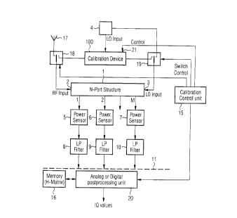
Fig. la shows a calibration device and a N-port structure designed for a on-
line
calibration,
Fig. lb shows a calibration device and a N-port structure according to the
present
invention designed for a off line calibration,
Fig. 2 shows a calibration device according to the present invention,
Fig. 3 shows the internal structure of the calibration device shown in Fig. 2
according to a first embodiment,
Fig. 4 shows the internal structure of a calibration device according to
another
embodiment,
1~
Fig. 5 shows the internal structure of a calibration device according to a
still other
embodiment,
Fig. 6 shows a N-port receiver based on a N-port junction with an active
circuitry
with isolation function, ,
Fig. 7 shows a mathematical representation of a N-port receiver,
Fig. 8 shows a functional description of a N-port receiver,
Figs. 9 to 14 show simulation results.
Figs. 15 and 16 show a six-port receiver with calibration devices according to
the prior
art, and
Figs. 17A, 17B and 18 show the general concept of N-port junction based
receivers.
Detailed Description of the Preferred Embodiments
CA 02310924 2000-06-07
9
The solutions according to the present invention allow a simple calibration of
N-port
receivers, which are commonly used as IQ demodulators or direct demodulators
of (n)
PSK (n) QAM oscillator modulation schemes. Thereby a local oscillator is used
as a RF
source. After processing of the input RF signal originating from the local
oscillator,
calibration signals are provided to at least one of the inputs of the N-port
receiver. This
presents a simple technological solution to generate the required calibration
signals only
from the already available LO/RF source via an easy to implant passive
circuitry. A
more complicated generation of the calibration sequences (modulation, etc.)
and an up-
conversion block are no longer necessary. This calibration technique may cope
with
various effects Iike non-ideal matching of the power sensing devices, non-
ideal
matching of the associated gain block (providing RF/LF isolation) in very
large passive
element tolerances.
With reference to Figure la an embodiment of the present invention will be
explained,
wherein said embodiment is designed for an off line calibration.
As shown in Figure la, the central elements are a calibration device 100 and a
N-port
structure 1. In the usual operation, a RF signal originating from an antenna
17 is input
to a first input 2 of the N-port structure 1. A local oscillator RF signal
originating from
a local oscillator 4 is input to the second input 3 of the N-port structure 1.
As it is
known from the prior art, the N-port structure (N being an integer larger than
two) has
N-2 terminals connected respectively to a power sensor 5, 6, 7 which supplies
output
signal respectively to a Iow filter 8, 9, 10. The filtered output signal of
the low pass
filter 8, 9, 10 is supplied to an interface 11 and than to an analog digital
post processing
block 17.
In case a calibration process is to be effected, a calibration control unit 15
controls
switches 18, 19 as the calibration device 100 such that the first RF input 2
and the
second (LO) input 3 of the N-port structure are supplied by output signals of
the
calibration device 100. The RF signal from the local oscillator 4 is supplied
to the
calibration device 100. The calibration device 100 processes the RF signal
from the
local oscillator 4 and supplies calibration signals to the first RF input 2
and the second
(LO) input 3 of the N-port structure 1, respectively.
CA 02310924 2000-06-07
The calibration control unit 15 furthermore controls the calibration device
100 at a
control terminal 18.
5 When a calibration process is effected and the corresponding calibration
signals are fed
from the calibration device 100 to the first and second input 2, 3 of the N-
port structure
1, the analog or digital post processing unit 17 detects the output signals of
the low pass
filter 8, 9, 10 and calculates calibration coefficients which are stored in a
memory 16.
The analog or digital post processing unit 17 is also controlled by the
calibration control
10 unit 15 to switch from normal operation to calibration and vice versa. In
the normal
operation the analog or digital post processing unit 17 outputs detected IQ-
values
calculated on the basis of the output signals of the low pass filter 8, 9, 10.
As can be seen from Figure la, the RF signal from the local oscillator 4 alone
is the
base for the calibration process and the calibration device 100 processes said
RF signal
from the local oscillator 4, such that a calibration sequence generator in the
baseband
regime with subsequent up-conversion to the operation frequency is no longer
necessary .
The interfaces necessary to connect the off-chip calibration devices are also
shown in
figure la.
Figure lb shows a modification of the scheme according to Figure la. According
to the
embodiment of Figure la the calibration process is controlled by an external
calibration
hardware 15 controlling a switch 18 and the calibration device 100.
Furthermore the
external calibration hardware is connected to the memory 16 to store
calculated
calibration coefficients. To said effect to the external calibration hardware
15 is
connected to the DC interface 11, such that the external calibration hardware
can
calculate the necessary calibration coefficients, which are subsequently
stored in the
memory 16.
Figure 2 shows a calibration device according to the present invention. The
calibration
device 100 is supplied with a RF signal from a local oscillator at an input
terminal 101.
CA 02310924 2000-06-07
lI
Furthermore a control terminal 21 is provided. The calibration device 100 has
two
output terminals, of which one is connected to the first RF input 2 of the N-
port
structure (output terminal 102) and the second output terminal (local
oscillator output
terminal I 03 ) .
Figure 3 shows a first embodiment for the internal structure of the
calibration device
100. The RF signal from the local oscillator 4 is supplied to the input 101 of
the
calibration device 100 and then to a power splitter 104. The power sputter 104
generates a first branch supplied without further processing (apart from
switching 106)
to the local oscillator output terminal 103. The other branch generated by the
power
splitter 104 is supplied to a switch 105 controlled a control signal supplied
to the
control input terminal 21 of the calibration device 100 depending on the
control of the
switch, this branch calibration signal is either directly supplied to another
switch 109
controlled by the control signal from the control terminal 21 (option a),
phase shifted
by a phase angle ø 1 of a phase shifter 107 (option b) or phaseshifted by a
phase angle
~ 2 by means of a phase shifter 108. In operation during the calibration
process the
switches 105 and 109 are controlled such that time sequentially the
calibration signal a,
the calibration signal b and the calibration signal c, i. e. calibration
signals with
different phase shifts relatively to each other are supplied to the switch 109
and thus to
the RF output terminal 102 of the calibration device 100.
Figure 4 shows a further embodiment of the internal structure of the
calibration device
100. In comparison to the embodiment in Figure 3, an attenuator 110 is
connected in
the signal pan of the calibration signal option a.
Figure 5 shows a further embodiment of the internal structure of the
calibration device
100. According to said embodiment also the signal branch supplied to the local
oscillator output terminal 103 is processed such that either the signal
without phase shift
(option c) or a calibration signal with a phase shift ~ 3 (option d) is
supplied to a switch
114. The switch 114 is connected to a ground by a termination I13. According
to said
embodiment another common feature to the option of Figure 2 and Figure 3,
potentially
CA 02310924 2000-06-07
12
four different calibration signals are supplied to the output terminal 102 and
103,
respectively.
Generally the calibration device 100 comprises at least one phase shifter, at
least one
switch and at least one power splitter.
The calibration device can be integrated together with the N-port structure 1.
The N-
port device, the power sensors and the calibration device can be manufactured
also as a
mufti-chip solution or a two-device solution.
As has already been explained with reference to Figure la, the calibration
procedure
using the calibration device according to the present invention can be
performed off-
line. The obtained calibration coefficients are stored in the memory and used
for the
operation of the N-port receiver as they are taken into account by the analog
or digital
post processing unit 20 in normal operation. Temperature caused RF drifts can
be
compensated off-line by a calibration procedure resulting in up-dated
coefficients.
In Figure 3 a calibration device is presented which consists of one power
splitter, three
switches and at least two phase shifters. A power splitter provides the LO
signals to left
and right branches. The signal in the left branch is further provided to
switch number 2.
With this switch one of the three paths is selected, where one of the paths
may have no
phase shifter and the remaining two paths have two different phase shifters.
These RF
and LO output signals are then provided to the first and second input of the N-
port
receiver, respectively.
In Fig. 4 a calibration device is presented which consists of one power
splitter, two
switches, at least two phase shifters and at least one attenuator. The power
splitter
provides the LO signals to the left and right branches. The signal in the left
branch is
further provided to switch number 2. With this switch one of three paths is
selected,
where one may have one attenuator and the remaining two paths have two
different
phase shifters. These RF and LO output signals are then provided to the first
and
second input of the N-port receiver, respectively.
CA 02310924 2000-06-07
I3
In Fig. 5 a calibration device is presented, which consists of one power
splitter, four
switches and at least two phase shifters. The power splitter provides the LO
signal to
the left and right branches. The signal in the left branch is further provided
to switch
number 2. This switch is able to select one of two paths, where one of the
paths may
have one phase shifter. The second path does not need to have any phase
shifter. A
similar topology is possible for the right branch. The difference is that
switch no. 3
may have three states where it may totally suppress the incoming LO signal.
These RF
and LO output signals are then provided to the first and second input of the N-
port
receiver, respectively.
All switches, phase shifters, and power sputters may be realized by a
plurality of the
technology.
Figure 6 shows preferred embodiment of the internal structure of the N-port
structure 1.
According to said embodiment the N-port structure is a five-port structure 1
comprising
a passive three-port structure 12 connected to a passive four-port structure
14 by means
of an active circuitry with RF isolation function (block 13). The passive
three-port
structure 12 is connected to a power sensor.5 which supplies an output signal
to a low
24 pass filter 8 which is connected to the DC interface 11. The passive four-
port structure
supplies two output signals power sensors 6, 7, which are respectively
connected with
the low pass filter 9, 10 supplying output signals to the DC interface 11.
Mathematical Background
Due to manufacturing tolerances, reflections from power sensors or active
devices, and
a great variety of possible implementations of the N-port structure, a general
calibration
is desirable, which accounts for the tolerances and imperfections.
Thus, first a general set-up and calibration procedure will be discussed,
before applying
it to a specific structure. The mathematics here applies to a 5-port device
with two
inputs and three power sensors. The 5-port device is only an example for N-
port
devices, N being an integer larger than two.
CA 02310924 2000-06-07
14
The measured powers P = (P, , Pz , P3 ~T are solely dependent on the structure
of the 5-
port, represented by a 3*4 matrix D and the IQ-values, assembled in
v=(I'aF~l'LQ~1~~)r via
P=DY
The IQ values are defined as 1= I s~ cos ~, Q = Is~.l sin ~ with a complex RF
signal sRF
and the phase difference ~ between RF and LO input. By adding the assumed LO
power
14 PLO as a forth component to the power vector and by introducing a forth row
(0 I 0 0)
in D , the above matrix equations gets invertible almost always. Then the IQ
values can
be reconstructed via
P
V = o Eq. 1
PLo
All 16 elements of the reconstruction matrix H can be calculated from four
independent measurements of known input values. This procedure will be called
the
calibration process. Mathematically it is expressed as
P PZ P3' Pro ~ P'aF. Pc,'o
I' Q'
- Pz Pz2 P3Z Pro P~ Pio 1 Z Qz
2o H =
J 3 3 3 3 3 3 Q3 Eq. 2
P' PZ P3 Pco PxF Pco I
P PZ P34 Pco P~ Pco I4
where the superscript denotes the number of the measurement.
For a well-suited and robust calibration in the presence of noise, it is
extremely
important to carefully select the calibration sequence. It has to be one that
leads to a
low condition number of both, the power matrix (left) and the IQ (right)
matrix. The
CA 02310924 2000-06-07
' 15
latter determines the calibration sequence and should be designed for
simplicity and
robustness.
Finally, the IQ values are calculated via
P,
m h3z h33 h3a p2 Eq. 3
h h h h P
at az a aa~
3 3
Pco
Thus, for reconstruction of the IQ values, only eight real multiplications are
required.
A method of operation is described using a 5-port receiver with RF/IF
isolation
functionality (shown in Fig. 6). It consists of a 3-port (RF input), an active
or non-
reciprocal circuitry providing an isolation function and possibly some
amplification of
the RF input signal. A phase shifter interconnects the additional two 3-ports.
The phase
shift should be unequal to m~/2 (m is an integer value), an advantageous value
would
be ~/4. An alternative topology for 5-port structure may be seen in Figure 8.
At all
three output ports the powers of the signals are measured and low pass
filtered. The
complex vector ratio between LO and RF signal can be reconstructed within a
DSP or
especially designed analogue circuitry.
Calibration Sequences and their generation
According to the described mathematical model, different sequences may be
used, but
the key features for their choice are:
~ they have to Iead to well conditioned matrices in order to obtain a robust
calibration
~ they have to be simple, in order to be realized by the simple RF treatment
of the LO
signal, with a minimum number of switches, phase shifters and attenuators.
The choices of simple and sufficiently stable calibration sequences are shown
in Tab. 1.
CA 02310924 2000-06-07
. ' 16
1 (equal power) 2 (equal LO signal)
No. SLR S~ S~Q SRF
1 1 1 1 lh
2 1 j 1 j
3 0 1 1 1
4 1 -(1+j)/~ 1
J
t ame t c:atlbratlon signals
Other signal sequences are also possible. However, the above are well suited
and very
simple to generate.
The signals can be created by a simple passive or active circuit entity,
examples of the
realization are shown in Fig. 3, 4, 5.
Generally, during the calibration process four different known complex signals
are sent
to the RF and LO input. For each signal pair, the power levels are measured
and
stored. After all signals have been applied and powers have been measured, the
device
matrix H is calculated according to Eq. 2.
For the above example the proposed calibration has a complexity of:
~ 4 different pairs of signals need to be applied,
~ 4 real IQ vectors (4 values) for the calibration signals need to be stored,
~ 4 real power vectors (4 values ) need to be stored,
~ one real 4 by 4 matrix needs to be inverted,
~ two 4 dimensional vectors need to be multiplied with one 4 by 4 matrices.
The calibration of the N-port device can be done at different stages of life-
cycle and
operation:
1. After manufacturing the N-port is calibrated via a highly accurate
calibration device
as described above, the extracted H-matrix is stored in the memory and further
used
for the calculation.
Advantages:
CA 02310924 2000-06-07
17
~ The N-port receiver device is accurately calibrated,
~ It needs to be calibrated only once, so that the calibration device itself
does not
need to be part of the total receiver circuitry,
~ Calibration is done off-line, thus, the final system does not require any
calibration
control logic,
~ Calculations of the H-matrix elements are done off-line. So the internal DSP
only
has to store 8 elements and the IQ values are calculated involving e. g. two
dot-
products with 4 dimensional vectors.
Disadvantages:
~ Aging, temperature drift cannot be accounted for.
2. The calibration is done on-line, e. g. during initialization or at some
time during
operation of the device.
Advantages
~ Errors due to aging and drift effects are accounted for
~ A one-chip solution is possible
~ Nothing needs to be done after manufacturing, every calibration is done
later and
automatically.
Disadvantages:
~ Due to tolerances even in the calibration device, the error correction is
less
accurate,
~ Some calibration logic is needed within the final device.
~ All computations have to be done on board. Thus the requirements for digital
processing are large.
However, repeating the calibration can significantly reduce the influence of
variations,
fluctuations, and noise during the calibration process. The computed power and
IQ
matrices are then averaged, so that a significantly more accurate error
correction
achieved.
After calibration, the H-matrix is calculated and the required eight elements
are stored.
During every measurement cycle three powers are detected. In a DSP or some
analog
circuitry the ppwer values including the initially known power of the local
oscillator are
CA 02310924 2000-06-07
~ 18
multiplied by the 2 by 4 elements of the correction matrix. Finally the IQ
values are
available at the output of the DSP.
The final calibration matrix may be recalculated by the following methods of
operation:
1. One sequence, consisting of four complex states, is sent to the N-port
receiver input
and all related 8 real calibration coefficients are calculated and stored into
the
memory for use in error correction.
2. One sequence that consists of four complex states is sent to the N-port
receiver inputs
several times. The related eight real calibration coefficients are calculated
after each
sequence. After all repetitions are done, the averages of alI the calibration
coefficients are calculated and stored in the memory for further use in error
correction.
3. Different sequences, consisting of four complex states, are sent to the N-
port
receiver input and the related 8 real calibration coefficients are calculated.
After all
sequences are sent, the coefficients are averaged and are stored in the memory
for
later use in error correction.
4. Combinations of items 2 and 3 (above) can be used.
5. A long calibration sequence, consisting of at least four complex states, is
sent to the
receiver input and the IQ-values and measured power values are stored in the
memory. The related 8 calibration sequences are calculated e. g. by means of
~ generalized inversion of the power matrix,
~ a least square algorithm,
~ any possible method to solve general rectangular systems of equation.
The coefficients are stored and used for later error correction.
In Table 2, calibration coefficients (four for I values and four for Q value)
are
calculated, using three different sets of sequences. It may be observed that
the
deviations of the coefficient are very small in all the cases, so that
averaging may be
performed in order to obtain the final values.
. CA 02310924 2000-06-07
19
Cal. sequence h;, h;2 h;3 h.4
(1) equal LO 4.7673 -2.5437 -1.7942 0.5385
(2) equal phase 4. 8164 -2.5517 -1. 83400.5348
I (3) condition (69) 4.7780 -2.5334 -1.8112 0.5347
(4) ideal cal. 4.7703 -2.5342 -1.7889 0.5381
( 1) equal LO -2.9099 2.2468 -1.7830 0.3760
Q (2) equal phase -2.8260 2.2287 -1.8498 0.3640
(3) condition (69) -2.9619 2.2467 -1.5823 0.3788
(4) ideal cal. -2.8622 2.2361 -1.7889 0.3703
Table 2: Calibration coefficients, originating from three different sets of
calibration
signals ( 1, 2) as in Tab. 1, (3) with a badly conditioned IQ-matrix, (4)
ideal
(undisturbed) calibration signals.
Accuracy enhanced error correction for N-port devices with isolation function
For further improvement of the calibration and operation of the receiver it
may be
desirable to isolate power sensor 1 (Fig. 1, 6) from the LO port. This can be
done by a
great variety of realizations e. g. non-reciprocal or active elements,
elaborated passive
(resistive)) circuit design.
In such a design, the first power (P,) is directly proportional to the power
of the 1ZF
signal. additionally, there are only few passive circuit elements in the
signal path and it
can be assumed that errors and tolerances are less critical.
With such a design, it is possible to get a very accurate estimate for the
power of the
incoming RF signal, which can be exploited to enhance the accuracy of the IQ
signals.
During calibration one additional factor Hp is calculated via the simple
operation
N
~ PRF
1 ,_
Equ. 4
P;
CA 02310924 2000-06-07
During operation, one additional value P',~ = P,lHP is calculated from the
detected
value P,. It can be assumed, that the new factor P'~. is more accurate than P~
calculated from Eq. 1 and thus should be used to enhance the accuracy of the
IQ-values
5 via
I'=I PRF . Q~=Q p~ , Equ.S
Iz +Q2 Iz +Qz
10 s~ RF signal to be I/Q demodulated
sLO Second RF signal (known, usually local oscillator)
Phase angle between RF and LO signal
Y, P (Vector) collection of IQ values and measured powers
Gain of the amplifier stage (complex)
15 i", i22 Complex input and output reflection coefficients of the
amplifier
I, Q, I', Q' In- and quadratur phase components of s~
P~. P2, P3 Detected powers at respective sensors
Pr~~ Pro RF and LO powers
X' i-th calibration signal X
20 D Transfer matrix of the device
H,hj Device matrix for calculation of IQ values, elements of
the matrix
'fable 3. Legend of used Variables
Verification of the proposed solution by simulations
As a numerical example the 5-port structure (related to Fig. 6) was under
investigation.
All 3-port structures are considered equal. Each of them is treated as star
connected
resistors, where each of them is having Z/3 resistance (Z is the
characteristic
CA 02310924 2000-06-07
' 21
impedance, usually 50 SZ). Each resistor has a parasitic reactive pan of Z/60.
The
active circuitry with isolation function is realized by a simple non-matched
amplifier
having 10 dB gain, and equal input and output reflection loss i, ~ =i" _ -6dB.
Results are
presented for 16 QAM signals, with and without associated noise. A
mannfa~r"r;n.,
tolerance of 20 % is assumed. During operation the variation of all circuit
elements is
1 % . The local oscillator has a 10 % variation even during calibration.
During this
phase, all tolerances are applied and all the calibration signals are assumed
to have a
tolerance of 1 % or 20 % , respectively. In Fig. 9 and 10 calibration sequence
( 1) of Tab.
1 is used and three different cases are compared, the RF-QAM signal is
noiseless.
Without calibration (~), the device will not allow a correct detection of the
symbols,
whereas in the calibrated case (+), the noise is significantly reduced and the
device will
allow a low bit error rate. The variation in this case originate solely from
element
variations during operation ( 1 % ) and LO noise ( 10 % ) . The constellation
can be further
improved by enhancing the accuracy via an N-port structure with isolation
function(0)
as described above. The same is true for the second calibration sequence. The
simulation results are shown in Fig. 11, 12.
In order to prove the functionality of the system in the case of larger drift
and element
value variation during operation, in Fig. 13 a simulation result is shown for
element
tolerances of 10 % for the best possible calibration scheme. This case may
occur, when
calibrating the N-port off line, e. g. directly after manufacturing. At last,
the effect of
noise in a worst case scenario is examined. Again, high tolerance of the
element values
of 10 % and a signal to noise ratio of 20 dB of the RF signal are assumed.
Fig. 14
proves that the calibration scheme does still work even under these
conditions.
A new calibration device and method of calibration for N-port receiver
structure of
digitally modulated signals, is proposed.
Proposed device and related method of operation offers a simple implementation
solution, with minimum additional RF circuitry, where available LO signal is
reused.
The main advantage of the proposed technology is that calibration sequences
are
generated only by the usage of the LO signal and additional passive RF
circuitry of the
. CA 02310924 2000-06-07
' 22
calibration device. Output signals of the calibration device are connected to
the N-port
receiver in order to perform the proposed calibration. Therefore there is no
need to
have an additional RF source, which has to be modulated.