Note: Descriptions are shown in the official language in which they were submitted.
CA 02311444 2000-OS-25
WO 99/27807 PCT/EP98/07556
- 1 -
DESCRIPTION
ELECTROMAGNETIC FIELD DEFLECTING GARMENT
The present invention concerns a garment capable of deflecting electromagnetic
fields
arising from outside sources.
At present there are no examples in the clothing field of garments that
deflect
electromagnetic fields.
The need to produce this type of garment has arisen recently precisely because
the
quantity of electromagnetic waves to which the human body is exposed has risen
considerably.
l0
In the home environment we are continually bombarded by electromagnetic fields
originating from radio transmitters and receivers that propagate waves in the
radiofrequency range, from liquid crystal displays of various items of
electronic
equipment and above all phosphorus screens of televisions that transmit
electromagnetic
waves at a frequency concentrated around 900 GHz.
In the working environment we are often obliged to stay constantly in front of
the
monitor of a computer which, like a television set, transmits electromagnetic
waves at a
frequency around 900 GHz.
Outdoors it often happens that we pass near high voltage power cables and
these too give
off electromagnetic waves. Furthermore, there has recently been a strong
development of
the GSM cellular telephone network resulting in a considerable spread in the
use of
cellular telephones and these also emit electromagnetic waves around a
frequency of 1 S
2 5 GHz.
Recent medical studies have ascertained that any charge of an electrical or
electromagnetic nature that is absorbed the human body impairs the cellular
balance of
the chondrioma. The chondrioma is a cellular structure formed by the
chondriosomes
3 0 which are cytoplasmic bodies in the form of granules, filaments and rods
thought to be
responsible for a major part of cell physiology.
CA 02311444 2000-OS-25
WO 99127807 PCT/EP98/07556
- 2 -
The human body initially reacts by compensating for the cellular imbalances in
the
chondrioma caused by electromagnetic radiation, but in the long term these
imbalances
are no longer compensated and this causes poor cell physiology with consequent
harmful
effects on human health.
The object of the invention is to prevent such problems, providing a garment
that is
simple to make.
This object is achieved according to the invention, with the characteristics
listed in the
appended independent claim 1.
Preferred embodiments of the invention appear from the dependent claims.
The garment according to the invention is made by means of a lattice-pattern
conductive
fabric connected to an electronic circuit. Said conductive fabric absorbs the
electromagnetic fields and directs them towards the electronic circuit where
they are
dissipated through the Joule effect. The garment can act as a sort of Faraday
cage
discharging the electromagnetic signal to ground. The ground must obviously be
understood as a virtual ground, since grounding of the circuit is achieved by
means.of a
2 o connection thereof to a cord of conductive material, acting as a ground
plate.
Any parallel resonator characterized by a -high cutting frequency so as to act
as a low-
pass filter and cut off all the signals at a frequency above said cutting
frequency can be
used as the electronic circuit.
It is possible to connect a micro-amperometer to the circuit capable of
providing a
measurement of the electromagnetic field present in whatever point the user
happens to
be. The user thus knows when his garment is absorbing and deflecting an
electromagnetic
field and knows the magnitude of said field.
Said garment is particularly useful for users who spend long periods in front
of a
television screen or who for reasons of work are subjected to the radiation of
a computer
monitor.
CA 02311444 2000-OS-25
WO 99/27807 PCT/EP98/07556
- 3 -
r
Furthermore the garment according to the invention can have a pocket
especially for
holding a cellular telephone so as to protect the user from the magnetic
fields given off
by said telephones.
Further characteristics of the invention will be made clearer by the detailed
description
that follows, referring to a purely exemplary and therefore non-limiting
embodiment
thereof, illustrated in the appended drawings, in which:
Figure 1 shows a plan view of a jacket according to the invention;
Figure 2 shows a plan view of the jacket in Figure 1 open;
Figure 3 shows a plan view of a detail of a fabric of the jacket in Figure l;
Figure 4 shows a plan view of a detail of the edging weave of the jacket in
Figure 1;
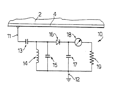
Figure 5 shows the electrical diagram of an electronic circuit according to
the invention;
Figure 6 shows a phase diagram and a diagram of the voltage gain according
to.the
2 0 frequency of the electronic circuit in Figure 5;
Figure 7 shows an axonometric view of a further embodiment of the invention.
The garment according to the invention is described with the aid of the
figures.
Reference is made purely by way of example to a magnetic field deflecting
jacket 1,
consisting of dry, conductive knitted fabric 2. Filaments 3 of conductive
material which
can preferably be tungsten and carbon are woven parallel into the weave of
said fabric ~.
Said filaments 2 are able to conduct the electromagnetic fields that gather on
the jacket 1.
The jacket 1 is edged around the perimeter with a crisscrossed lattice fabric
4. The fabric
4 has crisscrossed lattice filaments 5. The filaments 5 must be made of
conductive
material, preferably tungsten and carbon. The crisscrossed lattice fabric 4 is
disposed on
the edge of the jacket l and is folded over, being made of a thicker and
closer weave than
3 5 fabric 2 and serves to close the conductive circuit that has been created
in the jacket 1.
CA 02311444 2000-OS-25
WO 99/27807 PCT/EP98/0'7556
-
The jacket 1 can also be covered with a non-conductive material at said
edging; purely by
way of example velvet can be used as the covering material for the edging. The
jacket 1
can be made in a single block or can have closing means such as buttons 6 or
zips.
A pocket 7 made of conductive fabric can be made on the inside or on the
outside of the
jacket 1. Said pocket 7 can preferably be of such a size as to contain a
mobile telephone 8
according to the shapes and size most commonly used commercially or any other
object
of a similar size.
An electronic circuit 10 is positioned in a special housing 9 that can be made
inside the
jacket 1 so that the circuit 10 is hidden. The circuit 10 is connected by
means of a
conductor wire 11 to the edging fabric 5 of the jacket 1. Grounding of the
circuit is
obtained by means of a cord 12 made of conducting material, preferably copper.
The cord
12 is made to hang from the jacket 1, so as to be able to discharge the
electromagnetic
field present on the jacket 1.
The electronic circuit 10 can be any parallel resonator circuit with a
specific cutting
frequency and resonance frequency. Said circuit 10 must be able to disperse
the
electromagnetic signal coming from the jacket 1 through a Joule effect and
must be able
2 0 to cut off the signals above its cutting frequency.
Figure 5 shows a possible embodiment of the electrical diagram of the circuit
10. A
coupling capacitance 13 is positioned between the edging fabric 4 and the
parallel
resonator circuit. The parallel resonator consists of the connection in
parallel of an
inductance 14, two capacitances 15, 17 and a resistance 19. The two
capacitances 15 and
17 are decoupled by means of a diode 16 for stabilization of the supply to the
circuit 10.
A micro-amperometer 18 is connected between the capacitance 17 and the
resistance 19.
Said micro-amperaometer 18, more or less the size of a wrist watch, can be
digital or
3 0 analogic and is positioned in a special housing 21 made in the outer part
of the jacket so
as to be visible to the user, and is connected to the electronic circuit 10 by
means of
connecting cables 20. The user can thus read the intensity of the
electromagnetic field
absorbed by the jacket 1 at any time.
3 5 The resistance 19 must preferably be chosen with a very high value, about
2 MSZ, in
order to be able to disperse the electromagnetic signal coming from the jacket
through a
CA 02311444 2000-OS-25
WO 99/27807 PCT/EP98/07556
- 5 -
Joule effect. The power dispersed by said resistance 19 is in the order of
nano Joules.
This leads to a minimal increase in temperature, quantifiable as about half a
degree
centigrade.
The coupling capacitance 13 can be chosen with a value of about 100 pF. The
capacitances 1 S, 17 of the resonator can be chosen respectively with a value
of 20 pF and
~1.F, so that their parallel gives a capacitance of about 20 pF. For the
stabilizing diode
16 a commercially available model 1N32A can be used. The inductance 14 of the
parallel
resonator can be chosen with a value of 101..~,H.
In Figure 6 a phase diagram of the circuit according to the frequency and a
diagram of the
voltage gain according to the frequency are shown. Said diagrams are obtained
as the
output taken on the resistance 19 when a sinusoidal signal with a frequency of
1 kHz is
given as the input to the circuit. From the phase diagram two changes of phase
can be
noted, with a phase shift of 90° around 10 Hz and a phase shift of
180° around 7 MHz.
From the voltage gain diagram we see a peak around 7 MHz, the frequency that
corresponds to the cutting frequency of the circuit. Below this cutting
frequency of the
circuit the signals coming from the jacket 1 are filtered.
Figure 7 shows a further embodiment of the invention represented by a hat made
of the
knitted conducting fabric 2 and an edging made of the conducting lattice
fabric 4. The
electronic circuit 10 connected by means of the conducting wire 11 to the
edging of the
hat is positioned inside said hat. A cord 12 hangs from said circuit and acts
as the ground.
This embodiment is particularly effective in the case of use of cellular
telephones. In fact
by wearing the hat according to the invention while communicating with the
cellular
telephone near the ear, the electromagnetic fields coming from the phone are
deflected: -'