Note: Descriptions are shown in the official language in which they were submitted.
CA 02311470 2000-OS-19
WO 99/27732 PGT/GB98/03416
CALIBRATION OF A SUBSCRIBER TER1VIINAL FOR A WIRELESS
TELECOVII~iUNICATIONS SYSTEM
FIELD OF THE INVENTION
The present invention relates generally to subscriber terminals for wireless
telecommunications systems, and more particularly to techniques for
calibrating such
subscriber terminals.
BACKGROUND OF THE INVENTION
A wireless telecommunications system has been proposed in which a
geographical area is divided into cells, each cell having one or more central
terminals
(CTs) for communicating over wireless links with a number of subscriber
terminals
(STs) in the cell. These wireless links are established over predetermined
frequency
channels, a frequency channel typically consisting of one frequency for uplink
signals
from a subscriber terminal to the central terminal, and another frequency for
downlink
signals from the central terminal to the subscriber terminal.
The system finds a wide variety of possible applications, for example in
rural,
remote, or sparsely populated areas where the cost of laying permanent wire or
optical
networks would be too expensive, in heavily built-up areas where conventional
wired
systems are at full capacity or the cost of laying such systems would involve
too much
interruption to the existing infrastructure or be too expensive, and so on.
In one embodiment, the central terminal may be connected to a telephone
network and exists to relay messages from subscriber terminals in the cell
controlled
by the central terminal to the telephone network, and vice versa. By this
approach,
an item of telecommunications equipment connected to a subscriber terminal may
make an outdoing call to the telephone network, and may receive incoming calls
from
the telephone network.
However, such a wireless telecommunications system is not restricted to use
with telephone signals, but could instead handle any other appropriate type of
telecommunications signal, such as video signals, or data signals such as
those used
for transmitting data over the Internet, and in order to support new
technologies such
as broadband and video-on-demand technologies.
CA 02311470 2000-OS-19
WO 99/27732 PCT/GB98/03416
Figure 1 illustrates an example of a typical prior art configuration for a
subscriber terminal for such a wireless telecommunications system. Figure I
includes
a schematic representation of customer premises 22. A customer radio unit
(CRU) 24
would typically be mounted on the customer's premises and may include a flat
panel
S antenna or the like 23. The customer radio unit is mounted at a location on
the
customer's premises, or on a mast, etc, and in an orientation such that the
flat panel
antenna 23 within the customer radio unit 24 faces in the direction 26 of the
central
terminal for the service area in which the customer radio unit 24 is located.
The customer radio unit 24 is typically connected via a drop line 28 to a
power
supply unit (PSU) 30 within the customer's premises. The power supply unit 30
is
connected to the local power supply for providing power to the customer radio
unit
24 and to a network terminal unit (NTU) 32. The customer radio unit is also
connected via the power supply unit 30 to the network terminal unit 32, which
in turn
is connected to telecommunications equipment in the customer's premises, for
example
to one or more telephones 34, facsimile machines 36 and computers 38. The
telecommunications equipment is represented as being within a single
customer's
premises. However, this need not be the case, as the subscriber terminal 20
may
support more than one line, so that a number of items of subscriber
telecommunications equipment could be supported by a single subscriber
terminal 20.
The subscriber terminal 20 can also be arranged to support analog and digital
communications, for example analog communications at 16, 32 or 64Kbits/sec or
digital communications in accordance with the ISDN BRA standard.
The CRU 24 typically includes all of the necessary processing circuitry to
convert incoming wireless telecommunications signals into signals recognisable
by the
items of telecommunications equipment, and also to convert such signals from
those
items of telecommunications equipment into wireless telecommunications signals
for
transmission from the antenna 23.
A significant problem with this approach is that the CRU 24 is an expensive
item of equipment to replace. Since this is generally located on the outside
of the
customer's premises, it is prone to theft. In addition, all of the components
within the
CRU 24 have to be able to withstand the exposure to varying climatic
conditions that
, . . . . ( y
' f n f I C .
f s v . t I f n
P/3809.W0 , ' '' ' ; ~ ' ~ : ~ ~ : ; ; .
'f ,
,f, , " ", " I.
3
arise as a result of the CRU 24 being mounted externally. For example, the
components must be able to withstand significant variations in temperature,
and
variations in humidity.
However, one reason why the CRU 24 has previously included all of the
necessary processing circuitry to convert incoming wireless telecommunications
signals into signals recognisable by the items of telecommunications equipment
is that
it reduces the technical complexity of the subscriber terminal to have all of
the
processing circuitry in one housing.
Further, problems with attenuation of the wireless signals transmitted between
the central terminal and the subscriber terminal, and vice versa, have
previously
dictated that the processing circuits of the subscriber terminal should be
located
physically close to the antenna 23. To illustrate this, it will be appreciated
that a
signal transmitted from the central terminal at a predetermined power level
will be
attenuated as it is propagated to the antenna 23 of the subscriber terminal
20. Once
the signal has been received by the anterma 23, there will also be further
attenuation
within the subscriber terminal as the signal is passed from the antenna to the
processing circuits within the subscriber terminal. Clearly, the further away
those
processing circuits are from the antenna, then the greater the attenuation is
likely to
be. A signal strength threshold will be determined below which a signal cannot
be
processed by the processing circuits within the subscriber terminal 20. Hence,
in
order to improve the range of the wireless telecommunications system, it has
been
considered advisable to minimise the distance between the antenna 23 and the
processing circuitry of the subscriber terminal provided to process that
received
signal.
The above requirements have led to the development of subscriber terminals
such as those illustrated in Figure l, in which an expensive customer radio
unit 24
engineered to withstand exposure to varying climatic conditions has been
mounted on
the exterior of a subscriber's premises.
To alleviate this problem, International Patent Application No.
PCT/GB98/03420 filed by the applicant for the present application on the same
day
as the present application proposes providing a subscriber terminal comprising
two
-1~ ~,0
CA 02311470 2000-OS-19 Q
~ v n 1 I ( : f I 1 1
I 1 t i 1
r 1 ( ~ I ( I 1
P/3809.W0 ; ~ ' . ' . . , v 1 : v '
I, ,a, " ,"
3a
distinct signal processing units, the first signal processing unit being
associated with
an antenna of the subscriber
NOEO SNE~
CA 02311470 2000-OS-19
CA 02311470 2000-OS-19
WO 99/Z7732 PCT/GB98/03416
4
terminal, and the second signal processing unit being associated with an item
of
telecommunications equipment connected to the subscriber terminal. Signals are
transmitted from the antenna, and received by the antenna, via a wireless link
at first
frequencies within an operating frequency band. The first signal processing
unit
comprises a frequency converter for converting signals between said first
frequencies
and a second frequency. Typically, the second frequency will be less than the
first
frequency.
The first and second signal processing units are connected via a connection
medium, and the telecommunications signals are then passed between the first
and
second signal processing units via the connection medium at the second
frequency.
Given this approach, the second signal processing unit can then be formed from
signal processing circuitry which is independent of the operating frequency
band.
Hence, the same second signal processing unit can be used irrespective of the
operating frequency band used for the wireless communications between the
subscriber
terminal and a central terminal. Further, the above approach significantly
reduces the
amounts of circuitry required within the first signal processing unit
associated with the
antenna, thereby reducing the complexity of the first signal processing unit.
The actual location of the first and second signal processing units within the
subscriber's premises is a matter of installation choice. However, since the
first signal
processing unit is associated with the antenna, it is likely to be mounted
close to the
antenna, and so is likely to be mounted externally. In such an embodiment,
this novel
subscriber terminal arrangement offers significant advantages over the prior
art, since
the first signal processing unit contains significantly less processing
circuitry than the
customer radio unit of the prior art subscriber terminal. Assuming the first
signal
processing unit is manufactured to withstand external use, then the components
within
the first signal processing unit will have to be able to withstand the
exposure to
varying climatic conditions in the same way that the components within the
customer
radio unit of the prior art subscriber terminal had to withstand those
climatic
conditions. However, since the first signal processing unit has significantly
less
components, it is cheaper to produce a first signal processing unit with the
necessary
specifications than it is to produce a customer radio unit of the prior art.
~ ~ ~ ~ f r ( ( 1 1 1 n
1 1 r 1 l 1 r 1 1 r 1 t . 1
( . 1
r' , ;
P/3809. WO ; ' ~ ; , ,
1 " " , ,1 ;1,
Given that the first signal processing unit is cheaper than the customer radio
unit of the prior art, then it is also less prone to theft than the customer
radio unit of
the prior art subscriber terminal.
Whilst the above described novel subscriber terminal arrangement alleviates
5 the earlier described problems with prior art subscriber terminals, there
are still some
concerns that need to be addressed. One problem is how to compensate for
losses to
received and transmitted signals resulting from the passing of those signals
over the
connection medium. It is desirable to compensate for these losses so as to
limit the
dynamic range of the signal as received at the far end of the connection
medium,
since limiting the dynamic range of the signal simplifies the circuit design.
Further,
without some form of compensation, accurate measurements of parameters of the
signals (eg. received or transmit signal level) cannot be made after the
signals have
been passed over the connection medium.
However, when providing circuitry to determine the necessary compensation,
it is desirable to keep to a minimum the circuitry within the first signal
processing
unit, since otherwise the provision of such circuitry would conflict with the
general
aim of trying to reduce the amount of circuitry in the first signal processing
unit.
In EP0750405 a cable loss equalisation system for a wireless communication
equipment is disclosed. In this document RF cable loss is compensated by
measurement of DC resistance. The DC resistance is calculated by measuring the
DC
current in the cable and the difference in voltage at both ends of the cable.
From
these measurements the voltage difference can be calculated and then the DC
resistance. From the DC resistance the RF loss can be estimated.
The applicant has appreciated that this system can be improved upon. The
system of the present invention has the advantage that it measures actual RF
power
loss rather than meaning the DC current and voltages at either end of the the
cable
in order to estimate the RF loss.
SUMMARY OF THE INVENTION .
Viewed from a first aspect, the present invention provides a subscriber
terminal for communicating over a wireless link with a central terminal of a
wireless
telecommunications system, the subscriber terminal comprising: a first signal
CA 02311470 2000-OS-19
P/3809.W0 . ; ,;.. ; ,.; ,;. ,"
6
processing unit associated with an antenna to transmit and receive signals
over the
wireless link; a second signal processing unit remote from the first signal
processing
unit and associated with an item of telecommunications equipment to pass
signals
between said item of telecommunications equipment and the first signal
processing
unit; a connection medium connecting said first and second signal processing
units;
calibration logic within said second signal processing unit for providing on
the
connection medium control signals used to control circuitry in the first
signal
processing unit and to cause an RF signal having a predetermined power level
to be
passed on the connection medium between the first signal processing unit and
the
second signal processing unit to enable the calibration logic to determine the
RF
power loss introduced by the connection medium; compensation circuitry driven
by
the calibration logic to compensate for the RF power loss determined by the
calibration logic.
In accordance with the present invention, the subscriber terminal comprises
two distinct signal processing units, the first signal processing unit being
associated
with an antenna of the subscriber terminal, and the second signal processing
unit
being associated with an item of telecommunications equipment connected to the
subscriber terminal. First and second signal processing units are connected
via a
connection medium, and the telecommunications signals are then passed between
the
first and second signal processing units via the connection medium. As
described
earlier, this arrangement provides a number of advantages over the prior art
arrangement of subscriber terminals.
Further, in accordance with the present invention, calibration logic is
provided
within the second signal processing unit to provide on the connection medium
control
signals used to control circuitry in the first signal processing unit and to
cause signals
to be passed on the connection medium between the first signal processing unit
and
the second signal processing unit to enable the calibration logic to determine
the
signal power loss introduced by the connection medium. Compensation circuitry
is
then provided which is driven by the calibration logic to compensate for the
signal
loss determined by the calibration logic.
Hence, in accordance with the present invention, the connection medium is not
~~S
CA 02311470 2000-OS-19
. . . . . ( ( . n
' Pi38o9.wo ; ' ; ~ : ; , ; ' ; ,
only used for passing received signals from the first to the second signal
processing
unit, and transmit signals from the second signal processing unit to the first
signal
processing unit, but is also used to carry various signals used to calibrate
the
subscriber terminal to compensate for power losses to signals resulting from
the
passing of those signals over the connection medium.
By the above approach, the amount of circuitry required within the first
signal
processing unit associated with the antenna is reduced, thereby reducing the
complexity of the first signal processing unit, whilst still allowing for
determination
of the compensation required to compensate for power losses to received and
transmitted signals resulting from the passing of those signals over the
connection
medium.
In preferred embodiments, the compensation circuitry is provided within the
second signal processing unit, this further reducing the circuitry required
within the
first signal processing unit.
The signal power loss introduced by the connection medium may differ
depending on whether the signal is a signal received by the subscriber
terminal or a
signal to be transmitted by the subscriber terminal.
Hence, in preferred embodiments, the calibration logic is arranged to provide
a first control signal on the connection medium to cause a first test signal
having a
predetermined power level to be output on the connection medium by the first
signal
processing unit, the calibration logic being arranged to determine from the
first test
signal as received by the second signal processing unit the power loss to a
received
signal introduced by the connection medium.
Preferably, the compensation circuitry comprises a first variable attenuator
which is arranged to be settable by the calibration logic to compensate for
the
determined signal power loss to a received signal.
Further, in preferred embodiments, the calibration logic is arranged to cause
a second test signal to be output by the second signal processing unit on the
connection medium, and to issue a second control signal on the connection
medium
to cause the first signal processing unit to prevent the second test signal
being output
from the antenna.
AMEt~l~c0 SHEEN
CA 02311470 2000-OS-19
. , . . . . . , .~ ~ .
' ; ; . . . ~ ~ ; ;
Pl3809.W0 ~ ~ . , . . .
8
Preferably, the first signal processing unit is then arranged to determine an
indication of the signal strength of the second test signal at the first
signal processing
unit, and to output that indication on the connection medium to the second
signal
processing unit for use by the calibration logic to determine the signal loss
to a
transmitted signal introduced by the connection medium.
Further, the compensation circuitry preferably comprises a second variable
attenuator which is arranged to be settable by the calibration logic to
compensate for
the determined signal loss to a transmitted signal.
In preferred embodiments, the first signal processing unit comprises a first
serial communications controller for receiving the control signals from the
second
signal processing unit.
Further, a second serial communications controller is preferably provided in
said second signal processing unit, and is arranged to communicate with said
first
serial communications controller over said connection medium, the calibration
logic
being arranged to output a signal to the second serial communications
controller to
cause the second serial communications controller to pass the control signals
over the
connection medium to the first serial communications controller in the first
signal
processing unit.
This approach enables a serial communications link to be established over the
connection medium to enable the necessary control signals to be passed from
the
second signal processing unit to the first signal processing unit.
A number of benefits arise from calibrating the subscriber terminal to
compensate for the power losses introduced by the connection medium. Once this
has
been performed, the parameters of received and transmitted signals can be
accurately
determined even after the signals have passed over the connection medium.
One example of a situation where this calibration can be of benefit is during
installation of the subscriber terminal, where an engineer needs to align the
antenna.
In preferred embodiments, for the purposes of antenna alignment, the second
signal
processing unit comprises: signal strength determination logic for determining
the
signal strength of a signal received by the first signal processing unit via
the antenna,
and passed to the second signal processing unit via the connection medium, the
signal
CA 02311470 2000-OS-19 ~E~yfl~p SHED
... , ... ,~ ..
Pi3so9.wo : ' : . . . ' ' ; ' . . ~ . , . ' - .
8a
strength determination logic being arranged to provide on the connection
medium an
indication signal representative of the received signal strength; whereby an
indicator
located or locatable at or in proximity to the antenna may be driven in
response to the
indication signal provided on the connection medium to provide an indication
of the
received signal strength.
This has the advantage that it enables a single installation engineer to align
the
antenna whilst being provided with some indication of the received signal
strength,
even though the first signal processing unit associated with the antenna
includes no
circuitry for, determining the received signal strength, and for driving the
indicator.
Further, since the subscriber terminal has been calibrated to compensate for
the losses
introduced by the connection medium, the indication signal output over the
connection
medium for controlling the indicator may provide a calibrated value for the
received
ENOyO S,~EE~
CA 02311470 2000-OS-19
CA 02311470 2000-OS-19
WO 99/27'32 PCT/GB98/03416
9
signal strength.
The actual indicator device used to provide the indication of received signal
strength is a matter of design choice. In one embodiment, the first signal
processing
unit includes the indicator. However, alternatively, or in addition, an
indicator may
S be attached to an output port of the first signal processing unit.
The first signal processing unit may be physically separate from the antenna,
this providing for a greater flexibility over the choice of antenna. In such
situations,
to obtain the most benefit from the present invention, it is advisable for the
indicator,
whether part of the first signal processing unit, or attached to an output
port of the
first signal processing unit, to be positioned so as to be observable by the
engineer
whilst aligning the antenna. Typically, this will not be an issue, since the
first signal
processing unit is likely to be located close to the antenna unit. Indeed, in
alternative
embodiments, the first signal processing unit and the antenna may be
integrated into
a single housing.
The indicator may be arranged to provide any suitable output, either visual or
audible, for use by the installation engineer. However, in preferred
embodiments, said
indicator comprises a plurality of LEDs for providing the indication of the
received
signal strength.
In alternative embodiments, the indicator need not be connected to, or
included
within, the first signal processing unit, and can instead be connectable
directly to the
connection medium.
In preferred embodiments, said signal strength determination logic comprises
a demodulator to determine the received signal strength, and a processor for
generating
the indication signal output over the connection medium for controlling the
indicator.
The connection medium connecting the first and second signal processing units
may be any suitable connection medium for sending telecommunication signals
between the first and second signal processing units. However, in preferred
embodiments, the connection medium is a coaxial cable. The attenuation of a
signal
transmitted over a coaxial cable increases with the frequency of the signal.
This can
be compensated to some extent by appropriate amplification of the signal prior
to its
transmission over the coaxial cable. At the radio frequencies used for
communications
CA 02311470 2000-OS-19
WO 99/27732 PCT/GB98/03416
over the wireless link between the central terminal and the subscriber
terminal, which
are of the order of Gigahertz, the coaxial cable has been found to attenuate
the signal
to an unacceptable level. However, by appropriate choice of an intermediate
frequency lower than the frequencies used over the wireless link, it has been
found
5 that a coaxial cable does provide a suitable medium for transmitting signals
between
the first and second signal processing units. This is a significant advantage,
since
coaxial cable is relatively cheap, and hence the use of coaxial cable to pass
signals
between the first and second signal processing units helps to reduce the
overall cost
of the subscriber terminal. A further advantage of coaxial cable is that it is
also easy
10 to terminate.
Viewed from a second aspect, the present invention provides a second signal
processing unit for a subscriber terminal in accordance with the first aspect
of the
present invention, the second signal processing unit comprising calibration
logic for
providing on the connection medium control signals used to control circuitry
in the
first signal processing unit to cause signals to be passed on the connection
medium
from the first signal processing unit to the second signal processing unit to
enable the
calibration logic to detenmine a signal loss introduced by the connection
medium.
Viewed from a third aspect, the present invention provides a method of
calibrating a subscriber terminal arranged to communicate over a wireless link
with
a central terminal of a wireless telecommunications system, the subscriber
terminal
comprising a f rst signal processing unit associated with an antenna to
transmit and
receive signals over the wireless link, a second signal processing unit remote
from the
first signal processing unit and associated with an item of telecommunications
equipment to pass signals between said item of telecommunications equipment
and the
first signal processing unit, and a connection medium connecting said first
and second
signal processing units, the method comprising the steps of: (a) providing on
the
connection medium control signals generated by the second signal processing
unit; (b)
controlling circuitry in the first signal processing unit dependent on said
control signals
to cause signals to be passed on the connection medium from the first signal
processing unit to the second signal processing unit; (c) using the signals
generated at
said step (b) to determine within said second signal processing unit a signal
loss
CA 02311470 2000-OS-19
WO 99/27732 PCT/GB98/03416
11
introduced by the connection medium; (d) in response to the determination at
said step
(c), controlling compensation circuitry to compensate for the signal loss.
BRIEF DESCRIPTION OF THE DRAWINGS
The present invention will be described further, by way of example only, with
reference to a preferred embodiment thereof as illustrated in the accompanying
drawings, in which:
Figure 1 is a schematic illustration of an example of a typical prior art
subscriber terminal;
Figure 2 is a schematic overview of an example of a wireless
telecommunications system in which the present invention may be employed;
Figure 3 is an illustration of an example of a frequency plan for the
telecommunications system of Figure 2;
Figure 4 is a schematic block diagram of a subscriber terminal in accordance
with preferred embodiments of the present invention;
Figure 5 is a circuit diagram illustrating components within the RF block of
the subscriber terminal of preferred embodiments;
Figure 6 is a block diagram illustrating the main components of the customer
modem unit of the subscriber terminal of preferred embodiments;
Figure 7A is a circuit diagram illustrating the components within the radio
modem card used to perform IF processing in accordance with preferred
embodiments
of the present invention;
Figure 7B is a block diagram illustrating the main components of the CDMA
modem within the radio modem card which is used to control the circuitry of
Figure
7A;
Figures 8A and 8B provide more detailed illustrations of portions of the
circuitry illustrated in Figure 7;
Figure 9 is a diagram illustrating the spectrum utilisation of the drop cable
used
in subscriber terminals of preferred embodiments of the present invention;
Figure 10 provides a more detailed illustration of the serial communications
controller illustrated in Figure 7; and
Figure 11 illustrates the use of a receive signal strength meter that may be
used
CA 02311470 2000-OS-19
WO 99/27732 PCT/GB98/03416
12
in embodiments of the present invention to assist in antenna alignment during
installation of the subscriber terniinal.
DESCRIPTION OF PREFERRED EMBODIMENT
The present invention may be used in connection with any appropriate type of
telecommunications signal, for example a telephone signal, a video signal, or
data
signals such as those used for transmitting data over the Internet, and in
order to
support new technologies such as broadband and video-on-demand technologies.
However, for the purpose of describing a preferred embodiment of the present
invention, a wireless telecommunications system will be considered that is
used for
handling telephony signals, such as POTS (Plain Old Telephony Service)
signals.
For the purpose of describing the subscriber terminal of preferred embodiments
of the present invention, a wireless telecommunications system will be
discussed in
which a central station is connected to the public telephone network and
exists to relay
messages from subscribers in the cell controlled by the central station to the
public
telephone network, and vice versa. Figure 2 is a schematic overview of an
example
of such a wireless telecommunications system. The telecommunications system
includes one or more service areas 12, 14 and 16, each of which is served by a
respective central terminal (CT) 10 which establishes a radio link with
subscriber
terminals (ST) 20 within the area concerned. The area which is covered by a
central
terminal 10 can vary. For example, in a rural area with a low density of
subscribers,
a service area 12 could cover an area with a radius of 15-20Km. A service area
14
in an urban environment where there is a high density of subscriber terminals
20 might
only cover an area with a radius of the order of 100m. In a suburban area with
an
intermediate density of subscriber terminals, a service area 16 might cover an
area
with a radius of the order of lKm. It will be appreciated that the area
covered by a
particular central terminal 10 can be chosen to suit the local requirements of
expected
or actual subscriber density, local geographic considerations, etc, and is not
limited to
the examples illustrated in Figure 2. Moreover, the coverage need not be, and
typically will not be circular in extent due to antenna design considerations,
geographical factors, buildings and so on, which will affect the distribution
of
transmitted signals.
CA 02311470 2000-OS-19
WO 99127732 PCT/GB98/03416
13
The central terminals 10 for respective service areas 12, 14, 16 can be
connected to each other by means of links 13, 15 and 17 which interface, for
example,
with a public switched telephone network (PSTN) 18. The links can include
conventional telecommunications technology using copper wires, optical fibres,
satellites, microwaves, etc.
The wireless telecommunications system of Figure 2 is based on providing
fixed radio links between subscriber terminals 20 at fixed locations within a
service
area (e.g., 12, 14, 16) and the central terminal 10 for that service area. In
one
embodiment, each subscriber terminal 20 is provided with a permanent fixed
access
link to its central terminal 10. However, in alternative embodiments, demand-
based
access could be provided, so that the number of subscribers which can be
serviced
exceeds the number of telecommunications links which can currently be active.
The wireless telecommunications between a central terminal 10 and the
subscriber terminals 20 could operate on various frequencies. Figure 3
illustrates one
possible example of the frequencies which could be used. In the present
example, the
wireless telecommunications system is intended to operate. in the 3.4-3.6GHz
Band.
In particular the present example is intended to operate in the Band defined
by the
CEPT SE 19 Recommendation. Figure 3 illustrates the frequencies used for the
uplink
from the subscriber terminals 20 to the central terminal 10 and for the
downlink from
the central terminal 10 to the subscriber terminals 20 in preferred
embodiments. It
will be noted that 12 uplink and 12 downlink radio channels of 3.SMHz each are
provided about a frequency of 3502MHz. The spacing between the receive and
transmit channels is 100MHz.
Hence, a frequency channel will be defined by one uplink frequency plus the
corresponding downlink frequency. Techniques such as 'Code Division
Multiplexed
Access' (CDMA) may be used to enable a plurality of wireless links to
subscriber
terminals to be simultaneously supported on each frequency channel.
Typically, the radio traffic from a particular central terminal 10 will extend
into
the area covered by a neighbouring central terminal 10. To avoid, or at least
to
reduce interference problems caused by adjoining areas, only a limited number
of the
available frequencies will be used by any given central terminal 10. This is
discussed
CA 02311470 2000-OS-19
WO 99/27732 PCT/GB98/03416
14
in more detail in GB-A-2,301,71, which also provides further details on CDMA
encoding/decoding, and on the signal processing stages employed in the
subscriber
terminals and central terminal to manage communications between them.
Having described a wireless telecommunications system in which a subscriber
S terminal in accordance with preferred embodiments of the present invention
may be
employed, the subscriber terminal of preferred embodiments will now be
described
further with reference to Figure 4, which is a block diagram illustrating the
main
components of the subscriber terminal.
In preferred embodiments, the functionality of the subscriber terminal is
split
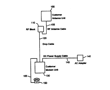
between outdoor and indoor units. Hence, an RF block 110 is provided which is
typically mounted on the exterior of a subscriber's premises, preferably the
RF block
110 being mounted in proximity to a customer antenna unit 100 used to transmit
and
receive wireless telecommunications signals. The customer antenna unit 100 is
then
connected to the RF block 110 via an RF antenna cable 105. Although the RF
block
110 and customer antenna unit 100 are illustrated in Figure 4 as separate
units
connected by an antenna cable 10~, it will be appreciated by those skilled in
the art
that, if desired, the antenna unit can be integrated within the RF block 110
so as to
provide a single unit for mounting on the exterior of the subscriber's
premises.
In preferred embodiments, all of the electronic circuitry which is dependent
on
the operating frequency band used for the wireless communications between the
subscriber terminal and the central terminal is located within the RF block
110, the
purpose of the RF block 110 being to translate received downlink signals from
the RF
frequency to a standard intermediate frequency suitable for transmission to
the
customer modem unit 130, and similarly to translate received signals from the
customer modem unit 130 at a standard intermediate frequency into an RF uplink
signal for transmission from the customer antenna unit 100.
The RF block 110 and the customer modem unit 130 are connected via a drop
cable 120, the drop cable 120 preferably being provided by a coaxial cable.
The
customer modem unit 130 incorporates a CDMA modem operating at a fixed
intermediate frequency, and also includes the electronics required to
interface to the
one or more items of telecommunications equipment connected to the subscriber
CA 02311470 2000-OS-19
WO 99127732 PGT1GB98/03416
terminal. In preferred embodiments, the customer modem unit 130 is located
within
the subscriber's premises, for example close to the items) of
telecommunications
equipment. Hence, an item of telecommunications equipment 1 SO is connected to
the
customer modem unit 130 via a lead 15~. Further, the customer modem unit is
5 preferably connected to an AC adaptor 140 via a DC power supply cable 145,
the AC
adaptor 140 providing power to the customer modem unit 130.
Under the relevant legislation in many countries, it is often required that
telecommunications equipment operating via wireless links be provided with a
separate
source of power so that the telecommunications equipment can be used in an
10 emergency, even in the event of a power cut disabling the main source of
power to
the equipment. Hence, in preferred embodiments a battery backup unit is
incorporated
within the customer modem unit, for example a lead acid battery.
The circuitry within the RF block 110 will also require a source of power in
order to operate, and in preferred embodiments, the necessary power is
provided from
15 the customer modem unit 130 via the drop cable 120.
The architecture illustrated in Figure 4 enables a number of cost reductions
to
be made. For example, if the antenna 100 were to be integrated within the RF
block
110, then this would result in a neat packaging, but would require that the
antenna be
designed for universal deployment. This typically means designing an antenna
with
as high a gain as possible, contributing to expense. However, by retaining the
antenna
100 as a separate unit to the RF block 110, then the subscriber terminal can
be
equipped with a lower cost "regular" specification antenna which would be
suitable for
most deployments. Then, in situations where signal strength is unusually low,
the
subscriber terminal could optionally be equipped with a high gain antenna, for
example as a cost option to the subscriber. This approach increases
flexibility, and
enables a lower cost antenna to be used for most situations where that antenna
will be
sufficient.
The subscriber terminal of preferred embodiments will preferably be provided
with an antenna which is significantly smaller and lighter than the combined
antenna/customer radio unit used in the subscriber terminals of the prior art.
By using
a smaller and lighter antenna, fewer restrictions on location and mounting
hardware
CA 02311470 2000-OS-19
WO 99127732 PCT1GB98/03416
16
are present. For example, since the unit is smaller than that used in prior
art
subscriber terminals, it is more suitable for pole mounting above the roof
line. At
higher elevations, the increased receive signal will offset any lower antenna
gain
resulting from the use of a smaller antenna.
The antenna design and/or technology choice changes with frequency. When
designing for a new operating frequency band, changes in the antenna design
are likely
to result in changes in the subscriber terminal mechanical design and/or
packaging,
resulting in a large number of manufacturing variants. If the subscriber
terminal
mechanics cannot be changed, then antenna performance may be compromised.
However, the subscriber terminal of preferred embodiments of the present
invention
allows the option of providing a readily available antenna for a new operating
frequency band until volume of sales justifies altering the design of the
subscriber
terminal. Hence, it will be possible to readily provide a subscriber terminal
that will
operate in a different RF operating frequency band.
Apart from the above described cost reductions that arise from the RF
block/antenna architecture, a number of other cost reductions can be realised
as a
result of employing the architecture illustrated in Figure 4. For example,
since all of
the operating frequency band sensitive components are preferably restricted to
the RF
block 110, then the modem within the customer modem unit 130 operates at a
standard intermediate frequency for all RF operating frequency bands. Hence,
the
customer modem unit 130 may be manufactured in large volumes regardless of
which
operating frequency band the equipment will operate in. Subsequent design
modifications would then preferably be restricted to the RF block 110.
The drop cables used in the prior art subscriber terminal, such as that
illustrated
in Figure 1, typically would comprise a high specification screened five-pair
cable.
This cable is expensive, as are the connectors required to terminate the cable
and
protection networks. However, in preferred embodiments of the present
invention, a
simple coaxial cable is used to carry power, control and IF uplink and
downlink
signals between the RF block 110 and the customer modem unit 130, thereby
removing the need for costly cable and connectors.
In preferred embodiments, the customer interface and radio modem functions
CA 02311470 2000-OS-19
WO 99/Z7732 PCT/GB98I03416
17
are separated within the customer modem unit. A radio modem card is provided
which is designed to operate at a standard IF, and to present a fixed
interface to a
customer interface card. The customer interface card is then dependent on the
particular items) of telecommunications equipment supported by the subscriber
terminal. By this arrangement, the radio modem card will operate with any
customer
interface variant, and so the radio modem card can be manufactured in high
volume
with a design that is independent of the telecommunications equipment
supported by
the subscriber terminal, thereby providing cost savings. Preferably, customer
specific
variants of the customer interface card may be developed as and when required,
and
such design changes in the customer interface card will not require re-
qualification of
the radio modem card. Furthermore, any cost reduction of the radio modem card
arising through higher integration of the components will not in preferred
embodiments require design changes in the customer interface card.
In preferred embodiments, the AC adaptor 140 used to supply power to the
subscriber terminal is a low cost universal AC adaptor supplying 18V DC to the
customer modem unit 130 and the RF block 110. The customer modem unit 130 also
in preferred embodiments incorporates a low cost 20W hr lead acid battery for
backup
in the event of a mains failure. Power dissipation and hence battery cost are
reduced
in preferred embodiments by arranging logic circuitry to operate from 3.3V
where
possible, and for all circuitry not required when the RF link is not in use to
be
powered down, including RF transmit, IF transmit, baseband transmit and codec
circuitry. Further, the processors preferably exploit power saving modes of
operation.
The low power dissipation results in further cost reductions by easing thermal
management requirements. Further, since the outdoor RF block enclosure is
smaller
and lighter than the prior art customer radio unit, the mounting hardware can
be
lighter duty, and hence cheaper. Further, the indoor customer modem unit
contains
a significant proportion of the processing circuitry, and lower cost plastics
and
assembly methods can be used than were typically'required for the customer
radio unit
of prior art subscriber terminals, since the indoor environment requires less
mechanical
integrity.
Having discussed some of the benefits arising from employing an architecture
CA 02311470 2000-OS-19
wo ~m~3z rc~ricB9sio3oi6
is
as set out in Figure 4, the RF architecture of the subscriber terminal of
preferred
embodiments will now.be discussed in more detail. As previously discussed with
reference to Figure 4, the RF architecture is split between indoor electronics
within the
customer modem unit 130 that up/down-converts baseband information to a
standard
IF band, and outdoor electronics within the RF block 110 that performs the
up/down-
conversion to RF.
Figure 5 is a diagram illustrating the arrangement of components within the RF
block 110 used to convert signals between IF and RF. Considering first an RF
signal
received by the subscriber terminal, this received signal will be passed via
the antenna
202 to an RF filter 200 which is arranged to only let signals with frequencies
within
a predetermined frequency range to be output over path 204. The RF filter 200
and
RF filter 210 together form a duplex filter, filter 210 being of a type which
will allow
transmit signals on path 206 to be output to the antenna 202 whilst preventing
received
RF signals being passed from the antenna 202 to the path 206. Similarly, the
RF filter
200 is of a type which prevents transmit signals on path 206 being propagated
onto
the path 204 whilst allowing received signals via the antenna 202 to be passed
to the
path 204. In preferred embodiments, the RF filter 200 will allow received
downlink
signals with centre frequencies ranging from 3511.75 to 3550.25MHz to be
passed
through the filter, whilst the RF filter 200 will allow uplink signals with
centre
frequencies ranging from 3411.75 to 3450.25MHz to be passed through the
filter.
Hence, in preferred embodiments, a received RF signal at the antenna 202 will
be passed through the RF filter 200 over path 204 to a switch 240. In normal
operation, the switch 240 is arranged to pass the received signal to a low
noise
amplifier (LNA) 230. However, in a calibration mode of operation, which will
be
discussed in more detail later, the switch 240 can be used to block out any
signals
received by the antenna 202, and instead pass a signal from a calibrated noise
source
245 to the LNA 230. '
Once the signal has passed through the switch 240, it is amplified by the LNA
230 and further amplifier 235 before being passed to an attenuation network of
resistors 212, 214, 216. These three resistors 212, 214 and 216 act in
combination to
attenuate the received signal prior to it being passed on to a filter 250. It
is advisable
CA 02311470 2000-OS-19
WO 99127732 PCTlG898/03416
19
to include such attenuation circuitry 212, 214, 216 so as to ensure that the
subsequent
circuitry is not exposed fo a signal having a higher power level than those
components
are designed for. Such a high powered signal may, for example, be received at
the
antenna 202 if the subscriber terminal is placed particularly close to the
central
terminal with which it is arranged to communicate. The attenuation circuitry
212, 214
and 216 then serves to ensure that this initially received signal is
attenuated prior to
its propagation through the rest of the processing circuitry. If,
subsequently, it is
determined that the attenuation performed by the resistors 212, 214 and 216 is
unnecessary, then a control signal C2 can be passed to a switch 220 to turn
the switch
on and thereby bypass the attenuation circuitry.
Once the signal has passed through the attenuation circuitry 212, 214, 216 or
switch 220, it is passed to a filter 250. The filter 250 is arranged to remove
wide
band noise generated by the LNA 230, by only allowing signals within a
specified
bandwidth centred on a predetermined frequency to pass through the filter. In
preferred embodiments, the bandwidth allowed through the filter is 42MHz,
centred
on a frequency of 3~31MHz, i.e. the middle of the frequency range for downlink
signals passed from the antenna 202 through the RF filter 200.
The signal output by the filter 250 is then passed to a mixer 260 via a
matching network of resistors 252, 254, 256. The matching network serves to
match
the impedance at the output of the filter 250 with the impedance of the input
to the
mixer 260. The mixer 260 is also arranged to receive an input from an RF
synthesizer
280, the RF synthesizer 280 being controlled by configuration logic 285. In
preferred
embodiments, the signal output by the RF synthesizer 280 to the mixer 260 is
at a
frequency of 2596MHz. Based on two input signals at frequencies f, and f,, a
mixer
such as mixer 260 will produce signals at two output frequencies, namely f, +
f, and
f, - f=.
Signals output by the mixer 260 are then amplified by an amplifier 270 before
being received by a duplex filter comprising filter 290 and filter 295. In
preferred
embodiments, the filter 290 is arranged to remove the f, + fz component of the
signals
produced by the mixer 260, and to only allow the f, - f, component to be
passed
through to the drop cable 120. Further, the filter 295 is arranged to prevent
any
CA 02311470 2000-OS-19
WO 99/Z7732 PGT/GB98/03416
signals from the amplifier 270 being propagated through to the path 305.
Hence, in
preferred embodiments, the intermediate frequency used to transmit received
signals
via the drop cable between the RF block 110 and the customer modem unit 130
comprises the f, - f, component generated by the mixer 260 from the signals
received
5 from both the RF synthesizer 280 and the filter 250.
Considering now signals to be transmitted from the antenna 202, signals at an
intermediate frequency in the range of 815.75 to 854.25MHz are preferably
generated
by the customer modem unit 130 and transmitted over the drop cable 120, where
they
are then received by the duplex filter 290, 295. The filter 295 is arranged to
10 propagate such signals over the path 305 to an amplifier 310, whilst the
filter 290
prevents such signals from being passed back through the circuitry described
earlier.
The amplifier 310 amplifies the signals and then passes them to the mixer 320
via a
matching network 312, 314, 316. This matching network matches the impedance at
the output of the amplifier 310 with the impedance at the input of the mixer
320.
15 The mixer 320 also receives an input from the RF synthesizer 280, in
preferred
embodiments this signal being at the same frequency as the signal transmitted
from
the RF synthesizer 280 to the mixer 260. The f, + f~ and f, - f, components
generated
by the mixer 320 are then passed via another matching network 322, 324, 326
and an
amplifier 330 to a filter 340.
20 The filter 340 is arranged to only allow signals in a bandwidth of 42MHz
centred on a predetermined frequency to be passed through the filter 340, in
preferred
embodiments this predetermined frequency being 3431MHz so as to remove the f, -
f2 component produced by the mixer 320. Subsequent amplification of the signal
is
performed by amplifiers 350 and 360 to counteract the loss of the filter 340,
prior to
the signals being output via the switch 370 to the filter 210, and from there
to the
antenna 202 for transmission. During normal operation, the switch 370 is
arranged
to pass the signals output by the amplifier 360 to the RF filter 210. However,
during
installation calibration procedures, the switch 370 can be switched such that
the signal
is earthed via the resistor 380 to prevent transmission of a test signal
generated during
calibration.
Further, the signal output by the amplifier 360 to the switch 370 is coupled
via
CA 02311470 2000-OS-19
WO 99/Z7732 PCT1GB98/03416
21
a coupler 385 to a diode 390. This provides an indication 'P' of the transmit
power
of the signal, this indication 'P' being provided to a serial communications
controller
410 within the RF block 110, which then passes that information via the drop
cable
120 to the customer modem unit 130.
~ The circuitry illustrated in Figure 5 is intended for use in a subscriber
terminal
using the CEPT SE19~ Recommendation for wireless telecommunications, where the
duplex spacing is 100MHz. However, other duplex spacings, such as 175MHz and
94MHz, can easily be accommodated by incorporating an additional fixed
frequency
synthesizer.
In order for the automatic frequency control (AFC) loop to operate correctly,
the RF synthesizer 280 must be phase locked to a l3MHz frequency reference
located
in the customer modem unit 130. This is achieved by sending a l3MHz tone up
the
drop cable from the customer modem unit, this tone then being isolated using a
filter
400. This filter 400 is arranged to allow signals within a bandwidth of SOKHz
and
centred on a frequency of l3MHz to be received by the RF synthesizer 280.
Further, certain control signals can be passed between the customer modem unit
130 and the RF block 110 via the drop cable. To facilitate this, the serial
communications controller 410 is provided within the RF block 110, which is
arranged
to transmit and receive signals centred on a frequency of 455KHz. A filter 420
is
used to isolate signals within a bandwidth of 20KHz and centred on a frequency
of
455KHz that are passed over the drop cable from the customer modem unit 130
for
subsequent processing by the serial communications controller 410. Further,
signals
emitted by the serial communications controller 410 at a frequency of 455KHz
will
be passed through the filter 420 and over the drop cable to the customer modem
unit
130. Hence, the serial communications controller 410 allows for bidirectional
communications with the CDMA modem in the customer modem unit 130. The
communications controller amplitude modulates a 455KHz Garner with binary
data.
In preferred embodiments, the data transmitted from the RF block 110 to the
CMU
130 comprises transmit power level (P) only. However, preferably the data
transmitted from the customer modem unit 130 to the RF block 110 may comprise
the
following:
CA 02311470 2000-OS-19
WO 99/Z9732 PCT/GB98/03416
22
1. Transmit on/off control (C1);
2. Transmit calibrate control (C4);
3. Receive calibrate control (C3);
4. Receive gain trim (loud switch) (C2); and
5. Receive signal strength indication (used in installation mode).
The above control signals C 1 to C4 are then output by the serial
communications controller 410 to the relevant components within the RF block 1
I0,
as illustrated in Figure S. Further, the receive signal strength indication
may be used
to drive LEDs 430 provided on the RF block 110 so as to provide a visual
indication
of the received signal strength, which, as will be discussed in more detail
later, is
useful during installation. Alternatively, or additionally, the receive signal
strength
indication may be passed to a DAC 440 to generate an analogue signal at an
output
port of the RF block 110. A device such as a voltmeter may then be connected
to the
output port to receive a signal indicative of the received signal strength.
In preferred embodiments, the power required to operate the RF block 110 is
received via the customer modem unit 130 over the drop cable 120. A DC-DC
converter 450 is provided within the RF block 110 to process the received
power
signal in order to generate a regulated voltage for supply to the circuitry
within the RF
block.
The customer modem unit 130 will now be discussed in more detail with
reference to Figures 6 and 7. As illustrated in Figure 6, the customer modem
unit 130
comprises a radio modem card 500 which is connected to the drop cable 120, the
radio
modem card 500 communicating with the RF block 110 via the drop cable 120 at
an
intermediate frequency. The radio modem card 500 incorporates all of the
functions
required to implement the baseband and IF parts of the CDMA modem. As
mentioned
earlier, the radio modem card 500 is designed as a generic modem to be
manufactured
in high volume independent of the customer interface. The interface to the
customer
interface card 510 is designed to support all anticipated applications,
including 1 to 4
line POTS, basic rate ISDN and D128 data. A more detailed description of the
radio
modem card will be provided later with reference to Figure 7B.
The customer interface card 510 is connected to the radio modem card 500,
CA 02311470 2000-OS-19
WO 99127732 PCT/GB98/03416
23
and incorporates the following functions:
1. A CPE interface, one or two line POTS, or ISDN. Preferably, the POTS CPE
interface uses a programmable digital signal processor (DSP) to implement
voice compression, tone generation and detection. Line hybrid balance and
gain trim may also be implemented by a DSP, but alternatively could be
implemented with external circuitry;
2. A microcontroller with nvo full software images held in FLASH of software
used to control the customer interface card, downloadable over the air or via
a Local Access Terminal (LAT) port. A software image is a specific instance
of a piece of software, and providing two software images allows one to be
active whilst the other is in standby, thereby allowing the standby image to
be
updated whilst the active image is running;
3. A Local Access Terminal (LAT) port;
4. A reset switch;
5. An interface to the radio modem card 500;
6. A switching power converter, a battery charger and a backup switch;
7. An LED panel driver; and
8. A smartcard interface.
As illustrated in Figure 5, the customer modem unit 130 also incorporates a
single lead-acid battery 530, this battery having a nominal output voltage of
12 volts
for power backup. In preferred embodiments, battery access is via a removable
panel
on the customer modem unit. Flying or captive leads may be used to connect the
battery to the customer interface card S 10, which incorporates the battery
charging
circuitry and switching that is activated in the event of DC input failure.
An LED panel 520 is also provided within the customer modem unit 130 in
preferred embodiments, this LED panel being used to provide status information
to the
user. In preferred embodiments the following indications are provided:
CA 02311470 2000-OS-19
WO 99/27932 PCT/GB98/t13416
24
PositionType FunctionOff Flash On (Red)On
(Green)
1 Red Fault Unit OK Unit requiresFault
configuration
2 Green Power No power Switched - DC input
to
battery OK
S 3 Bi-colourLink No link - Link Downlink
in
use OK
It will be appreciated by those skilled in the art that an LCD panel could be
used instead of the LED panel.
Having described the main elements of the customer modem unit 130, the
circuitry within the radio modem card 500 used to perform IF processing will
now
be discussed in detail with reference to Figure 7A.
Considering first an IF signal transmitted to the radio modem card 500 from
the RF block 110 via the drop cable 120, this signal will be received by the
duplex
filter 600, 605. The duplex filter is arranged such that the filter 600 will
allow the
1 S IF signal to pass to the path 604, whilst the filter 605 will prevent the
signal passing
to the path 602. Hence, the received signal is passed via the path 604 to a
variable
attenuator 640, prior to being passed on through an amplifier 630 to a mixer
650.
The variable attenuator 640 is controlled by the CDMA modem within the radio
modem card (which will be discussed in more detail later with reference to
Figure
7B), and is used to compensate for the losses introduced by the drop cable
120.
The mixer 650 also receives a signal from a first IF synthesizer 665, which
is referenced back to a l3MHz frequency reference oscillator 700. The
oscillator 700
is controlled by the CDMA modem within the radio modem card 500 as part of an
AFC loop. The first IF synthesizer 665 may be programmed to any one of twelve
2S 3.SMHz channels within the 42MHz band spanning the range 815.75 to
854.2SMHz,
and hence performs RF channel selection. The f, + f, and f, - f, components
then
generated by the mixer 650 are amplified by an amplifier 655 before being
passed to
a SAW filter 660. The SAW filter is arranged to allow signals in a bandwidth
of
CA 02311470 2000-OS-19
WO 99/Z7732 PG"f/G898/03416
3.5MHz centred on a frequency of 100MHz to be passed through the filter, and
hence
the SAW filter 660 removes the f, + f~ component produced by the mixer 650.
The
3.5MHz SAW filter 660 in effect isolates the RF channel selected by the first
IF
synthesizer 665.
5 The output from the SAW filter 660 is then passed via a matching network
672, 674, 676 to a variable amplifier 680, this amplifier 680 performing
automatic
gain control (AGC). The signal is then passed to the demodulator circuit 690,
which
performs quadrature demodulation to baseband I and Q components. The I
component is then passed via an amplifier 694 to a CDMA demodulator within the
10 radio modem card 500, whilst the Q component is passed via an amplifier 692
to the
CDMA demodulator.
A more detailed illustration of the circuitry 690 is provided in Figure 8A. As
can be seen, the signal from the AGC amplifier 680 is divided into two
separate
signals, one received by the mixer 702 and one received by the mixer 704. A
"divide
15 by 4" circuit is arranged to generate four 100MHz signals, phase shifted by
90° from
each other, from a 400MHz signal generated by a second IF synthesizer 695,
this
second IF synthesizer also being referenced back to the l3MHz frequency
reference
oscillator 700. The mixer 702 receives one of these 100MHz signals and then
uses
its two input signals to generate an "I" component. Meanwhile, a second 100MHz
20 signal phase shifted by 90° is input to the mixer 704, and the mixer
704 then creates
the "Q" component from the phase shifted 100MHz signal and from the other
input
signal.
Considering now signals to be transmitted by the subscriber terminal, the I
and
Q components of the transmit signal are first passed through filters 730 and
735,
25 respectively. These two filters have a bandwidth of 2MHz in preferred
embodiments,
and serve to extract the fundamental from the digitally generated signals. The
output
from the filters 730 and 735 are then amplified by the amplifiers 740 and 745,
respectively, before being passed to the circuitry 750. The circuitry 750 is
illustrated
in more detail in Figure 8B. As illustrated in Figure 8B, the I component of
the
signal is received by a mixer 752, and the Q component of the signal is
received by
a mixer 754. Both mixers also receive a signal from the first IF synthesizer
665,
CA 02311470 2000-OS-19
WO 99/27732 PCT/GB98~3416
26
although the signal received by the mixer 754 is phase shifted by 90°
prior to being
received by the mixer 754. As mentioned earlier, the first IF synthesizer 665
operates from 815.75 to 854.25MHz and can be programmed to any one of twelve
3.5MHz channels within the 42MHz band in order to perform RF channel
selection.
The signals generated by the mixers 752 and 754 are then passed to the
combiner 756
where they are combined into a single signal.
The combined signal is then passed via a matching network 762, 764, 766 to
an amplifier 775. The signal output by the amplifier 775 is then passed
through a
variable attenuator 780, and a matching network 782, 784, 786. Then the signal
is
again passed through a variable attenuator 795 before being passed to an
amplifier
810.
Then the signal is passed through a variable attenuator 815 prior to being
passed over path 602 to the duplex filter 600, 605. The variable attenuator
815 is
arranged to compensate for the losses that will be introduced by the drop
cable 120.
The filter 605 is then arranged to cause the signal on path 602 to be output
on to the
drop cable 120, whilst the filter 600 prevents that signal from being
propagated on
to the path 604.
As also illustrated in Figure 7A, the l3MHz reference frequency generated by
the oscillator 700 is passed through a filter 825 having a bandwidth of SOKHz
centred
on a frequency of l3MHz. The output of the filter 825 is then passed to the
drop
cable 120 for transmission over the cable to the RF block 110. As mentioned
earlier,
in order for the AFC loop within the RF block 110 to operate correctly, the RF
synthesizer 280 within the RF block 110 must be phase locked to the l3MHz
frequency reference generated by the oscillator 700 in the customer modem unit
130.
By sending this l3MHz tone up the drop cable, the required phase locking of
the RF
synthesizer can be achieved.
Further, as illustrated in Figure 7A, a serial communications controller 830
is provided to allow low rate bidirectional communications with the RF block
110,
the communications controller amplitude modulating a 455KHz carrier with
binary
data. This signal is then passed via a filter 840 having a bandwidth of 20KHz
centred
on a frequency of 455KHz, and from there the signal is passed to the drop
cable 120.
CA 02311470 2000-OS-19
WO 99/27732 PCT/GB98/03416
27
The filter 840 also serves to isolate any control signals issued by the RF
block 110
and passed over the drop cable 120 to the radio modem card 500. As mentioned
earlier, in preferred embodiments the RF block 110 may for example issue a
control
signal identifying the transmit power level. The filter 840 then isolates that
signal,
and passes it on to the serial communications controller 830.
Also, the radio modem card 500 is arranged to provide DC power to the drop
cable 120 for transmission to the RF block 110 to power the RF block
components.
The CDMA modem within the radio modem card 500 which is used to control
the circuitry of Figure 7A will now be described in more detail with reference
to
Figure 7B. The CDMA modem of preferred embodiments essentially consists of a
Digital Signal Processor (DSP) 855 which 'is connected to both a CDMA
modulator
850 and a CDMA demodulator 860. The RXI and RXQ signals generated by the
demodulator circuit 690 are passed through ADCs 868 and 870, respectively,
prior
to being received by the CDMA demodulator 860.
The CDMA demodulator 860 then performs CDMA demodulation under the
control of the DSP 855, and outputs the received data (Rx data) and received
clock
(Rx clock) signals to the customer interface card 510. Further, the CDMA
demodulator 860 generates a synchronisation (Sync) signal used to synchronise
various circuitry within the customer modem unit 130. This Sync signal is
output to
the customer interface card 510 and is also provided to the CDMA modulator
850.
The CDMA demodulator receives data (Tx data) and clock (Tx clock) signals
from the ST's connected telecommunications equipment via the customer
interface
card 510. This data is then used by the CDMA modulator 850 to generate CDMA
modulated I and Q signals under the control of the DSP 855, these signals
being
passed through respective DACs 862 and 864 to generate the TXI and TXQ signals
input to the circuitry of Figure 7A.
The DSP 855 has a host processor interface with the customer interface card
510 to enable communications with the microcontroller on the customer
interface card
to take place. Further the DSP 855 can receive signals from the CDMA
demodulator
860, such as details of signal strength used by the DSP during installation of
the ST,
this being described in more detail later.
CA 02311470 2000-OS-19
WO 99/27732 PCT/GB98/03416
28
The DSP 855 is arranged to generate the various signals used to control the
circuitry of Figure 7A. Hence, the DSP outputs signals to a multiple DAC 866,
which
then outputs the AFC signal input to the oscillator 700 to perform automatic
frequency control, and outputs the TX_GC and RX GC gain control signals input
to
the variable attenuators 780, 795 and the variable amplifier 680 to control
gain of the
transmit and receive signals during normal operation.
Further, the DSP 855 generates the transmit enable (TX EN) signal used to
control the circuitry 750, and amplifiers 775, 810 to allow transmission to
take place.
In addition, during calibration of the circuitry (eg. on installation), the
DSP 855
generates the TX COMP and RX-COMP signals used to control the variable
attenuators 815 and 640, respectively, to compensate for the losses incurred
by
transmission of the uplink and downlink IF signals over the drop cable 120.
This
process will be described in more detail later.
Finally, the DSP 855 is responsible for generating the various control signals
(SCC DATA) passed to the serial communications controller 830 for transmission
over the drop cable 120 to the RF block 110. Additionally, the DSP 855 will
receive
via the serial communications controller 830 any control signals issued by the
RF
block 110, for example the transmit power level indication 'P'.
Having described the circuitry of the RF block 110 and the radio modem card
500, the signals passed between these two units via the drop cable 120 will
now be
discussed in more detail with reference to Figure 9, which illustrates the
spectrum
utilisation for the drop cable. As mentioned earlier, the drop cable 120
preferably
comprises a two conductor coaxial cable carrying the following signals between
the
radio modem card 500 and the RF block 110:
1. Uplink IF spread-spectrum signal;
2. Downlink IF spread-spectrum signal;
3. l3MHz frequency reference;
4. 455KI~z carrier data link; and
5. DC power, preferably 10 to 20 volts.
As mentioned earlier, elements of the RF block 110 are in preferred
embodiments controlled by the CDMA modem on the radio modem card 500. Digital
CA 02311470 2000-OS-19
WO 99/Z7~32 PCT/GB98~3416
29
data is pulse position modulated on to a 455KHz carrier, this frequency being
chosen
due to ready availability of ceramic filters and resonators and because it is
not
harmonically related to the l3MHz frequency reference signal (13/0.455 =
28.5714).
In preferred embodiments, each data bit is sent using a line code comprising a
start
bit, data bit and stop bit. The correlation between the data bit and the line
code in
preferred embodiments is as follows:
Data bit Line code
0 100
1 110
Preferably data is sent in packets as follows:
Packet Element Number of Bits
Sync Header 3
Address 1
Payload 8
Parity 1
In preferred embodiments, the packets are time division multiplexed every
30ms. The CMU controller preferably acts as a protocol master, initiating
communications every 30ms. The header preferably comprises a fixed sequence,
say
001. Further, the address is typically set to zero for communication with the
RF
block 110, and a non-zero address is used for communications with equipment
other
than the RF block, for example a receive signal strength meter. The payload
preferably comprises 8 bits and the packet is error protected with a single
parity bit.
Figure 10 provides a more detailed illustration of the serial communications
controller 830 and the filter 840 illustrated in Figure 7. An oscillator 900
is arranged
to produce a carrier signal at 455KHz. Control inputs passed to the serial
CA 02311470 2000-OS-19
WO 99/Z7732 PCT/GB98/03416
communications controller 830 then cause control data to be output from the
serial
communications controller to a switch 910, the switch 910 pulse position
modulating
that data on to the 455KHz carrier signal. This signal is then passed to the
filter 840
which allows a bandwidth of 20KHz centred on 455KHz to be output to the drop
5 cable 120.
For a control signal issued by the RF block 110, the filter 840 will isolate
that
signal and then pass it to the diode 920 which will rectify the signal. The
rectified
signal is then passed to a low pass filter 930 which removes the 455KHz
carrier
signal. The output from the filter 930 is then passed to a comparator 940
where the
10 signal is compared with a threshold voltage to produce at the output a
digital signal
for passing to the serial communications controller 830. The serial
communications
controller then uses this signal to create parallel control outputs.
The architecture illustrated in Figure 10 is also applicable to the serial
communications controller 410 and the filter 420 of the RF block 110
illustrated in
15 Figure 5. The serial communications controller within the RF block 110 may
also
handle configuration of the RF synthesizer 280 at power-up.
Having described the subscriber terminal of preferred embodiments in detail,
the installation of the subscriber terminal will now be discussed. Important
aspects
of the installation process are unit configuration and antenna alignment.
20 Before an ST becomes operational, configuration data must be entered into
the
unit. As an example the following minimum information may be required:
1. RF channel number;
2. PN code; and
3. An ST identifier (preferably a six digit number).
25 Two options exist for entering this data. Firstly, if a LAT port is fitted,
as
is the case for the customer modem unit 130 of preferred embodiments
illustrated in
Figure 6, then an external terminal may be used to configure the unit. This
technique
would generally be used for STs with ISDN or D128 interfaces. An alternative
approach is to use a telephone connected to the subscriber terminal, such an
approach
30 typically being used if the subscriber terminal is to be used for POTS
signalling. A
technique that may be used for this purpose is described in detail in the
patent
CA 02311470 2000-OS-19
wo ~n~~3z rcncB~om6
31
application GB-A-2,301,738.
Once the necessary configuration data has been entered, then in preferred
embodiments a calibration step is performed to calibrate the ST with respect
to the
signal losses introduced by the drop cable. The technique used in preferred
embodiments to perform this calibration will now be described with reference
to
Figures 5, 7A and 7B.
Firstly, to calibrate the downlink path to compensate for losses introduced by
the drop cable, the DSP 855 generates the receive calibrate control signal C3
on the
SCC DATA channel, which is then passed by the serial communications controller
830 over the drop cable 120 to the serial communications controller 410 in the
RF
block 110. This causes the serial communications controller 410 to issue the
C3
signal to the switch 240, to cause the calibrated noise source 245 provided in
the RF
block 110 to be switched into the downlink path. Preferably, this calibrated
noise
source produces additive white Gaussian noise at a predetermined power level.
This
noise signal is then passed through the receive path circuitry of Figure 5,
over the
drop cable 120, and through the receive path circuitry of Figure 7A to produce
RXI
and RXQ components which are output to the CDMA demodulator 860 of the CDMA
modem illustrated in Figure 7B.
Here, predetermined criteria are stored which the calibrated noise source
should exhibit when received by the CDMA demodulator 860 if the losses of the
drop
cable have been compensated for. By comparing the actual received noise signal
with
the predetermined criteria, the CDMA demodulator can determine whether the
setting
of the variable attenuator 640 should be incremented or decremented. One
example
of the predetermined criteria which may be stored is the frequency with which
signals
2~ outside a certain number of standard deviations from the peak of the
Gaussian signal
should be received. Since the noise signal is digitised prior to being
received by the
CDMA demodulator 860, the CDMA demodulator can be arranged to keep a count
of the number of times the signal is outside the determined number of standard
deviations, and notify the DSP 855 if the number exceeds a certain threshold,
thereby
indicating that the setting of variable attenuator 640 should be altered.
When the DSP 855 receives a signal from the CDMA demodulator 860
CA 02311470 2000-OS-19
WO 99/Z7732 PGT/GB98/03416
32
identifying that the setting of the variable attenuator 640 should be altered,
it
generates a RX COMP signal for outputting to the variable attenuator 640 to
alter its
setting. By appropriate setting of the variable attenuator 640, the losses
introduced
by the drop cable in the receive path can be compensated for.
5 To calibrate the uplink path to compensate for losses introduced by the drop
cable, the DSP 85~ is arranged to instruct the CDMA modulator 850 to generate,
in
preferred embodiments, a calibrated noise signal for transmission through the
transmit
path circuitry of Figure 7A and Figure 5. To avoid the noise signal being
transmitted
from the antenna 202, the DSP 855 also generates a control signal C4 on the
10 SCC-DATA output, which is passed via the serial communications controller
830 of
the radio modem card 500 over the drop cable 120 to the serial communications
controller 410 in the RF block, thereby causing the serial communications
controller
410 to issue the C4 signal to the switch 370 to earth the transmit signal.
However, the coupler 385 in the RF block 110 still receives the transmitted
15 noise signal, and hence provides an indication 'P' of the transmit power of
the signal.
This indication ' P' is provided to the serial communications controller 410
within the
RF block 110, which then passes that information via the drop cable 120 to the
serial
communications controller 830 in the radio modem card 500. This data is then
passed
to the DSP 855 via the SCC DATA channel, and the DSP compares the indication
20 P with a predetermined value to determine whether the setting of the
variable
attenuator 815 should be altered. If alteration is necessary, then the DSP
outputs a
D
suitable TX COMP signal to the variable attenuator 815 to alter its setting.
By this
approach, the losses introduced by the drop cable in the transmit path can be
compensated for.
25 Once the necessary calibration steps have been performed, then the antenna
100 of the subscriber terminal is in preferred embodiments aligned so that it
is
pointing towards the central terminal with which it is intended to
communicate. Since
the antenna is typically mounted at an elevated position on the exterior of
the
subscriber's premises, then the engineer will generally have to climb up to
the
30 mounting location of the antenna and manually align the antenna unit.
Where a LAT port is fitted to the subscriber terminal, an external terminal
CA 02311470 2000-OS-19
wo ~m~3z rc'ncs9siom6
33
may be used to monitor receive signal strength and act as a guide for antenna
panning. However, since the LAT port, if any, will typically be provided at
the
customer modem unit 130 located inside the subscriber's premises, then such an
approach is very cumbersome if carried out by a single engineer, and so
typically
involves two engineers, one for adjusting the antenna, and one for monitoring
the
receive signal strength.
In accordance with preferred embodiments of the present invention, a number
of simplified options are available for aiding antenna alignment. All of these
options
require that the subscriber terminal be placed in a special mode of operation
which
inhibits normal operation. This could for example be achieved by entering a
special
code into the subscriber terminal following unit reset. The unit would then
remain
in antenna alignment mode to enable the installation to be completed.
The receive signal strength is measured on de-spread data in the CDMA
demodulator 8b0 within the customer modem unit 130, where the true signal
power
can be distinguished from access noise. One option for removing the
requirement for
an external terminal to be fitted via the LAT port is to use the customer
modem unit
LED/LCD panel to indicate receive signal strength. However, this would still
typically require two engineers to perform the installation.
Hence, an alternative option is to incorporate LEDs into the RF block 110 to
indicate receive signal strength, as was discussed earlier with reference to
Figure 5
Since the RF block 110 is likely to be located very close to the antenna unit
100, and
indeed in some implementations both the RF block 110 and the antenna unit 100
will
be incorporated into the same physical device, then the engineer that is
adjusting the
antenna can also view the LED indication on the RF block. However, as
mentioned
earlier, the receive signal strength is preferably measured in the CDMA
demodulator
within the customer modem unit 130. Hence, in preferred embodiments, the
receive
signal strength as determined by the CDMA demodulator is then output by the
DSP
855 on the SCC DATA output and transmitted back up the drop cable 120 via the
serial communications link, and subsequently displayed on the LEDs of the RF
block
110.
As illustrated in Figure 5, as an alternative, or in addition, to the LEDs, a
CA 02311470 2000-OS-19
wo ~m~z rcrics9srom6
34
DAC 440' can be provided in the RF block 100 to generate at an output port of
the
RF block an analogue received signal strength indication (RSSI). Then, a
device such
as a voltmeter can be attached by the installation engineer to provide an
indication of
received signal strength.
Further, since in preferred embodiments the ST has already been calibrated,
prior to the antenna alignment process being performed, to compensate for
losses
introduced by the drop cable, the LEDs or voltmeter can be calibrated to
provide a
direct reading of received signal strength to the installation engineer.
Yet another alternative approach, depicted in Figure 11, is to place a receive
signal strength meter 960 in line with the drop cable 120. As before, the
receive
signal level is transmitted up the RF block cable using the serial
communications link,
but in this instance is intercepted by the meter. The signal strength level is
then
displayed on an LED or LCD panel provided by the signal strength meter. When
alignment is complete, the meter is removed and the drop cable fitted to the
RF block
110.
The main advantage of providing either indication mechanisms in the RF block
or a separate meter connected to the cable in the vicinity of the RF block is
that the
signal strength can be evaluated near the RF block, thereby enabling the ST to
be
installed by a single person. Further, in preferred embodiments, the
indication can be
calibrated to give a direct indication of "fade margin", i.e. the amount of dB
variation
before the communication path is lost.
It will be appreciated by those skilled in the art that the actual device used
to
provide the indication of received signal strength is not important. Any type
of visual
or audible indication could be used as appropriate.
Although a particular embodiment has been described herein, it will be
appreciated that the invention is not limited thereto and that many
modifications and
additions thereto may be made within the scope of the invention. For example,
various combinations of the features of the following dependent claims could
be made
with the features of the independent claims without departing from the scope
of the
present invention.