Note: Descriptions are shown in the official language in which they were submitted.
CA 02311544 2000-OS-19
- WO 99/26806 PGT/GB98/03473
-1-
Controller for Battery-Operated Vehicle
The present invention relates to a power controller, for example a controller
for a
motor in a battery-operated vehicle. Such controllers typically have to switch
large
currents at low voltages (eg currents of the order of 500 A at 24 V or 48 V),
and
typically use control circuit comprising a bank of switching elements, and a
capacitor.
A first switching element may be a MOSFET transistor and a second switching
element a diode (i.e. a passive switching element); alternatively, both
switching
elements may be MOSFET transistors. It will of course be realized that such
controllers may also have application beyond battery-operated vehicles, in
other
situations in which large currents have to be controlled.
An object of at least the preferred embodiments of the present invention is to
minimize
the size and cost of such controllers.
According to one aspect of the invention there is provided a power controller,
comprising a plurality of switching circuits each consisting of a first
switching
element, a second switching element, and a capacitor, and a printed circuit
board
having the switching circuits arranged around an inner area of the board in a
partial
or complete loop, the inner area of the board and the area outside the loop
(the outer
area) being substantially solid tracking areas forming the sole connections to
the
switching circuits.
The inner area on both sides of the board and the outer area on at least one
side may
form the connections to the circuits.
The switching circuits may be arranged in four sets, each set parallel to a
respective
edge of the board.
Preferably the connectors to circuits are located substantially along a
diagonal of the
board, with the connectors to the two sides of the diodes located at opposite
corners
CA 02311544 2000-OS-19
WO 99/2b806 PCT/GB98/03473
-2-
of the inner areas of the board. The parts of at least one of the tracking
areas
adjacent to the circuits are preferably divided by isolating lines into
separate fingers
for the respective circuits.
According to another aspect of the invention there is provided a power
controller,
comprising a switching circuit consisting of a first switching element, a
second
switching element, and a capacitor, mounted on a printed circuit board with
the first
and second switching elements mounted on one face of the board and the
capacitor on
the other.
Preferably a heat sink is located between the switching elements to receive
heat
therefrom. There may be means mechanically fixing the switching elements to
each
other via the heat sink. Thus the switching elements may be clamped to the
heat sink,
preferably by a nut and bolt passing through lugs on the switching elements
and a
matching hole in the heat sink, which may be of bar-like configuration. There
may
be a plurality of switching circuits arranged in a row with a common heat
sink. A
heat dissipating element eg. a plate substantially parallel to the printed
circuit board
may be attached to the heat sink.
A controller embodying the invention will now be described, by way of example,
with
reference to the drawings, in which:
Fig. 1 is a simplified circuit diagram of a vehicle circuit for a series
motor, including
the controller;
Fig. 1A is a circuit diagram of a part of the circuit of figure 1;
Fig. 2 is a plan view of a printed circuit board layout showing the
components;
Figs. 3 and 4 are plan views of the tracking on the two sides of the printed
circuit
board;
CA 02311544 2000-OS-19
- WO 99/26806 PCT/GB98/03473
-3-
Fig. 5 is a partial sectional view through the printed circuit board with its
components
mounted on it; and
Fig. 6 is a simplified circuit diagram of a further electric vehicle
propulsion circuit
including a controller for a separately excited motor.
General background
Fig. 1 is a simplified circuit of a battery-operated vehicle. A battery BAT
drives a
motor consisting of an armature ARM and a field coil FC via a switch formed by
a
mosfet transistor MOSFET. The main current path from the battery includes a
main
fuse F1, a line contactor LCON, and a shunt SH by means of which the current
flowing through the motor can be monitored. The armature ARM is connected in
the
current path by means of a pair of contactors SW l and SW2 which form a
reversing
switch. A plug diode D-P is connected across the armature as shown, a
freewheel
diode D-FW is connected across the motor (armature and field coil) as shown,
and a
capacitor CAP is connected across the motor and mosfet as shown. The mosfet
switch
is controlled by a PWM or chopper signal applied to its gate which repeatedly
turns
it on and off. The ratio of on-time to off time (mark/space ratio) regulates
the average
current supplied to the motor, and thus enables it to be controlled, as known
per se.
Functionally, the diode D-FW, the capacitor CAP, and the mosfet MOSFET are
each
a single unit. However, for various reasons it is often desirable or necessary
to
achieve the relevant functions (particularly the total current - handling
capacity) by
means of banks of individual components connected in parallel, so there are
banks of
mosfets, freewheel-diodes, and capacitors. More specifically, these banks
match each
other; in other words, they can be regarded as a single bank of
mosfet/freewheel-diode/capacitor circuits each consisting of a mosfet, a
freewheel
diode, and a capacitor.
Each mosfet may incorporate a shunt diode between its source and drain.
However,
such shunt diodes do not affect the principles considered here, and (if
present) will
CA 02311544 2000-OS-19
WO 99/26806 PCTIGB98103473
-4-
therefore be ignored.
The plug diode D-P may also consist of a number of physical diodes in
parallel, but
the number of diodes in this bank need not match the numbers of mosfets,
freewheel-diodes, or capacitors, and the plug diode circuitry is largely
independent of
the mosfet/freewheel-diode/capacitor circuitry. The plug diodes can therefore
be
ignored from here on.
Controller objectives
There are two major objectives in controller design; low cost and small size.
The
desirability of low cost is obvious. Small physical size is also desirable, as
it
increases flexibility and freedom in locating it in a convenient position in
the vehicle.
To achieve these objectives, the number of mosfets should be minimized. Since
the
size of the current to be controlled is determined by the motor, that means
that the
current capacity of the individual mosfets must be maximized. For a given
size, the
lower the breakdown voltage VBD of a mosfet is, the lower its specified on-
state
resistance is, and hence the higher the current it can carry for a given power
dissipation. So the breakdown voltage of the mosfets should be as small as
possible.
The breakdown voltage of the mosfets must obviously be greater than the
maximum
voltage which can be imposed on them. When the mosfets are switched off, a
voltage spike or overswing above the battery voltage is generated. Apart from
the
battery voltage and voltages generated by braking, which are generally
determined by
outside factors, the transmit spike or overawing is the major factor
determining the
voltage which the mosfets must withstand, and thus the minimum breakdown
voltage.
Controller structure
Returning to Fig. 1, the main circuit path includes a number of major
connector -
points: B+, S, P, A, and B-. In the present system, the bank of
CA 02311544 2000-OS-19
- WO 99/Z6806 PCT/GB98/03473
-5-
mosfet/-diode/capacitor circuits is connected to the three connectors A, B+,
and B-.
Fig. 1A shows diagrammatically the arrangement of the bank of
mosfet/diode/capacitor circuits. The connectors B+, A, and B- are effectively
connected to respective buses, and the various individual
mosfet/diode/capacitor
circuits 10, 11, etc are connected in parallel across these buses.
The size of the voltage overswing generated when a mosfet is switched off is
dependent on the inductance of the loop formed by the mosfet and its
associated diode
and capacitor, and also on the interaction between different loops, including
in
particular the inductance of mosfet-mosfet-capacitor paths. To minimize the
inductances, the sizes of the loops should be minimized; and to minimize the
interactions, the mosfet/freewheel-diode/capacitor circuits should be matched
as far as
possible.
The Present System
In the present system, the bank of mosfet/freewheel-diode/capacitor circuits
is mounted
on a printed circuit board which is coupled to the remainder of the circuit by
means
of the three connectors A, B+, and B-. (The plug diodes D-P can also be
mounted
on the printed circuit board PCB if desired; but, as noted above, the plug
diode
circuitry is largely separate from the mosfet/freewheel-diode/capacitor
circuitry.) The
PCB, ie the combination of the mosfet/diode/capacitor circuits, is effectively
the
controller.
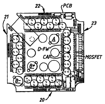
Fig. 2 is a general view of the PCB showing the arrangement of the components
thereon, the connection points for the components, and the positions of the
connectors
A, B+, and B-. The PCB is approximately in the form of a square. There are
twenty four mosfet/diode/capacitor circuits arranged in four sets of six, with
the four
sets occupying the four sides 20 to 23 of the square. The tourm
mosfet/diode/capacitor circuit down on the right-hand side of the square,
indicated as
MOSFET, CAP, and D-FW, is typical of the mosfet/diode/capacitor circuits. As -
shown, the diodes are located on the inside of the square, the capacitors
outside the _
CA 02311544 2000-OS-19
- WO 99/26806 PCT/GB98/03473
-6-
diodes, and the mosfets outside the capacitors. The mosfets each have three
terminals
and the capacitors each have two terminals. Each diode is shown as having
three
terminals, because each diode in fact consists of a pair of diode elements in
a single
casing; the circuitry on the PCB connects the two elements in parallel so that
they
effectively form a single diode.
The largest components are the capacitors. To minimize the size of the PCB,
the
mosfets are located substantially contiguous with each other along each side
of the
square, as are the diodes. On sides 20 to 22 of the square, the capacitors are
staggered in a zig-zag arrangement as shown to pack them into the same length
as the
diodes and mosfets. On side 23, the capacitors are in a straight line, and are
therefore
slightly offset from their associated diodes and mosfets. However, the spacing
between the diodes and the mosfets is the same on all four sides of the PCB,
for
reasons discussed later.
The three connectors A, B+, and B- are arranged along the lower left to upper
right
diagonal of the square, as shown, with the A and B+ connectors at opposite
corners
of the area inside the four sets of mosfet/diode/capacitor circuits and the B-
connector
at an outer corner. Figs. 3 and 4 show the track patterns on the two sides of
the
PCB. Fig. 3 shows the upper surface of the PCB; the A connector is connected
to
a solid area of track in the inside of the square. Fig. 4 shows the lower
surface of
the PCB (from the top, ie looking through the PCB); the B connector is
connected to
a solid area of track in the inside of the square and the B- connector is
connected to
the solid area of track on the outside of the square (and the B- connection
also uses
parts of some of the outside corners of the top surface of the PCB, as shown
in Fig.
3).
The areas of track for the A, B+, and B- connections form the buses shown in
Fig.
1A. The fact that these track areas are solid means that their current
carrying
capacity is high, and the tracks can be made of heavy copper of sufficient
thickness
(using conventional PCB ~ technology) to provide adequate capacity to carry
the
currents which the mosfet/diode/capacitor circuits have to carry. Thus the
present -
CA 02311544 2000-OS-19
_ gyp 9g/~gp6 PCT/GB98103473
_'7_
controller does not require conventional busbars. The control connections to
the
mosfets, and various auxiliary circuitry, are accommodated around the outer
edge of
the upper surface (Fig. 3) of the PCB.
Looking at Fig. 3, the central area of the inner square of track is solid
apart from
various holes which accommodate mounting bolts, the B+ connector, etc. This
central area extends outwardly across the four sets of six
mosfet/diode/capacitor
circuits in the form of four sets of six forgers separated by isolating lines;
three of the
fingers on the top side 22 are shown at 24 together with the two isolating
lines 25
separating those fingers. This division of the conductive area into distinct
forgers,
one for each mosfet/diode/capacitor circuit, effectively isolates the
mosfet/diode/capacitor circuits from each other, minimizing interactions
between
adjacent mosfet/diode/capacitor circuits. It will be noted that the isolating
lines are
shortened in the bottom corners of the inner square, to improve the current
flow
IS around the large holes in the inner tracking area in those corners.
The B+ tracking area in the inside of the square, shown in Fig. 4, has similar
forgers
separated by isolating lines, though these fingers do not need to extend as
far as the
fingers of the B- tracking area shown in Fig. 3. (The forgers are of
alternating
lengths along sides 20 to 22, matching the side-to-side staggering of the
capacitors on
those sides.) No separation of the A tracking area (around the outside of the
square
as shown in Fig. 4) for the different mosfet/diode%apacitor circuits is
required. If
desired, an additional B- connector may be provided at the opposite (top
right) corner
of the board, or three such additional connectors so that there is a B-
connector at each
corner of the board.
The generally square layout of the mosfet/diode/capacitor circuits (rather
than a linear
layout of a single line, or two parallel lines) results in good packing
density, short
current paths between the connectors and the mosfet/diode/capacitor circuits,
and
greater uniformity of the current paths to the different
mosfet/diode/capacitor circuits.
The placing of all the connectors on a common diagonal of the square, and the
placing
of the A and B+ connectors at opposite points along that diagonal, also
promotes
CA 02311544 2000-OS-19
- WO 99!26806 PCTlGB98/03473
_g_
greater uniformity of the current paths to the different
mosfet/diode/oapacitor circuits
and uniformity of heating of the different mosfet/diode/capacitor circuits. We
have
found that moving the terminals away from the positions shown progressively
degrades
the current sharing and increases differential heating.
In principle, the layout need not be a square; a hexagonal or circular layout
would
have similar properties. In fact, for equalization of the current paths
between the A
and B+ connectors, an elliptical layout with those connectors as foci would be
optimal.
However, a square layout has considerable other advantages.
The mosfets and, diodes carry high currents, and therefore need cooling. The
cooling
arrangement of the present controller is shown in Fig. 5, which is a section
through
the PCB in the region containing a single mosfet/diode/capacitor circuit. The
mosfet
and the diode are mounted on one side of the PCB, while the capacitor is
mounted on
the opposite side. This physical arrangement of the three elements of each
mosfet/diode/capacitor circuit also facilitates keeping the physical size, and
hence the
inductance, of the circuit small.
The mosfet and the diode are of similar size and shape, and each has a lug 30
extending downwardly from the end opposite the leads. A bar 31 of aluminium or
other heat-conducting material (seen in cross-section) is placed between
mosfet and
the diode. This bar has a hole (not shown) aligned with the lugs 30, and a nut
and
bolt 32 are placed through this hole and the lugs 30 and tightened to bring
the mosfet
and diode into good thermal contact with the bar 31. A plate 33 of aluminium
or
other heat-conducting material is bolted fixed to the bottom sides of the bars
31 to
form the final heat-dissipating element.
There are four sets of mosfet/diode%apacitor circuits, each containing six
circuits.
A separate bar 31 is used for each such set, with each bar being common to all
six
circuits in the set. The spacing between the mosfets and the diodes is the
same for
each set, so that the bars can be the same for all the sets. Since each nut
and bolt 32
engages with two components (the mosfet and the diode), located generally
CA 02311544 2000-OS-19
WO 99/26806 PCT/GB98/03473
-9-
symmetrically one on each side of the bar, the holes in the bar can be plain
untapped
drilled bores.
Obviously, this heat-dissipating construction can be used for a single set of
such
circuits, or even for a single such circuit, if the number of such circuits is
low.
Fig. 6 shows a second vehicle circuit, using an SEM (separately excited motor)
configuration. This circuit is broadly similar to the circuit of Fig. 1.
However,
instead of the armature being in series with the field coil and driven via a
bridge, the
armature and field coil are in parallel and the field coil F is excited via a
mosfet
bridge F-BR; also, there are separate shuts A-SH and F-SH for the armature and
field
coil, and a capacitor bank F-CAP for the field coil circuity. Further, the
bank of
mosfet/diode/capacitor switching circuits of Fig. 1 is replaced by a bank of
mosfet/diode/capacitor switching circuits, consisting of drive mosfets DR-
MOSFET,
braking mosfets B-MOSFET, and capacitors CAP. That is, the diodes of the Fig.
1
circuit are replaced by braking mosfets.
Each feature disclosed in this specification (which term includes the claims)
and/or
shown in the drawings may be incorporated in the invention independently of
other
disclosed and/or illustrated features.
The text of the abstract filed herewith is repeated here as part of the
specification.
A controller, for a battery-operated vehicle or the like, comprises a
plurality of
mosfet/diode/capacitor circuits. A printed circuit board PCB has the
mosfet/diode/capacitor circuits arranged in four sets, one set along each side
of the
board, and with the inner areas of the board on both sides and the outer area
on at
least one side being substantially solid tracking areas forming the
connections to the
circuits. The connectors A, B+, B- to circuits are located substantially along
a
diagonal of the board, with the connectors A and B+ to the two sides of the
diodes
located at opposite comers of the inner areas of the board. The inner tracking
areas
are divided by isolating lines into separate fingers for the respective
circuits. -
CA 02311544 2000-OS-19
WO 99/26806 PCT/GB98/03473
-10-
The mosfet and diode of each circuit are mounted on one side of the board and
the
capacitor on the other, with a heat sink bar located between the mosfet and
diode with
the mosfet and diode clamped to it by a nut and bolt passing through lugs on
the
mosfet and diode each matching a hole in the bar.