Note: Descriptions are shown in the official language in which they were submitted.
CA 02311800 2000-OS-26
PROCESS FOR SURFACE-MOUNTING A MICROWAVE PACKAGE ON A
PRINTED CIRCUIT AND PACKAGE AND PRINTED CIRCUIT FOR THE
IMPLEMENTATION OF THE PROCESS
The present invention relates to a process for
surface-mounting a microwave package, which includes an
electronic chip, on a printed circuit and to a package
and a printed circuit which are designed for
implementing this process.
It is known practice to mount an electronic
chip directly on a receiving printed circuit; it is
also known practice to mount the chip on a miniature
printed circuit in order to form a microwave package
which is then surface-mounted on the receiving printed
circuit. In both cases, it is known practice to make
the connections to the receiving printed circuit by
wire connections and to cover the microwave chip or
package with a protective lid. However, the use of such
mounting techniques in high volume is expensive since,
for high operating frequencies, it requires, for making
the wire connections, when furnishing the receiving
printed circuit, the use of microelectronic equipment;
without such equipment, it is virtually impossible,
using these mounting techniques, to work at frequencies
above 12 GHz.
The object of the present invention is to avoid
this drawback.
This is achieved by mounting a miniature
printed circuit bearing the chip on a receiving printed
circuit, in which the active face of the miniature
printed circuit bearing the chip is soldered to the
receiving printed circuit and in which earth planes
distributed over the two printed circuits form a kind
of cage constituting a screen around the chip.
According to the invention, what is proposed is
a process for the mounting of a microwave package on a
printed circuit, characterized in that it consists in
using, for the package, a microwave package having two
parallel faces, a first face of which has an electronic
CA 02311800 2000-OS-26
- 2 -
chip, conductors connected to the chip and earth planes
inserted between the conductors, and a second face of
which consists of an earth plane connected to the earth
planes of the first face, in producing the printed
circuit in such a way that it has a first face with, in
a region dedicated to the package, conductors and
earth planes and a second face consisting of an earth
plane connected to the earth planes of the first face
of the printed circuit, the first two faces having, on
the one hand, their earth planes and, on the other
hand, their conductors which, in a predetermined
position of the package on the printed circuit, are in
one-to-one contact, in placing the package in the
predetermined position and in connecting the package to
the printed circuit by soldering the conductors and the
earth planes in one-to-one contact.
According to the invention, what is proposed is
a microwave package for the implementation of a process
for mounting a package on a printed circuit, this
microwave package including a miniature printed circuit
with first and second faces, the first face having an
electronic chip and conductors connected to the chip,
and the second face consisting of an earth plane,
characterized in that the first face includes earth
planes, in that these earth planes are inserted between
the conductors and in that the miniature printed
circuit includes connections between the earth planes
of the first face and the earth plane of the second
face.
According to the invention, what is proposed is
a printed circuit for receiving a microwave package,
for the implementation of a process for mounting a
package on a printed circuit, this receiving printed
circuit including first and second faces, the first
face including, in a receiving region, conductors and
the second face consisting of an earth plane,
characterized in that the first face includes earth
planes in the receiving region, in that these earth
CA 02311800 2000-OS-26
- 3 -
planes are inserted between the conductors and in that
the receiving printed circuit includes connections
between the earth planes of the first face and the
earth plane of the second face.
The present invention will be more clearly
understood and further features will appear from the
description below and from the figures relating
thereto, which illustrate:
- in Figures 1 and 2, the views of one of the
faces of two printed circuits; this is the face which
bears, among other elements, conductors, and the view
in Figure 2 is a partial view;
- in Figure 3, a sectional view of the printed
circuits of Figures 1 and 2, after they have been
joined together by soldering;
- in Figure 4, a perspective view of one
embodiment of one of the elements described using
Figure 3; and
- in Figures 5 to 7, views corresponding to the
views in Figures 1 to 3, respectively, but in an
embodiment which includes the element in Figure 4.
In the various figures, the corresponding
elements are denoted by the same reference symbols.
In the following and in the claims, when
reference is made to a printed circuit one of whose two
sides is entirely metallized, and this side will be
soldered to a metal support, it will be assumed that
the metal support forms part of the printed circuit and
constitutes the earth plane thereof.
Figure 1 shows a microwave package for an
electronic chip P; it consists of a miniature printed
circuit, of which Figure 1 shows a square face ABCD
with conducting tracks L1 to L4, earth planes M1 to M4,
which are inserted between the tracks, and the chip P
linked to four decoupling elements such as E. The chip
P lies approximately in the middle of the face ABCD;
wires bonded at their ends provide the connections
between the various elements in this package.
CA 02311800 2000-OS-26
- 4 -
Tracks L2, L4 are connected respectively to two
microwave contacts on the chip, while the tracks L1, L3
supply the chip with bias voltages. Each of the earth
planes Ml to M4 is drilled with holes, such as Ha, Hb;
in total, there are fourteen holes distributed near the
periphery of the square ABCD.
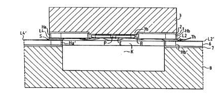
The package is illustrated in section in a
rectangle lying in the upper part of Figure 3; the
plane of section, along line XX, is perpendicular to
the plane of Figure 1 and is parallel to the tracks L2,
L4, lying along the middle of them. Figure 3 also
includes, adjoining the rectangle of the package, a
lower rectangle; this rectangle corresponds to a
sectional view of a printed circuit on which the face
ABCD of the package rests; the package is said to be
surface-mounted on the printed circuit.
The miniature printed circuit of the package
includes an insulating substrate 1 with, on one side,
the face illustrated in Figure 1 and, on the other
side, an earth plane comprising three successive
layers: a metal coating, a coating of solder 2 and a
conductive mechanical support 3 made, of brass; in order
to make the drawing easier to understand, the metal
coating on the substrate 1 and the solder, between this
coating and the mechanical support 3, have been merged
in the drawing in Figure 3 so as to show only a
conductive layer 2.
The package has the particular feature,
compared with a conventional package in which the
support 3 is a simple brass plate with parallel faces,
of possessing a projection or tab 3b in its support, on
the substrate side, level with a hole made in the
substrate for soldering the chip P to the earth plane.
Usually, that is to say without the tab 3b, the chip P
is soldered to the earth plane, directly on the support
3; its face opposite the earth plane is at a given
distance from that face of the miniature printed
circuit which bears the tracks L1 to L4. When, in order
CA 02311800 2000-OS-26
- 5 -
to protect the chip, resin is deposited thereon, it
proves impossible to have only the thin layer of resin
strictly needed for the protection; the resin, which
then greatly modifies the propagation medium on the
side with the chip connections, disturbs the operation
above frequencies greater than 10 GHz. The presence of
the tab 3b greatly reduces the said given distance;
that one of the faces of the miniature printed circuit
which bears the tracks L1 to L4 is then used as a
reference level for the amount of resin to be
deposited, thereby making it possible to control the
thickness of resin on the chip.
Figure 3 shows, in dotted lines, the holes Ha,
Hb referred to in the description of Figure 1; these
are, as in the case of the other twelve holes drilled
in the earth planes M1 to M4, holes with metallized
walls, or plated through-holes, which constitute
parallel conducting columns between the earth plane 2,
3 and the earth planes Ml to M4.
Figure 2 is a partial view of a receiving
printed circuit, in its part dedicated to the package
that has just been described above with the aid of
Figure 1, and of the rectangle in the upper part of
Figure 3. The rectangle in the lower part of Figure 3
corresponds to a sectional view of the printed circuit
of Figure l, in a plane of section along line XX; the
plane of section is perpendicular to the plane of
Figure 2. It should be noted that it is intentional
that the lines of section bear the same reference
symbols in Figures 1 and 2; this is so as to indicate
the fact that, when the package is mounted in the
predetermined position that it has to occupy on the
printed circuit, the two planes of section are
coincident.
The printed circuit in Figure 2 and in the
lower part of Figure 3 includes an insulating substrate
6 with, on one side, conducting tracks L1' to L4' and
earth planes M1' to M4', illustrated in Figure 2, and,
CA 02311800 2000-OS-26
- 6 -
on the other side, an earth plane comprising three
successive layers: a metal coating, a solder coating 7
and a mechanical brass support 8; here again, for the
ease of understanding the drawing, the metal coating on
the substrate 6 and the solder between this coating and
the mechanical support 8 have been merged in the
drawing in Figure 3.
The tracks L2', L4' are microwave tracks
through which the plane of section passes
longitudinally through their middle and the tracks L1',
L3' are tracks intended for supplying bias voltages.
Each of the earth planes M1' to M4' is drilled
with holes such as Ha', Hb'. These holes, the wall of
which is metallized, provide a conducting connection
between the earth planes M1' to M4' lying on one side
of the printed circuit and the earth plane 7, 8 lying
on the other side of the printed circuit.
In Figure 2, four points A', B', C', D' forming
the apexes of a square have been indicated by arrows;
they correspond to the exact positions that the apexes
ABCD of the face of the miniature printed circuit
illustrated in Figure 1 must occupy, respectively, when
th.e package is being mounted on the receiving printed
circuit; it is in this position of the package with
respect to its receiving printed circuit that the
section in Figure 3 is made. It should be pointed out,
by comparing Figures 1 and 2, that the earth planes and
the orifices of the plated through-holes lying in the
square A'B'C'D' correspond, point for point, in a
symmetry with respect to a plane, to the earth planes
and to the orifices of the plated through-holes lying
in the square ABCD; in the case of the conducting
tracks, this symmetry also exists, but only with
respect to part of the tracks of the square ABCD, since
the tracks extend less inside the square A'B'C'D' than
inside the square ABCD. Thus, when the apexes ABCD of
the miniature printed circuit are above the points
A'B'C'D' respectively, the conducting tracks L1' to L4'
CA 02311800 2000-OS-26
and the earth planes M1' to M4' are entirely opposite
the tracks and the corresponding earth planes of the
package; in addition, the fourteen plated through-holes
in the package lie along the extension of the fourteen
plated through-holes in the receiving printed circuit.
Connecting the package to its receiving circuit
consists, in the example described, in firstly applying
a thin layer of solder to the tracks and to the earth
planes which lie opposite when the square ABCD is above
the square A'B'C'D'; the package is then positioned on
the receiving circuit in such a way that the square
ABCD is exactly above the square A' B' C' D' and that the
facing tracks and the facing earth planes can be
soldered together by thermal bonding. In Figure 3, the
heat influx providing the thermal bonding has been
shown symbolically by an arrow Th; as regards the
solder layer which connects the tracks L4 and L4' after
thermal bonding, this has been denoted by S in
Figure 3.
The package, thus mounted on the receiving
printed circuit, has its chip, which is contained in a
kind of cage forming a screen, bounded upwardly by the
earth plane 2, 3, downwardly by the earth plane 7, 8
and laterally by the fourteen pairs of plated through-
holes in the package (the term "pair of plated through-
holes" should be understood to mean the holes, such as
Ha and Ha', which lie along the extension of each other
when the package is being mounted on its receiving
printed circuit), as well as the thickness of solder
between the holes, such as Ha and Ha'.
Figures 2 and 3 show that recessed into the
receiving printed circuit is a cavity K, of oval cross
section, which opens below the chip P when the package
is mounted on the receiving printed circuit. The
dimensions of this cavity are such that the distance
from the chip P to the closest walls of the earth plane
- 7, 8 is about five times greater than in the same
mounting but without the cavity; the function of this
' ~ CA 02311800 2000-OS-26
cavity is to prevent perturbations in the operation of
the chip which are due to the radiation being much too
close to a metal plane, in this case the earth plane
7, 8.
As a variant of the example described above,
the chip P may be mounted in a conventional manner,
that is to say on an earth plane such as 2, 3 without
the tab such as 3b; the chip may also not be protected
by a resin coating, given that, after the package has
been mounted on its receiving printed circuit, the chip
lies in a virtually closed space, the impermeability of
which may moreover be improved by a seal made of an
insulating material, for example a cement, placed all
around the package at the junction between the package
and the receiving printed circuit; taking into account
the expected performance, it is even possible, in some
cases, not to provide a cavity, vertically in line with
the chip, in the receiving printed circuit.
In addition, the package may be produced with
the chip placed on the miniature printed circuit in a
mounting called a bumped-chip or flip-chip mounting;
however, this mounting, in which the bumps on the chip
are in direct contact with the miniature printed
circuit, does not allow good heat dissipation since the
chip is no longer pressed against an earth plane which
serves as a heat sink for it.
Another variant of the examples described above
consists, in order to enclose in a kind of Faraday
cage, in replacing, in the miniature circuit, the
plated through-holes with metallizations produced on
the edge of the miniature printed circuit, between the
outer edges of the earth planes such as Ml to M4 and
the earth plane such as 2, 3.
An advantageous variant of the embodiment of
the microwave package and the receiving printed circuit
according to Figures 1 to 3 is described below with the
aid of Figures 4 to 7.
' CA 02311800 2000-OS-26
- 9 -
The tab 3b on the brass mechanical support 3
was, in the embodiment in Figures 1 and 3, obtained by
machining, an operation which is relatively expensive
in the case of mass production. In order to reduce the
cost, the idea has been to substitute the technique of
drawing for that of machining in the case of mass
production of the support 3. Since the support 3 is
small in size, 5 x 5 mm in the example described in the
case of the square ABCD in Figure 1, the cost of the
material used is negligible compared with the
manufacturing cost; the saving made by drawing allows
the manufacturing cost of this support to be reduced by
a factor of ten.
Added to this idea of producing the tab 3b by
drawing is the idea of modifying the microwave package
in such a way that the four earth planes M1 to M4 of
the miniature printed circuit, as they appear in
Figure 1, are replaced with earth planes formed by the
upper face of suitably placed tabs on the support; this
idea of earth planes obtained by tabs was therefore
extended to the idea of producing these tabs during the
same drawing operation as that for the tab 3b.
Unfortunately, it turned out that, in the case of the
package to be produced, the size of the tabs was too
great not to result, during the drawing operation, in
undesirable distortions of the brass block. In order to
avoid this drawback, it was decided to produce only
part of the planes M1 to M4 using tabs. This has led to
obtaining only about one third of the earth planes M1,
M3 using tabs and in choosing, for this third, tabs
which are perpendicular to the tracks L2, L4 of the
microwave contacts; this choice was guided by two
observations, namely that the screens produced by tabs
between earth planes prove to be more effective than
those produced by plated through-holes between earth
planes, and that the screens perpendicular to the
tracks are of greater importance than those parallel to
these tracks.
CA 02311800 2000-OS-26
- 10 -
Figure 4 is a perspective view of a support 3
obtained by drawing, as indicated above. In this view,
five tabs may be seen, namely the tab 3b and four tabs
Mla to M4a.
Figure 5 is a view which corresponds to the
view in Figure 1, but in an embodiment using the
support 3 in Figure 4. This view is distinguished from
that in Figure 1 by the fact that the earth planes M1
to M4 consist partly of the upper faces of the tabs Mla
to M4a, which upper faces are left uncovered by the
substrate of the miniature printed circuit and are
flush with the front face of the miniature printed
circuit. In order to distinguish the upper faces of the
tabs from the miniature printed circuit, they have been
shaded in Figure 5.
It should be noted that, everywhere the
miniature printed circuit is close to the tabs Mla to
M4a, it bears, on its edge and on its front face,
copper coatings; this makes it possible, when mounting
the miniature printed circuit on its brass mechanical
support 3, for there to be good wicking of the solder
between the tabs and the miniature printed circuit.
It should also be noted that their position
around the miniature printed circuit facilitates
"support/miniature printed circuit" mounting; this is
because the tabs serve as guiding elements for
positioning the miniature printed circuit on its
support.
The earth planes M1 to M4 in Figure 1 are
replaced in Figure 5 with the earth planes Mla + Mlb,
M2a, M3a + M3b, M4a, respectively. In these new earth
planes, the parts Mlb, M3b are copper coatings borne by
the front face of the miniature printed circuit and are
connected, via plated through-holes, to the earth plane
of the rear face of the miniature printed circuit.
The receiving printed circuit in Figures 2
and 3 may be used as the receiving circuit dedicated to
the microwave package described with the aid of
CA 02311800 2000-OS-26
- 11 -
Figures 4 and 5. As a variant, a receiving printed
circuit is proposed whose front face is illustrated, in
a partial view, in Figure 6. This is a receiving
circuit which is distinguished from that in Figures 2
and 3 only by the way in which its earth planes of the
front face are formed.
Whereas the earth planes M1' to M4' were all
obtained by metal coatings, in the variant in Figure 6
they consist partly of the upper faces of tabs; these
tabs are obtained by drawing a brass plate and the
mechanical support thus produced fulfils the same
function as the mechanical support 8 in Figure 3. These
tabs, referenced M1'a to M4'a, are placed so as to
correspond to the tabs Mla to M4a; they thus give, with
copper coatings M1'b to M3'b borne by the front face of
the receiving circuit, earth planes M1'a + Ml'b, M2'a,
M3'a + M3'b, M4'a which are equivalent to the earth
planes Ml to M4 in Figure 2, respectively.
The package in Figures 4 and 5 is connected to
its receiving circuit in Figure 6 as in the embodiment
described with the aid of Figures 1 to 3. Figure 7 is a
sectional view of the assembly thus produced. The line
of the plane of section is denoted YY in Figures 5
and 6; compared with the section in Figure 3, the plane
of section has been shifted so as to pass through the
tabs Mla, M2a, M1' a, M2' a.
In the sectional view in Figure 7, the supports
have been denoted by 3 and 8 in order to indicate that,
despite their tabs such as Mla and M2a and M1'a and
M2'a, they were equivalent to the supports 3 and 8
illustrated in Figure 3.
It should be noted that, in the embodiment in
Figures 4 to 7, the tabs Mla - M4a, M1'a - M4'a fulfil
two functions: (1) an earth plane by their upper faces
and (2) a connection between, on the one hand, the two
faces of the miniature printed circuit and, on the
other hand, the two faces of the receiving printed
circuit.
CA 02311800 2000-OS-26
- 12 -
In all or some of Figures 5 to 7, elements
appear which bear the same reference symbols 1, 2, 6,
7, K, P, etc. as elements already described with the
aid of Figures 1 to 3. These are elements equivalent to
those in Figures 1 to 3, so that the comments made with
regard to the description of Figures 1 to 3, for
example relating to the cavity K, remain valid within
the context of Figures 5 to 7.