Note: Descriptions are shown in the official language in which they were submitted.
CA 02311821 2000-OS-23
WO OO1Z5421 PC'C/F199/00883
1
METHOD AND ARRANGEMENT FOR CORRECTING PHASE ERROR IN
LINEARIZATION LOOP OF POWER AMPLIFIER
BACKGROUND OF THE INVENTION
The invention relates to amplifiers and in particular to a method and
arrangement for linearizing power amplifiers.
Linearized amplifiers are needed, for instance, for modern digital
wireless communication systems, because of the requirement that the spec-
trum of a signal to be transmitted must not spread outside the actual useful
band. Spreading of the spectrum results from non-linearity of amplifiers and
it
causes interference to adjacent channels, for instance. The linearity of ampli-
fying stages depends on how they are biased and they can be classified ac-
cording to linearity: a class A amplifier is the most linear but its
efficiency is
poor, whereas a class C amplifier's efficiency is good but it is at the same
time
highly non-linear. Good efficiency is an important property in power
amplifiers,
and this is particularly emphasized in wireless communication devices whose
battery capacity is limited. Therefore, amplifiers that have good efficiency
but
are non-linear and need to be linearized are used.
One known method of linearizing a non-linear radio-frequency
power amplifier is Cartesian feedback. In broad outline, its operational
princi-
ple is as follows: data to be transmitted is included in baseband signals I
and
Q. These signals are applied to an I/Q modulator, in which the signals are
combined and modulated directly to a final frequency. The final-frequency sig-
nal is amplified by one or more non-linear radio-frequency power amplifiers
and passed to an antenna. The amplified radio-frequency signal is sampled
after the last amplifying stage by a directional coupler, for instance. The
sam-
ple signal is applied to the I/Q modulator, in which it is demodulated to the
baseband, and the I and Q signals are separated therefrom. The baseband I
and Q sample signals are finally summed to the actual I and Q signals. This
causes predistortion in the I and Q signals, thanks to which the non-linearity
produced in the power amplifiers is at least partly cancelled.
In the above-described arrangement, both the IIQ modulator and
the I/Q demodulator receive a local oscillator signal from the same source. On
the other hand, the power amplifiers cause delay and the sampled I and Q
signals return in a wrong phase. This distortion can be compensated by ad-
justing the phase of the local oscillator signal applied to the I/Q modulator
or
CA 02311821 2000-OS-23
WO 00/25421 PCT/FI99/00883
2
I/Q demodulator considering the delay produced in the power amplifiers. In
order that the phase error could be corrected, its magnitude has to be meas-
ured first. EP 0 706 259 A1 discloses one method of measuring and correcting
a phase error in a Cartesian feedback loop. According to the method, the loop
is broken for the duration of measuring and the measuring is performed by
feeding excitation signals to the I and Q inputs of the loop and by measuring
the resultant signals at the outputs of the I/Q demodulator, and further, by
cal-
culating a phase error from the measurement results. The method has a
drawback that the loop has to be broken for the duration of the measuring, and
consequently switches are required for both feedback branches. Further, the
transmitter has to be turned off when operating the switches, in order for the
transmission spectrum not to spread. Moreover, amplification of an open loop
is typically much higher, than amplification of a corresponding closed loop,
whereby the effect of DC offsets of baseband operational amplifiers and noise
on the accuracy achieved with phase measuring is rather high. Amplification of
the open loop also varies much more than amplification of the closed loop, and
consequently it is difficult to carry out phase measuring at a given power
level.
US patent publication 5,175,879 discloses phase adjustment of a loop on a
continuous basis the loop being in a normal closed state. The method employs
a phase detector between the input of a linearization loop and the output of
an
I/Q demodulator. From the output of the phase detector, a phase difference
signal is further generated by means of an integrator for a phase shifter
which
corrects the phase. One drawback of the method is, for instance, that while
turning the amplifier on, the linearization loop may fitter and cause spectrum
spreading. Discontinuities of the phase shifter would also cause problems to
the implementation.
BRIEF DESCRIPTION OF THE INVENTION
The object of the invention is thus to provide a method to the effect
that the above-described problems can be solved. This is achieved by a
method for correcting a phase error in a linearization loop of a power
amplifier,
the loop comprising an 1/Q modulator, one or more delay-causing power am-
plifiers to be linearized, an I/Q demodulator for producing I and Q feedback
signals from the amplifier output signal, difference means of the I and Q
branches for producing I and Q difference signals from the I and Q feedback
signals and the 1 and Q input signals, the I/Q modulator and the I/Q demodu-
CA 02311821 2000-OS-23
WO 00/25421 PCT/F199/00883
3
lator receiving an oscillator frequency from the same local oscillator, and a
phase shifter, the method comprising determination of a phase error resulting
from delay produced in the linearization loop, which determination comprises
feeding excitation signals to the I and Q inputs of the linearization loop,
meas-
uring the signals resulting from the excitation signals and calculating the
phase
error by means of the measured signals and excitation signals, and correcting
the phase error by adjusting a phase of a local oscillator signal passing to
the
I/Q modulator or I/Q demodulator by means of the phase shifter, whereby the
method is characterized in that when determining the phase error, the signals
resulting from the excitation signals are measured from the I and Q difference
signals or from the I and Q input signals of the I/Q modulator and that the
phase error determination is performed the linearization loop being closed.
The invention is based on the idea that when using DC excitation
signals the phase error can be readily calculated from the I and Q baseband
signals of the linearization loop. A deviation of the measured resultant
vector
angle from the input vector angle indicates directly the phase error. By per-
forming the measuring with a plurality of I and Q input signal combinations,
the
phase errors of the branches can be averaged. When the excitation signals
are applied to the I and Q inputs of the linearization loop and the I and Q
dif-
ference signals or IIQ modulator input signals are used as measuring signals,
the phase error can be measured and compensated the linearization loop be-
ing closed.
The method of the invention has an advantage that the phase of the
linearization loop can be adjusted in a normal mode on an accurately defined
power level the loop being closed. The event of measuring and adjusting will
not make the spectrum spread harmfully to adjacent channels. At the modu-
lator input, signal levels are typically high, whereby interference signals do
not
cause considerable errors in measuring.
The invention also relates to a linearization arrangement of a power
amplifier, the arrangement comprising difference means, which form I and Q
difference signals out of the actual I and Q input signals and I and Q
feedback
signals of the linearization loop, a~ IlQ modulator, in which the data
containing, baseband I and Q difference signals received from the difference
means are combined and modulated to a final frequency, one or more delay
causing power amplifiers to be linearized by which the final-frequency signal
is
amplified whereafter it is applied to an antenna to be transmitted, a sampling
CA 02311821 2000-OS-23
WO 00/25421 PCTIF199/00883
4
arrangement, by which a sample signal is taken from the amplified final-
frequency signal prior to the antenna, an I/Q demodulator, to which said sam-
ple signal is applied and in which the sample signal is demodulated to the
baseband and the ! and Q sample signals which form said I and Q feedback
signals are separated therefrom, a local oscillator, from which a local
oscillator
signal is applied to the I/Q modulator and I/Q demodulator and a phase
shifter,
by which the phase of the local oscillator signal passing to the 1IQ modulator
or
lIQ demodulator is shifted for compensating the phase error of the
linearization
loop, the arrangement being arranged to determine the phase error by appiy-
ing DC excitation signals to the I and Q inputs of the difference means of the
linearization loop and by measuring the resultant signals, and to calculate
the
phase error resulting from the delay in the linearization loop by means of the
measured signals and the excitation signals, and to correct the determined
phase error, whereby the linearization arrangement is characterized by being
arranged to measure the signals resulting from the excitation signals from the
I
and Q difference signals or the I and Q input signals of the l/Q modulator
when
determining the phase error, and by being arranged to determine the phase
error while the linearization loop is closed.
By means of a linearization arrangement like this, the method of the
invention can be implemented by simple circuitries.
BRIEF DESCRIPTION OF THE DRAWINGS
In the following, the invention will be described in greater detail in
connection with preferred embodiments with reference to the attached draw-
ings, in which
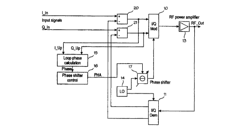
Figure 1 is a block diagram of a linearization arrangement of a
transmitter power amplifier in accordance with one embodiment of the inven-
tion,
Figure 2 illustrates operating states of a phase shifter in accordance
with one embodiment of the invention,
Figure 3 illustrates phase error determination in accordance with
one embodiment of the invention,
Figure 4 illustrates a change of phase caused by a phase shifter as
a function of a control value in accordance with one embodiment of the inven-
tion,
CA 02311821 2000-OS-23
WO 00/25421 PCT/FI99/00883
Figure 5 is a flow chart of a phase adjustment process in accor-
dance with one embodiment of the invention.
DETAILED DESCRIPTION OF THE INVENTION
A linearization arrangement of a transmitter power amplifier in ac-
s cordance with Figure 1 comprises, in broad outline, an I/Q modulator 10, an
I/Q demodulator 11, at least one power amplifier 13 to be linearized, a local
oscillator 14, a loop phase calculation unit 15, a phase shifter control unit
16
and a phase shifter 17. The I/Q modulator 10 and the I/Q demodulator 11 op-
erate on a quadrature modulation principle. It enables two separate signals to
be combined in a transmitter and to be transmitted on the same transmission
band and to be separated again from one another in a receiver. The principle
of the quadrature modulation is that two separate signais, i and Q (Inphase
and Quadrature phase), are modulated using the same carrier frequency, but
the phases of the carriers deviate from one another in such a manner that the
carrier of the signal Q lags 90° behind the carrier of the signal I.
After modula-
tion, the signals are summed. Thanks to the phase difference, the signals I
and Q can be separated from one another when demodulating the sum signal.
For the method to function, the local oscillator signals used by the modulator
and the demodulator, on the basis of which signals the carrier is formed, must
be mutually of the same frequency and in a correct phase.
The baseband I and Q signals containing data are applied to the I/Q
modulator 10, in which they are combined and modulated to a final frequency
(transmission frequency). The final-frequency signal is forwarded to a non-
linear power amplifier 13, in which the signal is amplified. There can be a
plu-
rality of power amplifier units 13 coupled in series. After amplification, the
sig-
nal RF_OUT is conveyed to an antenna (not shown) to be transmitted.
The amplified, final-frequency signal is sampled after the power
amplifier 13 and applied to the I/Q demodulator 11, in which the sample signal
is demodulated to the baseband and the I and Q sample signals are separated
therefrom. The obtained baseband I and Q sample signals are summed to the
actual I and Q signals by feeding them to summing means 20 and 21 through
inverting inputs. The means 20 and 21 can thus be difference amplifiers, for
instance. This predistorts the signals passing to the I/Q modulator 10 and fur-
ther to the power amplifier 13 such that the non-linearity caused by the power
amplifier 13 is cancelled to be as low as possible.
CA 02311821 2000-OS-23
wo oonsazi rcT~imooas~
6
The local oscillator unit 14 generates an oscillator signal that is ap-
plied to the I/Q demodulator 11 and via the phase shifter 17 to the I/Q modu-
lator 10. The phase of the local oscillator signal coming to the I/Q modulator
is adjusted in the phase shifter 17, since the sample signal applied to the
5 I/Q demodulator 11 and modulated in the I/Q modulator 10 is delayed in the
power amplifier 13. In order for the sample signal to be correctly
demodulated,
the local oscillator signal and the sample signal to be applied to the I/Q de-
modulator must be in a correct phase with respect to each other. The delay
caused to the signal in the power amplifier is thus compensated by the phase
10 shifter 17. Alternatively, the phase shifter can be located in a signal
branch
leading from the local oscillator 14 to the I/Q demodulator 11.
Figure 5 illustrates a phase adjustment process of a preferred em-
bodiment of the invention for one frequency. For tuning the phase parameters
of the entire transmitter frequency band, the process is performed on one or
more occasions at one or more frequencies, depending on the implementation
of the phase shifter. The parameters tuned at different frequencies are stored
in the memory of the device.
The blocks of the flow chart operate as follows:
1} It is tested whether the transmitter is stable 51.
First the transmitter is switched on. To ensure stability, the value of
an oscillation detector (not shown) is checked and the signals I UP and Q_UP
are measured. The oscillation detector is based on detecting high-frequency
interference signals which appear in the baseband I and Q signals of the line-
arization loop in the course of oscillation. If the amplitude of a high-
frequency
interference signal exceeds a given limit value, a conclusion can be made that
the transmitter is unstable. In addition, the measured I UP and Q UP signals
are compared with the preset limit value. If one or both of the signals exceed
the limit value, the phase error of the linearization loop is about
180°, i.e. the
transmitter is unstable. If the transmitter is found unstable, a new, better
initial
value has to be searched 52 for the phase shifter prior to phase measuring. If
the transmitter is stable, a direct transfer to step 3) is performed 53.
2) A stable operating state is searched 52.
A stable operating state is searched by using the original phase
shifter 17 control value, indicated by point 0 in Figure 2, as the initial
value. In
Figure 2, the mutual distance between points 0 to 9 representing the operating
state of the phase shifter 17 corresponds to a change M in the control value
of
CA 02311821 2000-OS-23
WO 00/25421 PCT/F199/00883
7
the phase shifter 17. First the control value is increased by a predetermined
amount M, whereby a transfer is performed to point 1 in Figure 2 and stability
is checked in the same manner as in step 1) 51. If stability is not achieved,
the
original control value is decreased by M, i.e. a transfer is performed to
point 2
in Figure 2. If stability is not achieved by this either, the original control
value
will be increased next by 2 x M, i.e to point 3. Next, the original control
value is
decreased by 2 x M, i.e. to point 4. This procedure will be repeated until a
sta-
ble state is found. If a stable state is not found within the whole range of
360°,
a fault report will be given and the transmitter is prevented from being
started.
Trial points can be any other number than the ten points used in this example.
3) A reference excitation is fed and the signals I_UP and Q UP are
measured 53.
A reference excitation is fed to the linearization loop: I_IN = 0 V,
Q_IN = 0 V and the corresponding signals I UP and Q UP (I~e, = I_UP, Q~er =
Q UP) are measured. This is necessary to have a correct reference point for
the signals to serve as a zero-point in calculation. At this stage the
transmitter
can be turned off (the linearization loop is broken) or on (the loop is
closed).
This step is not necessary. The step facilitates implementation of the device
and enables better accuracy of phases. The step can be performed only in
specific less frequently repeated periods than the actual phase adjustment
process, for instance.
4) The actual excitation is fed to the linearization loop and the sig-
nals I UP and Q UP are measured 54.
The actual excitation (I_IN = I;~, Q_IN = Q,~) is fed to the linearization
loop and the signals I_UP and Q_UP (Imeag = 1 UP, Qm~g = Q_UP) are meas
ured. The excitation is typically located on IQ plane on the axes (I IN = Vdc,
Q_IN = 0 or I_IN = 0, Q_IN = Vdc or I IN = -Vdc, Q_IN = 0 or I,IN = 0, Q_IN =
-Vdc), but it can also be located anywhere else on IQ level. The value of the
excitation signal typically corresponds to the RMS value of the I and Q
signals
of a normal modulated transmission. A higher or lower level signal can also be
used. The power level set by transmitter power control can be any level, but
the highest stability is achieved if the 'transmitter has the same power
during
the measuring as in the normal operation.
5) The phase error is calculated and the control value of the phase
shifter 17 is corrected accordingly 55.
CA 02311821 2000-OS-23
WO 00/Z5421 PCT/F199/00883
8
The phase error is calculated from the measured signals by follow-
ing equations:
The phase angle a of the actual excitation signals I;~ and Q;~ (Figure
3, point A):
a = arctan Q'" , when l;" > 0 (1.1 )
I in
a =180° + arctan Q'" , when l;" < 0 (1.2)
I;,.
If 1;~ = 0 and Q;" > 0, then a = 90° and
if I;" = 0 and Q;n < 0, then a = 270°.
The phase angle ~i of the signals Imeas and Qmeas measured in step 4)
54 (Figure 3, point B) is given by:
~raens - ~rrJ
~3 = arctan m x , when (Imeas - Let) > 0 (2.1 )
Irne".~ - I~er
Qmeur QreJ
~3=180°+arctan m x , when (Imeas - Iret) ~ ~ (2.2)
I merrx I rcJ
If (Imeas - Iret) = 0 and (Qmeas - Q.et) ' 0, then ~3 = 90° and
If (Imeas - Iret) _ ~ and (Qmeas - Qret) < ~~ then ,l3 = 270°
where
m = 1, when imbalance of IQ amplitude is not considered and
l,ef and Q~er = the reference points of measuring in accordance with
step 3) 53 (Figure 3, point C). If the Irer and Q~~ values are not determined,
they
are deleted from the formulae (2.1) and (2.2), or alternatively, they are
given
the value zero.
The phase error a is given by:
A=(3-a (3.1)
CA 02311821 2000-OS-23
WO 00/25421 PCT/F199/00883
9
CONSIDERATION OF IQ AMPLITUDE IMBALANCE
Consideration of the amplitude imbalance may be necessary, if any
other vector than one in the direction of the axis I or Q is selected to act
as an
excitation signal. Consideration is effected as follows:
Step 1:
Excitation signal I IN = Vpc, and Q_IN = 0
A phase is searched, the measuring signals being I UP = the
maximum and Q UP = the minimum
I UP amplitude is measured, I UP = N
Step 2:
Excitation signal I_IN = 0 and Q IN = Vpc,
A phase is searched, the measuring signals being I_UP = the mini-
mum and Q UP = the maximum
Q UP amplitude is measured, Q UP = P
Step 3:
A correction factor m is calculated
_N
m=
P
which is used for calculating the phase angle ~3 of the signal to be
measured in accordance with the formulae (2.1 ) and (2.2).
The phase error being determined, the control value of the phase
shifter 17 is corrected for the magnitude of the phase error by the following
equation:
PHA, = PHAo - ~ ,
where PHA, is the new control value of the phase shifter 17, PHAo
is the old control value in store, 8 is the phase error and K is the average
slope
of the phase shifter 17, whereby K = ylx in accordance with Figure 4. The
phase range determined by a variable y depends on the shape of the phase
adjustment curve and where the 360 ° point is located on the curve so
that the
determined, average slope K would depict the phase adjustment curve of the
phase shifter 17 as well as possible. The case shown in Figure 4 is intended
to
illustrate the average slope K by way of example only. In Figure 4, the axis A
represents a phase shift caused by the phase shifter 17 and the axis PHA rep-
resents the control value of the phase shifter 17.
CA 02311821 2000-OS-23
WO 00/25421 PCT/FI99/00883
6) Stability of the transmitter is tested 56 as in step 1 ) 51 by means
of the new control value of the phase shifter 17. If the transmitter
oscillates, i.e.
it is not stable, a return to step 2) 52 to the beginning of the phase
adjustment
process is performed. If a stable state is not achieved with the following
round,
5 a fault report is given and the transmitter is prevented from being started.
7) It is checked whether a discontinuity is passed on the phase
curve 57, when a transfer from the old value PHAo to a new value PHA, of the
phase shifter 17 is made. If yes, a return to step 3) 53 is performed and the
phase adjustment process is repeated. If the discontinuity is passed also next
10 time, a fault report is given and the transmitter is prevented from being
started.
Step.7) 57 makes it possible that the phase adjustment range of the
phase shifter 17 need not be highly accurate. If a phase shifter with
continuous
control is used alone, the adjustment range should in practice exceed
360°,
since in general the phase adjustment range of the phase shifter is not quite
accurate due to various non-ideal factors. For instance, at different frequen-
cies the same control value of the phase shifter may cause a different phase
shift. The adjustment range can be, for instance, 0 to 400°, when the
range
360 to 400° corresponds to the range 0 to 40°. tt is ensured
thereby that the
complete 360° will be covered. A discontinuity refers to a point at
which, like in
the example, a transfer is made from the value 400° back to the
starting value
0°. Also a change in the state of an optional step phase shifter can
produce a
discontinuity. When using a phase shifter with continuous control and step
phase shifters together, the adjustment range of the phase shifter with con-
tinuous control must exceed the largest phase shift caused by the change in
state of the step phase shifter in order that a continuous phase adjustment
range would be achieved. If a phase shifter with continuous control, not
having
a discontinuity, is used, this step is not necessary. It is not relevant to
the in-
vention, how the phase shifter is implemented.
8) Finally, the obtained phase shifter control value PHA, (not
shown) 58 is stored and it is utilized to control the phase shifter 17 at a
given
transmitter frequency range, until the phase adjustment process on said fre
quency range is repeated.
The phase adjustment process can be repeated (at a given fre
quency) several times by means of the same or different excitations, whereby
the new control value of the phase shifter 17 can be deduced (e.g. by suitably
averaging) from the provisional results obtained by different excitations.
CA 02311821 2000-OS-23
WO 00/25421 PCT/FI99/00883
11
There are several alternatives to implement the phase adjustment
process and use it. For instance, the above-described process can be em
ployed when initializing a transmitter (e.g. calibration for production),
repeated
at given intervals, when a transmitter parameter changes or on the initiative
of
an external excitation signal.
For instance, the available frequency band of 20 MHz can be di-
vided into 20 sub-bands, each of which is determined to have a separate con-
trol value of the phase shifter 17.
The operations of various steps (1 to 8) of the above-described
phase adjustment process can be performed between normal transmissions at
a suitable moment. The whole process can be distributed to a plurality of mo
ments, for instance, to various time slots of a TDMA transmission.
The present invention is intended for application to the TETRA
(Terrestrial Trunked Radio) system, but application of the method of the inven
tion to systems of any other type is by no means excluded. It is obvious to a
person skilled in the art that as technology advances the basic idea of the in-
vention can be implemented in a variety of ways. Thus the invention and its
embodiments ace not restricted to the above-described examples but they can
vary within the scope of the claims.