Note: Descriptions are shown in the official language in which they were submitted.
CA 02311842 2000-06-02
- 1 - CFO 14523 ~& C ~
METHOD OF MANUFACTURING A LIQUID
DISCHARGE HEAD, LIQUID DISCHARGE HEAD
MANUFACTURED BY THE SAME METHOD,
AND METHOD OF MANUFACTURING A MINUTE
MECHANICAL APPARATUS
BACKGROUND OF THE INVENTION
Field of the Invention
This invention relates to a liquid discharge head
for discharging desired liquid by the creation of a
bubble occurring by heat energy being caused to act on
the liquid, and a method of manufacturing such liquid
discharge head. Particularly the present invention
relates to a method of manufacturing a liquid
discharge head having a movable member displaced by
the utilization of the creation of a bubble, a liquid
discharge head manufactured by the same method, and a
method of manufacturing a minute mechanical apparatus.
Also, the present invention can be applied to
apparatuses such as a printer for effecting recording
on recording mediums such as paper, yarn, fiber,
cloth, metals, plastics, glass wood and ceramics, a
.copier, a facsimile apparatus having a communication
system and a word processor having a printer portion
and an industrial recording apparatus compositely
combined with various processing apparatuses.
The term "recording" in the present invention
CA 02311842 2000-06-02
- 2 -
means not only imparting meaningful images such as
characters and figures to the recording mediums, but
also imparting meaningless images such as patterns to
the recording mediums.
Related Background Art
Fig. 12 of the accompanying drawings is a partly
broken away perspective view showing a liquid
discharge head according to the prior art.
As shown in Fig. 12, the liquid discharge head
according to the prior art has a substrate 1004 on
which a plurality of heaters 1005 which are bubble
creating elements for giving head energy for creating
bubbles in liquid are provided in parallel, and a top
plate 1001 joined onto this substrate 1004.
The substrate 1004 comprises a base body of
silicon or the like on which silicon oxide film or
silicon nitride film are formed for the purposes of
insulation and heat accumulation, and electrical
resistance layers and wiring electrodes constituting
the heaters 1005 being patterned thereon. By a
voltage being applied from these wiring electrodes to
the electrical resistance layers to thereby flow an
electric current to the electrical resistance layers,
the heaters 1005 generate heat. On the substrate
1004, there are provided packaging electrodes 1003 to
which external terminals (not shown) for supplying an
electric current to the heaters 1005 are connected.
CA 02311842 2000-06-02
- 3 -
The top plate 1001 is for constituting a
plurality of liquid flow paths 1007 corresponding to
the heaters 1005 and a common liquid chamber 1010 for
supplying the liquid to the liquid flow paths 1007,
and is integrally provided with flow path side walls
1001a extending from the ceiling portion thereof to
among the heaters 1005. Also, the upper surface of
the top plate 1001 is provided with an ink supply
communication opening 1002 for causing the liquid
supplied from the outside to flow into the common
liquid chamber 1010. The top plate 1001 is formed of
a silicon material, and the pattern of the liquid from
paths 1007 and the common liquid chamber 1010 can be
formed by etching, and the portions of the liquid flow
paths 1007 can be etched and formed after a material
such as silicon nitride or silicon oxide which
provides the flow path side walls 1001a is accumulated
on the silicon substrate by a conventional film
forming method such as CVD.
A wall portion is provided on the fore end
surface of the top plate 1001, and this wall portion
is formed with a plurality of discharge openings 1006
corresponding to the respective liquid flow paths 1007
and communicating with the common liquid chamber 1010
through the liquid flow paths 1007.
Fig. 13 of the accompanying drawings is a partly
broken away perspective view showing another example
CA 02311842 2000-06-02
- 4 -
of the liquid discharge head according to the prior
art.
The liquid discharge head shown in Fig. 13 is
provided with cantilever-like movable members 2009
disposed in face-to-face relationship with heaters
2005. The movable members 2009 comprise thin film
formed of a silicon material such as silicon nitride
or silicon oxide or nickel or the like excellent in
elasticity. These movable members 2009 are disposed
at a predetermined distance from the heaters 2005 so
as to have fulcrums upstream of the heaters 2005 and
further have free ends downstream with respect to
these fulcrums.
The top plate 2001, the ink supply communication
opening 2002, the packaging electrodes 2003, the
substrate 2004, the heaters 2005, the discharge
openings 2006, the liquid flow paths 2007 and the
common liquid chamber 2013 of the liquid discharge
head are similar to those of the liquid discharge head
shown in Fig. 12 and therefore need not be described
in detail.
Figs. 14A to 14D of the accompanying drawings are
cross-sectional views along the direction of the flow
paths for illustrating the liquid discharging method
by the liquid discharge head shown in Fig. 13.
As shown in Fig. 14A, when the heater 2005 is
caused to generate heat, the heat acts on the ink
CA 02311842 2000-06-02
- 5 -
between the movable member 2009 and the heater 2005,
whereby a bubble 2008 based on a film boiling
phenomenon is created and grows on the heater 2005.
Pressure resulting from the growth of this bubble 2008
preferentially acts on the movable member 2009, which
is thus displaced so as to greatly open toward the
discharge opening 2006 side about the fulcrum, as
shown in Fig. 14B. By the displacement or displaced
state of the movable member 2009, the propagation of
the pressure based on the creation of the bubble 2008
or the growth of the bubble 2008 itself is directed to
the discharge opening 2006 side, and the liquid
(liquid droplet 2010) is discharged from the discharge
opening 2006, as shown in Fig. 14C.
As described above, the movable member 2009
having a fulcrum on the upstream side (the common
liquid chamber side) of the flow of the liquid in the
liquid flow path 2007 and having a free end on the
downstream side (the discharge opening 2006 side)
thereof is provided on each heater 2005, whereby the
direction of propagation of the pressure of the bubble
2008 is directed toward the downstream side and thus,
the pressure of the bubble 2008 directly and
efficiently contributes to discharge. The direction
of growth itself of the bubble 2008, like the
direction of propagation of the pressure of the
bubble, is directed toward the downstream side, and
CA 02311842 2000-06-02
- 6 -
the bubble grows larger on the downstream side than on
the upstream side. The direction of the growth itself
of the bubble 2008 is thus controlled by the movable
member 2009 to thereby control the direction of
propagation of the pressure of the bubble 2008,
whereby fundamental discharge characteristics such as
discharge efficiency and discharging force or
discharge speed can be improved.
On the other hand, as shown in Fig. 14D, when the
bubble 2008 enters its disappearing step, the bubble
2008 rapidly disappears by the combined effect with
the elastic force of the movable member 2009 itself,
and the movable member 2009 finally returns to its
initial position shown in Fig. 14A. At this time, in
order to make up for the contracted volume of the
bubble and to make up for the discharged volume of the
liquid, the liquid flows from the upstream side, i.e.,
the common liquid chamber side, and the refilling of
the liquid flow path 2007 with the liquid is effected,
and this refilling with the liquid is effected
efficiently and rationally with the returning action
of the movable member 2009.
In a method of manufacturing a liquid discharge
head according to the prior art shown in Fig. 15 of
the accompanying drawings, movable members 2009 are
first formed on a substrate 2004 on which heaters
2005, etc. are provided. The movable members 2009 are
CA 02311842 2000-06-02
_ 7 _
made by a series of semiconductor processes
comprising, for example, the formation of a sacrifice
layer aluminum pattern, the formation of SiN layers
forming the movable members 2009 and the patterning of
the SiN layers. As described above, devices such as
the movable members are provided on the surface of the
substrate 2004 and thus, the surface of the substrate
2004 has unevenness of a height of the order of
3 to 10 um.
Next, a nozzle wall member 2010 for constituting
liquid flow paths 2007 and a common liquid chamber
2013 (see Fig. 13 for both) between the substrate 2004
and a top plate 2001 is joined onto the substrate
2004. The upper surface of the nozzle wall member
2010 to which the top plate 2001 is to be joined is
then flattened.
Next, the top plate 2001 is joined to the upper
surface of the nozzle wall member 2010, and an orifice
plate 2011 formed with discharge openings 2006 is
joined to an end surface in which the liquid flow
paths 2007 open. By the above-described steps, the
liquid discharge head according to the prior art shown
in Fig. 13 is manufactured.
However, in the manufacturing method described
with reference to Fig. 15, it is necessary to
accurately join the nozzle wall member 2010 onto the
substrate 2004 and further, it is necessary to flatten
CA 02311842 2000-06-02
_ g _
the upper surface of the nozzle wall member 2010
before the joining of the top plate 2001 and
therefore, the manufacturing steps have been
cumbersome.
Also, when this wall member is to be formed of an
organic material, thick film of the above-mentioned
thickness can be formed if dry film is used, but the
surface of the substrate is uneven as described above
and therefore, not only it has been difficult to
achieve the flattening of the upper surface of the
wall member, but there has been the fear that the
movable members are deformed by the dry film.
Further, it has been difficult to form thick film of a
thickness of several tens of um, by the use of the
conventional wet process.
SUMMARY OF THE INVENTION
So, the present invention has as its object to
provide a liquid discharge head in which the upper
surface of a wall member can be flattened and the
manufacturing time for which can be shortened and
which is provided with a wall member formed into thick
film having a thickness of several tens of um, a
method of manufacturing the liquid discharge head, a
minute mechanical apparatus and a method of
manufacturing the minute mechanical apparatus.
To achieve the above object, the liquid discharge
CA 02311842 2000-06-02
_ g _
head of the present invention is a liquid discharge
head having a discharge opening for discharging liquid
droplets therefrom, a wall member constituting a
liquid flow path communicating with the discharge
opening to supply liquid to the discharge opening, a
substrate provided with a bubble creating element for
creating a bubble in the liquid filling the liquid
flow path, and a movable member supported by and fixed
to the substrate with the discharge opening side
thereof as a free end at a position on the substrate
which faces the bubble creating element with a gap
between it and the substrate, the free end of the
movable member being displaced in a direction opposite
to the substrate by pressure produced by creating the
bubble, and the pressure being directed to the
discharge opening side to thereby discharge the
droplet of the liquid from the discharge opening,
characterized in that the wall member is constructed
by providing and patterning liquid resin of a negative
type hardened when exposed to light on a surface on
which the movable member is formed.
According to the liquid discharge head
constructed as described above, as compared with a
case where an inorganic material such as SiN or Si0 is
formed into film to thereby form a wall member, it
becomes possible to shorten the manufacturing time.
Further, according to the present invention, the wall
CA 02311842 2000-06-02
- 10 -
member is formed by exposing a predetermined portion
of resin of the negative type applied onto the
substrate to light to thereby harden it and therefore,
unlike the conventional wet process, it becomes
possible to form thick film having a thickness of
several tens of pm.
Also, preferably the wall member may be of a
construction formed by a forming method having the
step of applying the liquid resin to that surface of
the substrate on which the movable member is provided
by spin coating, the step of exposing to light and
hardening that portion of the applied resin which
constitutes the wall member, and the step of removing
that portion of the applied resin which is not
hardened.
Further, the forming method has the step of
effecting the baking of the resin at a temperature
equal to or higher than the melting point of the
hardened resin after the step of removing that portion
of the applied resin which is not hardened, whereby
the levelling flow of the upper surface of the wall
member is effected highly accurately. Therefore, it
is not necessary to flatten the upper surface of the
wall member by polishing or the like which is a
post-step, and the manufacturing steps for the liquid
discharge head are simplified and further, it becomes
possible to manufacture the liquid discharge head
CA 02311842 2000-06-02
- 11 -
inexpensively.
Furthermore, by adopting a construction in which
the resin contains a solid component of 50 $ or more
and the average molecular weight thereof is 10,000 or
less, the viscosity of the resin becomes relatively
low and it becomes possible to flatten the resin well
at the applying step by spin coating and also, the
resin can be made to flow well into the gap between
the substrate and the movable member. Therefore, the
possibility of flexure or bending occurring to the
movable member when the resin is applied by spin
coating can be reduced.
Also, the method of manufacturing a liquid
discharge head of the present invention is a method of
manufacturing a liquid discharge head having a
discharge opening for discharging liquid droplets
therefrom, a wall member constituting a liquid flow
path communicating with the discharge opening to
supply liquid to the discharge opening, a substrate
provided with a bubble creating element for creating a
bubble in the liquid filling the liquid and flow path,
and a movable member supported by and fixed to the
substrate with the discharge opening side thereof as a
free end at a position on the substrate which faces
the bubble creating element with a gap between it and
the substrate, the free end of the movable member
being displaced in a direction opposite to the
CA 02311842 2000-06-02
- 12 -
substrate by pressure created by creating the bubble,
and the pressure being directed to the discharge
opening side to thereby discharge the droplet of the
liquid from the discharge opening, characterized by
the step of using resin of a negative type hardened
when exposed to light as a material forming the wall
member, and applying the liquid resin to that surface
of the substrate on which the movable member is
provided by spin coating, the step of exposing to
light and hardening that portion of the applied resin
which constitutes the wall member, and the steps of
removing that portion of the applied resin which is
not hardened.
Thereby, as compared with a case where an
inorganic material such as SiN or Si0 is formed into
film to thereby form a wall member, the manufacturing
time is shorted and further, unlike the conventional
wet process, it becomes possible to form thick film of
a thickness of several tens of um.
Further, there may be adopted a construction
having the step of effecting the baking of the resin
at a temperature equal to or higher than the fusing
point of the hardened resin after the step of removing
that portion of the applied resin which is not
hardened.
Furthermore, there may be adopted a construction
in which the resin contains a solid component of 50
CA 02311842 2000-06-02
- 13 -
or more and the average molecular weight thereof is
10,000 or less.
Also, the minute mechanical apparatus of the
present invention is a minute mechanical apparatus
having a first substrate on the surface of which a
wall member constituting a liquid flow path is
provided, a movable member supported by and fixed to
the first substrate with one end portion thereof as a
free end with a gap between it and the first substrate
in the liquid flow path on the first substrate, and a
second substrate joined to the upper surface of the
wall member, characterized in that the wall member is
constructed by liquid resin of a negative type
hardened when exposed to light being provided and
patterned on that surface of the first substrate on
which the movable member is formed.
Further, preferably the resin may contain a solid
component of 50 % or more and the average molecular
weight thereof may be 10,000 or less.
Also, the method of manufacturing a minute
mechanical apparatus of the present invention is a
method of manufacturing a minute mechanical apparatus
having a first substrate on the surface of which a
wall member constituting a liquid flow path is
provided, a movable member supported by and fixed to
the first substrate with one end portion thereof as a
free end with a gap between it and the first substrate
CA 02311842 2000-06-02
- 14 -
in the liquid flow path on the first substrate, and a
second substrate joined to the upper surface of the
wall member, characterized by the step of using resin
of a negative type hardened when exposed to light as a
material forming the wall member, and applying the
liquid resin to that surface of the substrate on which
the movable member is provided by spin coating, the
step of exposing to light and hardening that portion
of the applied resin which constitutes the wall
member, and the step of removing that portion of the
applied resin which is not hardened.
Preferably there may be adopted a construction
having the step of effecting the baking of the resin
at a temperature equal to or higher than the melting
point of the hardened resin after the step of removing
that portion of the applied resin which is not
hardened.
BRIEF DESCRIPTION OF THE DRAWINGS
Fig. 1 is a cross-sectional view along the
direction of a liquid flow path for illustrating the
structure of a liquid discharge head which is an
embodiment of the present invention.
Fig. 2 is a cross-sectional view of an element
substrate used in the liquid discharge head shown in
Fig. 1.
Fig. 3 is a typical cross-sectional view in which
CA 02311842 2000-06-02
- 15 -
the element substrate shown in Fig. 2 is sectioned so
as to cut the main elements of the element substrate
longitudinally.
Fig. 4 is a plan view of a liquid discharge head
unit carrying thereon the liquid discharge head shown
in Fig. 1.
Figs. 5A, 5B, 5C, 5D and 5E are views for
illustrating a method of forming a movable member on
the element substrate.
Fig. 6 is a view for illustrating a method of
forming SiN film on the element substrate by the use
of a plasma CVD apparatus.
Fig. 7 is a view for illustrating a method of
forming SiN film by the use of a dry etching
apparatus.
Figs. 8A, 8B, 8C and 8D are step cross-sectional
views for illustrating a method of forming movable
members and flow path side walls on the element
substrate.
Figs. 9A, 9B and 9C are perspective views for
illustrating the method of forming the movable members
and the flow path side walls on the element substrate.
Figs. l0A and lOB are views for illustrating the
side rinse step at the step of forming the flow path
side walls.
Fig. 11 shows the state after the spin coat step
and the side rinse step have been effected at the step
CA 02311842 2000-06-02
- 16 -
of forming the flow path side walls.
Fig. 12 is a partly broken away perspective view
showing a liquid discharge head according to the prior
art.
Fig. 13 is a partly broken away perspective view
showing another example of the liquid discharge head
according to the prior art.
Figs. 14A, 14B, 14C and 14D are cross-sectional
views along the direction of a flow path for
illustrating the liquid discharging method by the
liquid discharge head shown in Fig. 13.
Fig. 15 is a perspective view for illustrating a
method of manufacturing the prior-art liquid discharge
head shown in Fig. 13.
DESCRIPTION OF THE PREFERRED EMBODIMENTS
As an embodiment applicable to the present
invention, description will now be made of a liquid
discharge head having a plurality of discharge
openings for discharging liquid therefrom, a first
substrate and a second substrate joined to each other
to thereby constitute a plurality of liquid flow paths
communicating with the respective discharge openings,
a plurality of energy conversion elements disposed in
the respective liquid flow paths to convert electrical
energy into the discharge energy of the liquid in the
liquid flow paths, and a plurality of elements or
CA 02311842 2000-06-02
- 17 -
electric circuits differing in function from one
another for controlling the driving condition of the
energy conversion elements, the elements or the
electric circuits being allotted to the first
substrate and the second substrate in conformity with
the functions thereof.
Fig. 1 is a cross-sectional view along the
direction of the liquid flow paths of a liquid
discharge head which is an embodiment of the present
invention.
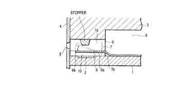
As shown in Fig, l, this liquid discharge head
has an element substrate 1 on which a plurality (only
one of which is shown in Fig. 1) of heat generating
members 2 for giving heat energy for creating a bubble
in liquid are provided in parallel, a top plate 3
joined onto this element substrate 1, an orifice plate
4 joined to the fore end surfaces of the element
substrate 1 and the top plate 3, and a movable member
6 installed in a liquid flow path 7 constituted by the
element substrate 1 and the top plate 3.
The element substrate 1 comprises a substrate of
silicon or the like and silicon oxide film or silicon
nitride film directed to insulation and heat
accumulation and formed thereon, and electrical
resistance layers and wiring constituting the heat
generating members 2 and patterned thereon.
A voltage is applied from this wiring to the
CA 02311842 2000-06-02
- 18 -
electrical resistance layers to thereby flow an
electric current to the electrical resistance layers,
whereby the heat generating members 2 generate heat.
The top plate 3 is for constructing a plurality
of liquid flow paths 7 corresponding to the respective
heat generating members 2 and a common liquid chamber
8 for supplying the liquid to the liquid flow paths 7
between it and the element substrate 1. Flow path
side walls 9 constituting the plurality of liquid flow
paths 7 and the common liquid chamber 8 on the element
substrate 1 are formed of photosensitive epoxy resin
of a negative type on the element substrate 1, as will
be described later with reference to Fig. 16 and Figs.
9A to 9C.
The orifice plate 4 is formed with a plurality of
discharge openings 5 corresponding to the liquid flow
paths 7 and communicating with the common liquid
chamber 8 through the liquid flow paths 7. The
orifice plate 4 is also formed of a silicon material,
and is formed, for example, by planing a silicon
substrate formed with the discharge openings 5 to a
thickness of the order of 10 to 150 um. The orifice
plate 4 is not always a construction necessary to the
present invention, and instead of providing the
orifice plate 4, a wall corresponding to the thickness
of the orifice plate 4 can be left on the fore end
surface of the top plate 3 when the liquid flow paths
CA 02311842 2000-06-02
- 19 -
7 are formed in the top plate 3, and the discharge
openings 5 can be formed in this portion to thereby
provide a top plate formed with discharge openings.
The movable member 6 is cantilever-like thin film
disposed in face-to-face relationship with the heat
generating member 2 so as to divide each liquid flow
path 7 into a first liquid flow path 7a communicating
with the discharge opening 5 and a second liquid flow
path 7b having the heat generaitng member 2, and is
formed of a silicon material such as silicon nitride
or silicon oxide.
This movable member 6 is disposed at a
predetermined distance from the heat generating member
2 in such a state that it covers the heat generating
member 2 at a position facing the heat generating
member 2 so as to have a fulcrum 6a on the upstream
side of a great flow flowing from the common liquid
chamber 8 to the discharge opening 5 side via the
movable member 6 by the discharging action of the
liquid, and to have a free end 6b on the downstream
side with respect to this fulcrum 6a. The space
between the heat generating member 2 and the movable
member 6 is a bubble creating area 10.
When the heat generating member 2 is made to
generate heat on the basis of the above-described
construction, the heat acts on the liquid in the
bubble creating area 10 between the movable member 6
CA 02311842 2000-06-02
- 20 -
and the heat generating member 2, whereby a bubble
based on the film boiling phenomenon is created on the
heat generating member 2, and grows. Pressure
resulting from the growth of this bubble
preferentially acts on the movable member 6, which is
thus displaced so as to greatly open toward the
discharge opening 5 side about the fulcrum 6a, as
indicated by broken line in Fig. 1. By the
displacement or displaced state of the movable member
6, the propagation of the pressure based on the
creation of the bubble or the growth of the bubble
itself is directed to the discharge opening 5 side,
and the liquid is discharged from the discharge
opening 5.
That is, the movable member 6 having the fulcrum
6a on the upstream side (the common liquid chamber 8
side) of the flow of the liquid in the liquid flow
path 7 and having the free end 6b on the downstream
side (the discharge opening 5 side) thereof is
provided on the bubble creating area 10, whereby the
direction of propagation of the pressure of the bubble
is directed to the downstream side, and thus the
pressure of the bubble directly and efficiently
contributes to the discharge. The direction of growth
itself of the bubble, like the direction of
propagation of the pressure, is also directed in the
downstream direction, and the bubble grows more
CA 02311842 2000-06-02
- 21 -
greatly on the downstream side than on the upstream
side. As described above, the direction of growth
itself of the bubble is controlled by the movable
member to thereby control the direction of propagation
of the pressure of the bubble, whereby fundamental
discharging characteristics such as the discharge
efficiency and the discharging force or the discharge
speed can be improved.
On the other hand, when the bubble enters the
disappearing step, the bubble rapidly disappears by
the combined effect with the elastic force of the
movable member 6, and the movable member 6 finally
returns to its initial position indicated by solid
line in Fig. 1. At this time, in order to make up for
the contracted volume of the bubble in the bubble
creating area 10 and the make up for the discharged
volume of the liquid, the liquid flows in from the
upstream side, i.e., the common liquid chamber 8 side,
whereby the refilling of the liquid flow path 7 with
the liquid is effected, and this refilling with the
liquid is effected efficiently and rationally and
stably with the returning action of the movable member
6.
Also, the liquid discharge head of the present
embodiment has circuits and elements for controlling
the driving of the heat generating members 2. These
circuits and elements are divisionally disposed on the
CA 02311842 2000-06-02
- 22 -
element substrate 1 or the top plate 3 in conformity
with the functions thereof. Also, these circuits and
elements can be formed easily and minutely by the use
of the semiconductor wafer process technique because
the element substrate 1 and the top plate 3 are formed
of a silicon material.
Description will hereinafter be made of the
structure of the element substrate 1 formed by the use
of the semiconductor wafer process technique.
Fig. 2 is a cross-sectional view of the element
substrate used in the liquid discharge head shown in
Fig. 1. As shown in Fig. 2, in the element substrate
1 used in the liquid discharge head of the present
embodiment, heat-oxidized film 302 as a heat
accumulating layer and inter-layer film 303 serving
also as a heat accumulating layer are layered in the
named order on the surface of a silicon substrate 301.
SiOz film or Si3N4 film is used as the inter-layer film
303. A resistance layer 304 is partly formed on the
surface of the inter-layer film 303, and wiring 305 is
partly formed on the surface of the resistance layer
304. A1 alloy wiring of A1-Si, A1-Cu or the like is
used as the wiring 305. Protective film 306
comprising Si02 film or Si3N4 film is formed on the
surfaces of the wiring 305, the resistance layer 304
and the inter-layer film 303. Cavitation resisting
film 307 for protecting the protective film 306 from
CA 02311842 2000-06-02
- 23 -
chemical and physical shocks resulting from the
heating of the resistance layer 304 is formed on and
around that portion of the surface of the protective
film 306 which corresponds to the resistance layer
304. That area of the surface of the resistance layer
304 on which the wiring 305 is not formed is a heat
acting portion 308 which is a portion on which the
heat of the resistance layer 304 acts.
The film on this element substrate 1 is formed on
the surface of the silicon substrate 301 by the
semiconductor manufacturing technique, and the heat
acting portion 308 is provided on the silicon
substrate 301.
Fig. 3 is a typical cross-sectional view in which
the element substrate 1 as shown in Fig. 2 is
sectioned so as to cut the main elements of the
element substrate longitudinally.
As shown in Fig. 3, an N type well area 422 and a
P type well area 423 are partly provided on the
surface layer of the silicon substrate 301 which is a
P conductor. By the use of a general Mos process,
P-Mos 420 and N-Mos 421 are provided on the N type
well area 422 and the P type well area 423,
respectively, by the introduction and diffusion of
impurities such as ion implantation. P-Mos 420 is
comprised of a source area 425 and a drain area 426
formed by N type or P type impurities being partly
CA 02311842 2000-06-02
- 24 -
introduced into the surface layer of the N type well
area 422, gate wiring 435 piled up on the surface of
that portion of the N type well area 422 except the
source area 425 and the drain area 426 through gate
insulating film 428 having a thickness of several
hundreds of ~, etc. Also, N-Mos 421 is comprised of a
source area 425 and a drain area 426 formed by N type
or P type impurities being partly introduced into the
surface layer of the P type well area 423, gate wiring
435 piled up on the surface of that portion of the P
type well area 422 except the source area 425 and the
drain area 426 through gate insulating film 428 having
a thickness of several hundreds of ~, etc. The gate
wiring 435 is formed of polysilicon of a thickness of
4000 A to 5000 f~ piled up by the CVD method. C-Mos
logic is comprised of the P-Mos 420 and the N-Mos 421.
An N-Mos transistor 430 for driving an
electro-thermal conversion element is provided on that
portion of the P type well area 423 which differs from
the N-Mos 421. The N-Mos transistor 430 is also
comprised of a source area 432 and a drain area 431
partly provided on the surface layer of the P type
well area 423 by the steps of introducing and
diffusing impurities, gate wiring 433 piled up on the
surface of that portion of the P type well area 423
except the source area 432 and the drain area 431
through the gate insulating film 428, etc.
CA 02311842 2000-06-02
- 25 -
While in the present embodiment, the N-Mos
transistor 430 is used as the transistor for driving
the electro-thermal conversion element, the transistor
is not restricted to this transistor if it is a
transistor having the capability of individually
driving a plurality of electro-thermal conversion
elements and capable of obtaining the minute structure
as described above.
Between the elements such as between the P-Mos
420 and the N-Mos 421 and between the N-Mos 421 and
the N-Mos transistor 430, an oxidized film separating
area 424 is formed by field oxidization of a thickness
of 5000 ~1 to 10000 ~, and the elements are separated
by the oxidized film separating area 424. That
portion of the oxidized film separating area 424 which
corresponds to the heat acting portion 308 plays the
role as the first heat accumulating layer 434 as
viewed from the surface side of the silicon substrate
301.
Inter-layer insulating film 436 comprising PSG
film or BPSG film having a thickness of about 7000
is formed on the surface of each of the P-Mos 420, the
N-Mos 421 and the N-Mos transistor 430 by the CVD
method. After the inter-layer insulating film 436 has
been flattened by heat treatment, wiring is effected
by an A1 electrode 437 which is a first wiring layer
through a contact hole extending through the
CA 02311842 2000-06-02
- 26 -
inter-layer insulating film 436 and the gate
insulating film 428. Inter-layer insulating film 438
comprising Si02 film having a thickness of
10000 ~1 to 15000 ~1 is formed on the surfaces of the
inter-layer insulating film 436 and the A1 electrode
437 by the plasma CVD method. A resistance layer 304
comprising TaNo.s, neX film having a thickness of about
1000 ~ is formed on that portion of the surface of the
inter-layer insulating film 438 which corresponds to
the heat acting portion 308 and the
N-Mos transistor 430 by the DC sputter method.
The resistance layer 304 is electrically connected to
the A1 electrode 437 near the drain area 431 through a
through-hole formed in the inter-layer insulating film
438. A1 wiring 305 as a second wiring layer which
provides wiring to each electro-thermal conversion
element is formed on the surface of the resistance
layer 304.
Protective film 306 on the surfaces of the wiring
305, the resistance layer 304 and the inter-layer
insulating film 438 comprises Si3N4 film having a
thickness of 10000 ~ formed by the plasma CVD method.
Cavitation resisting film 307 formed on the surface of
the protective film 306 comprises film of Ta or the
like having a thickness of about 2500 ~1.
When the liquid discharge head obtained in this
manner is to be carried on a head cartridge or a
CA 02311842 2000-06-02
- 27 -
liquid discharge apparatus, it is fixed onto a base
substrate 22 on which a printed wiring substrate 23 is
carried, and is made into a liquid discharge head unit
20, as shown in Fig. 4. In Fig. 4, a plurality of
wiring patterns 24 electrically connected to the head
controlling portion of the liquid discharge apparatus
are provided on the printed wiring substrate 23, and
these wiring patterns 24 are electrically connected to
external contact pads 15 through bonding wires 25.
The external contact pads 15 are provided on only the
element substrate 1 and therefore, the electrical
connection between the liquid discharge head 21 and
the outside can be made in a manner similar to that in
the prior-art liquid discharge head. While herein,
the external contact pads 15 have been described as
being provided on the element substrate 1, they may be
provided not on the element substrate 1, but on only
the top plate.
Description will now be made of a method of
manufacturing the movable member on the element
substrate which utilizes the photolithography process.
Figs. 5A to 5E are views for illustrating an
example of the method of manufacturing the movable
member 6 on the liquid discharge head described with
reference to Fig. 1, and in Figs. 5A to 5E, there is
shown a cross-section along the direction of the flow
path of the liquid flow path 7 shown in Fig. 1. In
CA 02311842 2000-06-02
- 28 -
the manufacturing method to be described with
reference to Figs. 5A to 5E, the movable member 6
formed on the element substrate 1 and the flow path
side walls formed on the top plate are joined together
to thereby manufacture the liquid discharge head of
the construction shown in Fig. 1. Accordingly, in
this manufacturing method, the flow path side walls
are made in the top plate before the top plate is
joined to the element substrate 1 on which the movable
member 6 is made.
First, in Fig. 5A, on the whole of that surface
of the element substrate 1 which is adjacent to the
heat generating member 2, TiW film 76 as a first
protective layer for protecting a connecting pad
portion for making electrical connection to the heat
generating member 2 is formed to a thickness of about
5000 ~ by the sputtering method.
Next, in Fig. 5B, on the surface of the TiW film
76, A1 film for forming a gap forming member 71a is
formed to a thickness of about 4 um by the sputtering
method. The gap forming member 71a extends to an area
in which SiN film 72a is etched at the step of Fig. 5D
which will be described later.
The formed A1 film is patterned by the use of the
well known photolithography process, to thereby remove
only that portion of the A1 film which corresponds to
the supported and fixed portion of the movable member
CA 02311842 2000-06-02
- 29 -
6, and the gap forming member 71a is formed on the
surface of the TiW film 76. Thus, that portion of the
surface of the TiW film 76 which corresponds to the
supported and fixed portion of the movable member 6
becomes exposed. This gap forming member 71a
comprises Al film for forming the gap between the
element substrate 1 and the movable member 6. The gap
forming member 71a is formed on all of that portion of
the surface of the TiW film 76 including a position
corresponding to the bubble creating area 10 between
the heat generating member 2 and the movable member 6
shown in Fig. 1 and excluding the portion
corresponding to the supported and fixed portion of
the movable member 6. Accordingly, in this
manufacturing method, the gap forming member 71a is
formed to that portion of the surface of the TiW film
76 which corresponds to the flow path side walls.
This gap forming member 71a, as will be described
later, functions as an etching stop layer when the
movable member 6 is formed by drying etching. This is
because the TiW film 76, the Ta film as the cavitation
resisting film on the element substrate 1 and the SiN
film as the protective layer on the resistance member
are etched by an etching gas used to form the liquid
flow path 7, and in order to prevent the etching of
those layers and film, such a gap forming member 71a
is formed on the element substrate 1. Thereby, the
CA 02311842 2000-06-02
- 30 -
surface of the TiW film 76 is not exposed when the dry
etching of the SiN film is effected to form the
movable member 6, and the injury of the TiW film 76
and the functional elements in the element substrate 1
by the dry etching is prevented by the gap forming
member 71a.
Next, in Fig. 5C, on the whole of the surface of
the gap forming member 71a and the whole of the
exposed surface of the TiW film 76, SiN film 72a
having a thickness of about 4.5 um which is material
film for forming the movable member 6 is formed so as
to cover the gap forming member 71a, by the use of the
plasma CVD method. Here, when the SiN film 72a is to
be formed by the use of a plasma CVD apparatus, as
will be described next with reference to Fig. 6, the
cavitation resisting film formed of Ta provided on the
element substrate 1 is grounded through the silicon
substrate or the like constituting the element
substrate 1. Thereby, the functional elements such as
the heat generating members 2 and a latch circuit in
the element substrate 1 can be protected against the
charges of ion species and radicals decomposed by the
plasma discharge in the reaction chamber of the plasma
CVD apparatus.
As shown in Fig. 6, an RF electrode 82a and a
stage 85a opposed to each other at a predetermined
distance are provided in the reaction chamber 83a of
CA 02311842 2000-06-02
- 31 -
the plasma CVD apparatus for forming the SiN film 72a.
A voltage is applied to the RF electrode 82a by an RF
power supply 81a outside the reaction chamber 83a.
On the other hand, the element substrate 1 is mounted
on that surface of the stage 85a which is adjacent to
the RF electrode 82a, and that surface of the element
substrate 1 which is adjacent to the heat generating
member 2 is opposed to the RF electrode 82a. Here,
the cavitation resisting film comprising Ta formed on
the surface of the heat generating member 2 the
element substrate 1 has is electrically connected to
the silicon substrate of the element substrate 1, and
the gap forming member 71a is grounded through the
silicon substrate of the element substrate 1 and the
stage 85a.
In the plasma CVD apparatus constructed as
described above, a gas is supplied into the reaction
chamber 83a through a supply tube 84a in a state in
which the cavitation resisting film is grounded, and
plasma 46 is generated between the element substrate 1
and the RF electrode 82a. Ion species and radicals
decomposed by plasma discharge in the reaction chamber
83a are piled up on the element substrate 1, whereby
the SiN film 72a is formed on the element substrate 1.
At that time, charges are generated on the element
substrate 1 by the ion species and radicals, but by
the cavitation resisting film being grounded as
CA 02311842 2000-06-02
- 32 -
described above, the functional elements such as the
heat generating elements 2 and the latch circuit in
the element substrate 1 are prevented from being
injured by the charges of the ion species and
radicals.
Next, in Fig. 5D, A1 film is formed to a
thickness of about 6100 ~1 on the surface of the SiN
film 72a by the sputtering method, whereafter the
formed A1 film is patterned by the use of the well
known photolithography process, and A1 film (not
shown) as a second protective layer is left on that
portion of the surface of the SiN film 72a which
corresponds to the movable member 6. The A1 film as
the second protective layer becomes a protective layer
(etching stop layer), i.e. a mask, when the dry
etching of the SiN film 72a is effected to form the
movable member 6.
Then, by the use of an etching apparatus using
dielectric coupling plasma, the SiN film 72a is
patterned with the aforementioned second protective
layer as a mask, to thereby form the movable member 6
constituted by the left portion of the SiN film 72a.
In the etching apparatus, mixed gases of CF4 and OZ are
used, and at the step of patterning the SiN film 72a,
as shown in Fig. 1, the unnecessary portion of the SiN
film 72a is removed so that the supported and fixed
portion of the movable member 6 may be directly fixed
CA 02311842 2000-06-02
- 33 -
to the element substrate 1. TiW which is the
constituent material of the pad protecting layer and
Ta which is the constituent material of the cavitation
resisting film of the element substrate 1 are
contained in the constituent material of the closely
contacting portion between the supported and fixed
portion of the movable member 6 and the element
substrate 1.
Here, when the SiN film 72a is to be etched by
the use of a dry etching apparatus, the gap forming
member 71a is grounded through the element substrate 1
or the like as will be described next with reference
to Fig. 7. Thereby, the charges of ion species and
radicals produced by the decomposition of CF4 gas
during dry etching can be prevented from staying on
the gap forming member 71a to thereby protect the
functional elements such as the heat generating
elements 2 and the latch circuit in the element
substrate 1. Also, in a portion exposed by the
unnecessary portion of the SiN film 72a being removed
at this etching step, i.e., an etched area, the gap
forming member 71a is formed as described above and
therefore, the surface of the TiW film 76 is not
exposed and the element substrate 1 is reliably
protected by the gap forming member 71a.
As shown in Fig. 7, an RF electrode 82b and a
stage 85b opposed to each other with a predetermined
CA 02311842 2000-06-02
- 34 -
distance therebetween are provided in the reaction
chamber 83b of the dry etching apparatus for etching
the SiN film 72a. A voltage is applied to the RF
electrode 82b by an RF power supply 81b outside the
reaction chamber 83b. On the other hand, the element
substrate 1 is mounted on that surface of the stage
85b which is adjacent to the RF electrode 82b, and
that surface of the element substrate 1 which is
adjacent to the heat generating member 2 is opposed to
the RF electrode 82b. Here, the gap forming member
71a comprising A1 film is electrically connected to
cavitation resisting film formed of Ta provided on the
element substrate 1, and the cavitation resisting film
is electrically connected to the silicon substrate of
the element substrate 1, as previously described, and
the gap forming member 71a is grounded through the
cavitation resisting film and the silicon substrate of
the element substrate 1 and the stage 85b.
In the dry etching apparatus constructed as
described above, mixed gases of CF4 and Oz are supplied
into the reaction chamber 83a through a supply tube
84a with the gap forming member 71a grounded, and the
etching of the SiN film 72a is effected. At that
time, charges are produced on the element substrate 1
by ion species and radicals produced by the
decomposition of the CF4 gas, but as described above,
the gap forming member 71a is grounded, whereby the
CA 02311842 2000-06-02
- 35 -
functional elements such as the heat generating
members 2 and the latch circuit in the element
substrate 1 are prevented from being injured by the
charges of the ion species and radicals.
While in the present embodiment, the mixed gases
of CF4 and OZ are used as the gas supplied into the
reaction chamber 83a, CF4 gas or CZF6 gas with which OZ
is not mixed, or mixed gases of C2F6 and OZ may also be
used.
Next, in Fig. 5E, the second protective layer
comprising A1 film formed on the movable member 6 and
the gap forming member 71a comprising A1 film are
eluted and removed by the use of mixed acids of acetic
acid, phosphoric acid and nitric acid, and the movable
member 6 is made on the element substrate 1.
Thereafter, those portions of the TiW film 76 formed
on the element substrate 1 which correspond to the
bubble creating area 10 and the pads are removed by
the use of hydrogen peroxide.
The element substrate 1 on which the movable
member 6 is provided is manufactured in the manner
described above. Herein, description has been made
with respect to a case where a liquid discharge head
in which as shown in Fig. 1, the supported and fixed
portion of the movable member 6 is directly fixed to
the element substrate 1 is manufactured, but this
manufacturing method can be applied to manufacture a
CA 02311842 2000-06-02
- 36 -
liquid discharge head in which the movable member is
fixed to the element substrate with a pedestal portion
interposed therebetween. In this case, before the
step of forming the gap forming member 71a shown in
Fig. 5B, a pedestal portion for fixing that end
portion of the movable member which is opposite to the
free end to the element substrate is formed on that
surface of the element substrate which is adjacent to
the heat generating member. Again in this case, TiW
which is the constituent material of the pad
protecting layer and Ta which is the constituent
material of the cavitation resisting film of the
element substrate are contained in the constituent
material of the close contact portion between the
pedestal portion and the element substrate.
Next, photosensitive epoxy resin 100 of a
negative type comprising a material shown in Table 1
below is applied to a thickness of 50 um onto the
element substrate 1 (see Figs. 8A and 9A) on which the
movable member 6 is formed as described above, by spin
coating (see Figs. 8B and 9B).
CA 02311842 2000-06-02
- 37 -
Table 1
Material SU-8-50 (produced by Michro-
chemical Corp.)
Applied thickness 50 um
Pre-bake 90 C, 5 min., hot plate
Exposing apparatus MPA600 (mirror projection
aligner produced by Canon)
Amount of exposure 2 [J/cm~]
light
PEB 90 C, 5 min., hot plate
Developing liquid propylene glycol 1-monomethyl
ether acetate (Kishida Kagaku)
Main bake 200 C, 1 hour
CA 02311842 2000-06-02
- 38 -
Thereby, the photosensitive resin 100 can be
provided between the movable member and the element
substrate as well as on the surface of the movable
member and therefore, it becomes possible to
manufacture a liquid discharge head having a highly
reliable movable member of which the deformation by
resin is suppressed.
The material of the wall member used in the
present invention will now be described. As the
material of the wall member, photosensitive resin is
preferable because the liquid flow paths can be formed
easily and accurately by photolithography.
High mechanical strength as a structural material, the
close contact property with the substrate 1, an ink
resisting property and a high resolving property for
patterning the minute pattern of the liquid flow paths
with a high aspect are required of such photosensitive
resin. As the result of our earnest study, we have
found that the cationic polymerization hardened
substance of epoxy resin has excellent strength, close
contact property and ink resisting property as the
structural material and if the epoxy resin is solid at
the ordinary temperature, it has an excellent
patterning characteristic.
First, the cationic polymerization hardened
substance of epoxy resin has high cross-linking
density (high Tg) as compared with the ordinary
CA 02311842 2000-06-02
- 39 -
hardened substance by acid anhydride or amine and
therefore, exhibits an excellent characteristic as the
structural material.
Also, by using epoxy resin solid at the ordinary
temperature, the diffusion of a polymerization
starting species produced from a cationic
polymerization starting agent by the application of
light into the epoxy resin is suppressed, and
excellent patterning accuracy and shape can be
obtained.
When a cantilever-like valve member like the
movable member 6 is provided on the surface, an
attempt to apply resin of high viscosity by spin
coating may flex or bend the valve member when the
resin is diffused. However, the above-mentioned
material used as the photosensitive epoxy resin of the
negative type in the present embodiment is relatively
low in viscosity and therefore, there is not the
possibility of the valve member being flexed or bent
when such resin is applied by spin coating and
further, the resin can also be flowed into the gap
between the element substrate 1 and the movable member
6. We have also found that in order to prevent the
deformation of the movable member and smooth the
surface to which photo-curing resin is applied, a
material having a sufficiently large amount of solid
component and easy to level (flatten), specifically a
CA 02311842 2000-06-02
- 40 -
material containing a solid component of 50 % or more,
is preferable as the photo-curing resin material as
described above. We have further found that to make
the application by spin coating possible, it is
preferable that the molecular weight of resin be
small, and specifically the average molecular weight
of resin be 10,000 or less.
At this spin coating step, an excess resin coat
material cannot fly well from the relation with the
air resistance of the outer peripheral portion thereof
and therefore, the peripheral portion of a wafer tends
to swell. This poses a greater problem in accuracy as
the film thickness of the coat becomes greater.
So, in the present embodiment, as shown in Figs. l0A
and lOB, mixed liquids 553 of acetone and IPA
(isopropyl alcohol) resolving the resin coat material
were dripped to the peripheral portion of a wafer 550
(the side rinse step), whereby the uniformity of the
thickness of resin coat film 551 on the wafer could be
improved.
Subsequently, as shown in Table 1 above, the
pre-baking of the epoxy resin 100 was effected under
the conditions of 90 °C and 5 minutes by the use of a
hot plate, whereafter by the use of an exposing
apparatus (MPA 600), the epoxy resin 100 is exposed
into a predetermined pattern with an amount of
exposure light of 2[J/cm2] (see Fig. 8C).
CA 02311842 2000-06-02
- 41 -
The photo-curing resin which is photosensitive
resin of the negative type has its exposed portion
hardened and the unexposed portion thereof is not
hardened. Therefore, at the above-described exposing
step, only a portion to form the flow path side walls
9 is exposed by a mask 101 and the other portions are
not exposed. The resin which has flowed into the area
between the movable member 6 and the element substrate
1 is not hardened because the exposure light is
intercepted by the mask 101. Also, by carrying out
the resin coating step (the applying step) and the
side rinse step at a time as described above, the wall
member can be formed flatly after the movable member 6
has formed a gap forming portion between it and the
element substrate 1 (see Fig. 11). Further, the resin
of the negative type which has flowed into between the
movable member 6 and the element substrate 1 is not
hardened and can therefore be simply removed. In Fig.
11, the reference numeral 150 designates the wafer.
Again, by the use of the hot plate, PEB of the
epoxy resin 100 is effected under the conditions of
90 °C and 5 minutes, and etching is effected by the
use of the above-mentioned developing liquid,
whereafter the main baking is effected under the
conditions of 200 °C and 1 hour. At the step of
effecting the levelling of the resin after photo-cured
(the main baking step), it is effective for improving
CA 02311842 2000-06-02
- 42 -
the accuracy of the levelling to effect the baking at
a temperature equal to or higher than the fusing point
of resin (90 °C in the above-described resin) as
described above and effect levelling flow.
By the above-described steps, there is formed the
element substrate 1 on the surface of which the
movable member 6 and the flow path side walls 9 are
provided as shown in Figs. 8D and 9C.
Thereafter, the element substrate 1 is cut into a
predetermined shape by dicing, and the top plate 3 and
the orifice plate 4 are joined to the element
substrate 1 by an adhesive. By effecting the main
baking under the conditions as described above, the
height accuracy of the flow path side walls 9 can be
~ 0.5 um or less and therefore, the thickness of the
adhesive layer applied to the upper surfaces of the
flow path side walls 9 can be made small when the top
plate 3 is joined.
In the liquid discharge head of the present
invention made as described above, the wall member
provided on the substrate is formed of photosensitive
resin of the negative type hardened when exposed to
light and therefore, as compared with a case where an
inorganic material such as SiN or Si0 is formed into
film to thereby form a wall member, the manufacturing
time can be shortened, and unlike the conventional wet
process, thick film of several tens of pm can be
CA 02311842 2000-06-02
- 43 -
formed.
Also, at a temperature equal to or higher than
the fusing point of hardened resin, the baking of the
resin is effected, whereby the levelling flow of the
upper surface of the wall member is effected highly
accurately and therefore, it is not necessary to
flatten the upper surface of the wall member by
polishing or the like at a post-step, and the
manufacturing steps are simplified and further, the
manufacturing cost can be reduced.
While in the foregoing, description has been made
of an example in which the present invention is
applied to a liquid discharge head, the present
invention can be applied not only to the liquid
discharge head as described above, but generally to a
minute mechanical apparatus having, for example, a
first substrate on the surface of which a wall member
constituting a liquid flow path, a movable member
supported by and fixed to the first substrate with one
end portion thereof as a free end with a gap between
it and the first substrate in the liquid flow path on
the first substrate, and a second substrate joined to
the upper surface of the wall member.