Note: Descriptions are shown in the official language in which they were submitted.
CA 02311891 2000-06-16
Method for operating at least one fluorescent lamp, and
electronic ballast therefor.
The invention relates to a method for operating at
least one fluorescent lamp with the aid of an
electronic ballast in accordance with the preamble of
patent claim l, and to a correspondingly designed
electronic ballast itself in accordance with the
preamble of patent claim 5.
I. Prior Art
EP-B-0 801 881 discloses such a method for operating at
least one fluorescent lamp with the aid of an
electronic ballast which has a half-bridge circuit
coupled to a rectifier circuit and having two power
transistors which are in series with one another and
are activated alternatively. A load circuit is
connected to the common junction point of said power
transistors, which forms the output of the half-bridge
arrangement, which load circuit contains the at least
one fluorescent lamp and the load current of which load
circuit is monitored. To that end, a control and
regulating circuit is provided in the form of an
integrated circuit. This circuit is equipped with a
monitoring circuit for continuously monitoring the load
current.and with a drive circuit, which is regulated in
a high-frequency manner derived therefrom, for the
power transistors. In the case of the known ballast, a
timer is started in a defined manner each time the lamp
is started and each time a disturbance occurs during
lit operation, which timer generates a time base for
subsequent control and regulation operations. On
account of this time base, respectively predetermined,
different reference levels for the load current to be
detected are set in the monitoring circuit or automatic
CA 02311891 2000-06-16
- 2 -
disconnection of the electronic ballast for a
predetermined, limited period of time is prepared. The
monitoring circuit compares the instantaneous value of
the load current with the respectively activated
reference level and emits a respective output pulse
once this reference level has been reached. These
output pulses identify normal or alternatively faulty
states in the load circuit as a function of their
occurrence or failure to occur during predetermined
periods of time defined by the timer. By means of these
output pulses, the lamp current is regulated as a
function of time via the regulated drive circuit in the
event of an undisturbed operating state, or an already
prepared automatic disconnection of the electronic
ballast is triggered in the case of a fault.
Fully electronic ballasts of the type mentioned are
universal devices which can be used advantageously for
conventional AC power supply voltages in a relatively
broad tolerance range, a broad range of permissible
power supply frequencies and, finally, are even
suitable for DC voltage supply. However, one of the
essential problems having to do with the application of
electronic ballasts is that use is made of different
lamp types in circuits which also vary in some
instances, e.g. including a plurality of fluorescent
lamps, which brings about a corresponding type
diversity of the ballasts which are specifically
adapted to these applications. It is no easy matter,
therefore, to comply with this type diversity by means
of as far as possible a single large scale integrated
circuit in which the drive and regulating circuit of
the ballast is combined. As a compromise, with an
intrinsically desirable high integration level partly
being obviated, corresponding control inputs of the
integrated circuit are adapted by externally connected
components.
CA 02311891 2000-06-16
- 3 -
Thus, by way of an example, in t:he case of the
electronic ballast described above, the magnitude of
the ignition voltage is not freely adjustable, since
this is determined by a fixed threshold value defined
internally in the integrated circuit. In the case of
the known electronic ballast, too, the adaptation of
the ignition and/or preheating voltage that is
permissible within the scope of a tolerance range that
is still manifested, which adaptation is necessary for
different applications can at best be achieved by
corresponding external circuitry of the integrated
circuit and, for that reason, then only with a
corresponding outlay.
II. Summary of the Invention
Therefore, one sub-object underlying the present
invention is, in a development of the method for
operating at least one fluorescent lamp as mentioned in
the introduction, to specify a further embodiment
which, in addition to reliable regulation of the load
current, even in the case of aged fluorescent lamps, in
particular opens up the possibility of reliably
controlling even those applications in which lamp types
having a critical ignition behavior are intended to be
used.
A further sub-object underlying the present invention
is to develop the electronic ballast of the type
acknowledged above in such a way that, despite a
corresponding integration level of its drive and
regulating circuit and thus reduced outlay for the
external circuitry, it can be used to a broad extent
reliably in a wide variety of applications merely by
simple adaptation.
In a method of the type mentioned in the introduction,
said one sub-object is achieved by means of the
features described in the characterizing part of patent
.. CA 02311891 2000-06-16
- 4 -
claim 1. Said other sub-object is correspondingly
achieved, in the case of an electronic ballast of the
type mentioned in the introduction, by means of the
features described in the characterizing part of patent
claim 5.
The solutions according to the invention enable a
simple measure to be employed to extend the tolerance
range of the electronic ballast with regard to the
monitoring of the load current. This property is
advantageous particularly when the load circuit
comprises a lamp circuit having a plurality of
fluorescent lamps. In the case of such lamp circuits,
and also in the case of fluorescent lamps having a
critical ignition behavior, it is difficult to reliably
control the tolerance range by means of a given
integrated circuit. In the integrated circuit,
tolerance ranges cannot readily be predetermined with
sufficient breadth, because any critical operating
states, such as e.g. reluctance to ignite and/or
ignition failures in the case of aged fluorescent
lamps, are then no longer detected in an entirely
satisfactory manner. Another possibility, mainly that
of equipping the electronic ballast with a
predetermined integrated control and regulating circuit
and nevertheless operating even such critical lamp
circuits therewith, would consist in adapting, with a
degree of effort, the external circuitry of the
integrated circuit to the respective application. In
view of the fact that electronic ballasts are nowadays
products which, under high cost pressure, largely have
to be produced in an automated fashion, such a solution
is uneconomical.
According to the invention, this problem is solved in
an elegant manner by means of a relatively simple
circuit measure. The load current signal that is to be
monitored in the control and regulating circuit has
superposed on it a DC signal from an additional DC
-~ CA 02311891 2000-06-16
- 5 -
source, the level of which DC signal i.s adjustable in a
manner dependent on the lamp circuit respectively used.
Since the preheating voltage and in particular the
ignition voltage are critical in these applications
that are difficult to control, it suffices to provide
this superposition merely for the ignition period which
begins at the end of the preheating period.
As specified in subclaims, the level adaptation of the
additional DC source can be achieved using simple means
and reliably by virtue of the fact that the level to be
set is derived internally from the current flow through
the adaptation resistor, which, as an external
resistor, is assigned to the oscillator which is
controlled in a current-dependent manner, and the
blanking interval of the half-bridge circuit is defined
by the dimensioning of said resistor. A circuit
adaptation to different lamp circuits in the load
circuit can thus be performed by the corresponding
dimensioning of a single non-reactive resistor.
In a development of the solution according to the
invention, it is particularly advantageous if the load
current regulation that is absolutely necessary for
individual operating states of the electronic ballast
is deactivated occasionally and insofar as the current
limiting is canceled during the ignition period. To
that end, a further threshold is provided in the
monitoring circuit, the level of which further
threshold lies between those for the preheating
threshold and the ignition threshold. The further
output pulses that are emitted by the monitoring
circuit during the evaluation of the load current
signal with regard to said further threshold set an
inhibiting switch, which is cyclically reset and, in
the activated state, in each case interrupts the
current regulation via the oscillator which is
controlled in a current-dependent manner.
~
CA 02311891 2000-06-16
- 6 -
III. Description of preferred exemplary embodiments
Further details and advantages of the solution
according to the invention can be gathered from the
following description of exemplary embodiments, which
is given with reference to the drawing, in which:
Figure 1 shows a block diagram of an electronic ballast
with a load circuit connected thereto, where a control
and regulating circuit of the electronic ballast is
designed as an integrated circuit and is merely
illustrated schematically, and
Figure 2 shows further details of the structure of the
control and regulating circuit of the electronic
ballast.
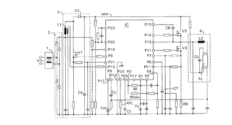
Figure 1 illustrates an electronic ballast for
operating at least one fluorescent lamp, as well as the
actual load circuit, by way of example having only one
fluorescent lamp in this case. The electronic ballast
that is illustrated in based on an electronic ballast
which, in terms of its basic structure and a plurality
of circuit details, is already disclosed in the
document EP-B-0 801 881 mentioned in the introduction,
to which reference can be made here. Known circuit
sections and the functioning thereof which are of
secondary importance in connection with the present
invention are, therefore, anly summarized below and
outlined for reasons of completeness.
A radio frequency filter l, a rectifier bridge 2 and
also a step-up converter 3, which has a charging
inductor Ll, a charging diode D1, a first power
transistor V1 and, as output stage, a storage capacitor
Co, are connected to AC voltage u~. The power
transistor V1 is driven via a control and regulating
circuit IC designed as an integrated circuit. At its
output, the step-up converter 3 provides a stabilized
CA 02311891 2000-06-16
DC voltage, the so-called intermediate circuit voltage
uzw, which is stepped up in comparison with the
rectified power supply voltage. Furthermore, provision
is made of an inverter with a half-bridge circuit,
which is realized here in particular by two further
power transistors V2 and V3, situated in series in
parallel with the output of the step-up converter 3,
and also a bridge capacitor CB. A load circuit 4,
illustrated here with a further inductor L2, a
fluorescent lamp FL and an ignition capacitor Cz, is
connected to the output of the half-bridge circuit V2,
V3.
All the essential control and regulation functions of
the electronic ballast are realized in the control and
regulating circuit IC. For reasons of clarity, the
control and regulating circuit IC is illustrated merely
as a module with external terminals P1 to P24, to which
external components are connected, in Figure 1 and is
illustrated in more detail to supplement that in the
form of a block diagram in Figure 2.
In practical use, a defined power supply of the control
and regulating circuit IC is of considerable
importance; in the present case, however, this can be
assumed to be already known. Therefore, Figure 2
schematically illustrates, in a simplified manner, a
power supply unit IPG, which ensures entirely
satisfactory starting of the functions of the control
and regulating circuit IC and, to that end, is
controlled by the charge state of an externally
connected charging capacitor Ccc. In the steady-state
condition, the power supply of the control and
regulating circuit IC is provided via a pumping diode
DB, connected to the bridge capacitor CB, with a
further external charging capacitor Cp by means of a
two-point regulator TPR. The power supply unit IPG
generates an internal auxiliary voltage IC-BIAS for
supplying the internal circuit units of the control and
CA 02311891 2000-06-16
_ g _
regulating circuit IC and furthermore supplies a
reference voltage Vref. Furthermore, this only being
pointed out, the control and regulating circuit IC
contains an arrangement PFC for controlling the power
factor.
Further control and regulation functions of the control
and regulating circuit IC are also already known per
se. Thus, a drive circuit for the half-bridge circuit
V2, V3 comprises a selection circuit SEL and driver
circuits HSD and LSD, respectively, connected thereto.
A high-frequency pulse train is fed in at a control
input of the selection circuit SEL, which, via the
driver circuits HSD and LSD, respectively, turns on the
power transistors V2 and V3 of the half-bridge circuit
after the manner of a flip-flop alternatively with a
defined blanking interval.
This controlling pulse train is supplied by an
oscillator CCO which is controlled in a
current-dependent manner and has three setting inputs
corresponding to the external terminals P23, P24 and
P3. A first variable resistor RTL is connected to the
terminal P23 and its dimensioning defines, in
particular, the blanking interval of the power
transistors V2 and V3 of the half-bridge circuit. A
variable capacitor Cf is connected to the further
external terminal P24. The third terminal of the
oscillator CCO, connected to the external terminal P3,
is connected to a high-resistance filter network, in
particular formed by non-reactive resistors Rf and
Rfmin and also a further variable capacitor Cc. The
abovementioned external elements and/or the filter
network are connected at the other end to ground or
else to a defined reference voltage (by way of example,
the further description will always refer to ground
here). The dimensioning of these external components
defines the lower and the upper limiting frequency,
respectively, of the oscillator CCO which is controlled
4 CA 02311891 2000-06-16
- 9 -
in a current-dependent manner and the size of the
abovementioned blanking interval. A control signal is
fed via the high-resistance filter network to the
oscillator CCO which is controlled in a
current-dependent manner, said control signal
determining the instantaneous frequency of said
oscillator. This control signal is generated by a
regulating operational amplifier OPR. The latter
compares the reference voltage Vref that is generated
internally with a second input voltage, which is fed in
via the external terminal P5 and corresponds to the
average value of the current flowing through the
half-bridge circuit V2, V3.
The above-described oscillator circuit constitutes a
closed regulating circuit for regulating the load
current flowing in the half-bridge circuit. A rising
load current increases the output voltage of the
regulating operational amplifier OPR, which in turn
controls the oscillator CCO toward a higher pulse
repetition frequency. However, this frequency increase
effects, for its part, a reduction in the load current.
The same applies analogously to the opposite direction,
for a decreasing trend of the load current. The
electronic ballast is also dimmable by means of the
reference voltage Vref being defined correspondingly.
Furthermore, a monitoring function is implemented in
the control and regulating circuit IC in order to
control starting of the lamp, to monitor the state of
the fluorescent lamp FL during steady-state operation,
and also to identify any disturbances that occur. To
that end, provision is made, on the one hand, of a
monitoring circuit MON, which continuously monitors the
load current, that is to say the current flowing
through the half-bridge circuit V2, V3, and, on the
other hand, of a timer PST, which provides a time base
for this monitoring operation.
CA 02311891 2000-06-16
- 10 -
A first internal current source IC is connected via the
external terminal P6 to a further charging capacitor CT
connected to ground. It is activated at the start of
the electronic ballast and charges the external
charging capacitor CT. A signal voltage which rises
linearly up to a final value is formed in the process
at the external terminal P6, which signal voltage is
fed to the control input of the timer PST and provides
the time base for the latter. To that end, said signal
voltage is compared with predetermined threshold values
in the timer PST. When the respective threshold value
is reached, the timer PST outputs a respective
selection signal Sl, S2, S3 or S4 and defines, with the
temporal sequence thereof, specific time segments for
preheating, ignition, subsequent normal operation of
the fluorescent lamp FL and for resetting its driving
in the event of faults that occur, in particular in the
event of ignition failures or a lasting reluctance to
ignite. The meaning of the selection signals S1 to S4
generated by the timer PST will be examined in
connection with the function of the monitoring circuit
MON.
The monitoring circuit MON has a signal input which is
connected via the external terminal P7 and a series
resistor to the output, at low level, of the
half-bridge circuit V2, V3. Consequently, the input
signal fed via the latter to the monitoring circuit MON
is a pulsed signal which is proportional to the current
flowing through the power transistor V3, that is to say
also proportional to the load current. This signal has
superposed on it, as DC bias voltage, the output signal
of a further internal current source IM, which is
activated occasionally by the selection signal S3 of
the timer PST . The level of the bias voltage signal DC
generated by said second internal current source IM is
derived from the current flow through the variable
resistor RTL of the oscillator CCO which is controlled
in a current-dependent manner. To that end, internally
CA 02311891 2000-06-16
- 11 -
within the IC by means of current mirrors, part of the
current flowing through the variable resistor RTL is
fed to the further internal current source IM.
Consequently, by way of the dimensioning of said
external variable resistor RTL, without internal
adaptation or additional external terminals of the
control and regulating circuit IC, it is possible to
adapt the monitoring function of the monitoring circuit
MON to variants of the configuration of the load
circuit 4, in particular specific lamp types and/or
lamp circuits. To put it another way, this measure
makes it possible, despite fixedly predetermined
response thresholds of the monitoring circuit MON for
the preheating and/or ignition voltage, to specifically
configure this monitoring function for the individual
application by way of the dimensioning of the variable
resistor RTL. As a result, without internal
adaptations, the control and regulating circuit IC can
be used for a broad range of circuit alternatives of
the load circuit 4; in particular, tolerances for the
ignition current in specific lamp types can also be
better absorbed.
In principle, one of a plurality of predetermined
threshold values for the load current to be monitored
is in each case activated in a defined manner in the
monitoring circuit MON at specific periods when a lamp
is started and also during normal l.it operation. As
soon as the level of the input signal of the monitoring
circuit MON reaches the instantaneously activated
threshold value, said monitoring circuit emits an
output pulse QM. In the progression over time, this
produces a sequence of momentary output pulses QM which
each trigger control operations in further units of the
control and regulating circuit IC.
This relates, inter alia, to a further regulating
circuit for current regulation. Far this purpose,
CA 02311891 2000-06-16
- 12 -
provision is made of a third internal current source
ISC, the output of which is connected via the external
terminal Pl to the external low-pass filter already
explained. After the manner of a flip-flop, the third
internal current source ISC is respectively set by the
output pulses QM of the monitoring circuit MON and
reset by the selection circuit SEL. Consequently, the
third internal current source ISC charges the external
capacitor Cc of the low-pass filter. In a manner
proportional to the charging of the external charging
capacitor Cc, the input current If changes, which is
fed to the oscillator CCO, which is controlled in a
current-dependent manner, at its control input via the
external terminal P3. In this way, a further closed
regulating circuit is provided, which regulates the
load current cycle by cycle to the respectively
predetermined value which is defined by the
instantaneously activated threshold value of the
monitoring circuit MON. This second regulating circuit
is superordinate to the current regulation described in
the introduction for steady-state operation; it limits
and regulates the load current during starting of the
lamp and also in the event of detected cases of
disturbances.
In context, the function of the monitoring circuit MON
can be illustrated most clearly with reference to the
sequence control during starting of the lamp. If the
electronic ballast is connected to the electricity
supply, the control and regulating circuit IC is
activated, as described, as soon as the switch-on
threshold has been reached. The oscillator CCO which is
controlled in a current-dependent manner then starts
with a predetermined lower limiting frequency and thus
drives the selection circuit SEL, which activates the
half-bridge circuit V2, V3 via the driver circuits HSD
and LSD. The first internal current source IT begins to
charge the external charging capacitor CT and activates
the timer PST. The starting of the lamp begins with a
CA 02311891 2000-06-16
- 13 -
preheating period apt. A corresponding, relatively low
threshold value Mp for the preheating current is
activated in the monitoring circuit MON. The monitoring
circuit MON emits an output pulse QM each time this
threshold value Mp is reached by a pulse of the load
current. These output pulses in each case trigger the
selection circuit SEL and activate the third internal
current source ISC. As a result, the superordinate,
i.e. second, regulating circuit - described in
connection with the function of this current source
ISC - for the current regulation is started. During
this preheating period Opt, the output of a signal
amplifier QPT is switched off. This output can, for
example, be used for controlling a preheating circuit
or for setting a DC bias voltage at the control input
of the monitoring circuit MON, for freely setting the
preheating voltage.
In the further progression, the linearly rising input
voltage of the timer PST reaches a predetermined
preheating level. The preheating period Opt is
concluded and the timer PST generates the first
selection signal S1, which is output to the monitoring
circuit MON and the signal amplifier QPT. A higher
threshold value Mi for the ignition current of the
fluorescent lamp FL is thus activated in the monitoring
circuit MON; an ignition period Dit begins.
Approximately at the same time, preferably immediately
at the beginning of the ignition period Dit, the timer
PST generates a further, the fourth, selection signal
S4, whose trailing edge coincides with a maximum level
of the input voltage of the timer PST being reached.
With this fourth selection signal S4, the second
internal current source IM is activated and,
furthermore, a switch OPRd controlled after the manner
of a flip-flop is enabled. In conjunction with a
further threshold value Md activated in the monitoring
circuit MON, for which threshold value the relationship
~
. CA 02311891 2000-06-16
- 14 -
Mp<Md<Mi
holds true, the monitoring circuit MON monitors the
input signal which is fed to it, and i.s proportional to
the load current, with regard to this threshold and, in
a manner dependent thereon, supplies the further output
pulses QM1. With each of these pulses, the
abovementioned switch OPRd is initially set and in each
case reset by the output signal of the selection
circuit SEL. When the switch OPRd is switched on,
ground potential is applied to the noninverting input
of the regulating operational amplifier OPR, said input
being connected to the external terminal P5. In this
way, the limiting of the load current by the regulating
operational amplifier OPR is deactivated for the
duration of the ignition period Dit, that is to say the
ignition voltage is not limited.
In the normal case, the fluorescent lamp FL ignites
within a predetermined time after only a few ignition
attempts. The peak value of the load current then
automatically reverts to a normal operational value
and, in the process, no longer reaches the threshold
value Mi of the monitoring circuit MON; no further
output pulses QM are generated.
The timer PST continues to run, however. Its rising
input voltage initially passes through a predetermined
ignition level and finally reaches a maximum level
which initiates resetting of the timer PST. When this
maximum level has been reached, the timer generates the
output signal S3, which, on the one hand, activates a
threshold value Mo in the monitoring circuit MON, which
threshold value is not reached by the evaluated load
current during normal lit operation of the fluorescent
lamp FL; in other words no further output pulses QM are
generated by it. On the other hand, the second internal
current source IT assigned to the timer PST is switched
off by the third selection signal S3. The charging
°°
. CA 02311891 2000-06-16
- 15 -
capacitor CT connected to said second internal current
source begins to discharge, that is to say the input
signal fed to the timer PST falls to a constant level
which is held during normal lit operation. However, as
soon as the defined ignition period Dit has elapsed,
the timer PST generates a further, the second,
selection signal S2. The latter is held until the input
signal of the timer PST passes through the ignition
level again as it falls. This pulse duration of the
second selection signal S2 defines a disconnection
period Ost which follows the ignition period fit and in
which the disconnection of the electronic ballast is
prepared in the event of a fault.
For the implementation of this function, a
disconnection unit with a counter CTR and a
disconnection circuit SDL is provided. The counter CTR
is reset both by the rising edge and by the falling
edge of the second selection signal S2. It is fed the
output pulses QM of the monitoring circuit MON as
counting pulses. In the event of a normal starting
operation, it reaches its final value after four
counting pulses, for example, and then activates the
internal current source IT. In the further progression,
the leading edge of the second selection signal S2
resets the counter CTR and preparatorily enables the
disconnection circuit SDL. The number of vain ignition
attempts or the number of output pulses QM that then
occur is now counted. If the counter CTR reaches its
final value in the case of a lamp that is reluctant tn
ignite, it activates the preparatorily enabled
disconnection circuit SDL. The latter thereupon
inhibits the selection circuit SEL, inter aila, and
thereby interrupts the driving of the half-bridge
circuit V2, V3. In an analogous manner, in the event of
failure of the ignition of the fluorescent lamp FL
during normal lit operation, the timer is activated
again, renewed ignition attempts are evaluated in the
monitoring circuit MON and output pulses OM are
" - CA 02311891 2000-06-16
- 16 -
generated in the process. This again leads to the
above-described disconnection of the electronic ballast
after repeated vain ignition attempts. The hysteresis
introduced by virtue of this measure suppresses
momentary disturbances and leads to enhanced
interference immunity of the electronic ballast.
For the sake of completeness, it shall be added that
the control and regulating circuit IC is, finally, also
designed for adaptation to changes in the load current
in a relatively broad tolerance range. Such changes may
occur in particular in the dimming state in the case of
multi-lamp applications or else in the case of critical
lamp tolerances, e.g. caused by aged, high-resistance
lamp filaments. These situations can lead to the
regulating operational amplifier OPR no longer
operating within its defined regulating range. This
state is detected by a further comparator COMP, which
is connected to the external terminal P1 by its
noninverting input and whose inverting input is fed an
internally generated comparison voltage Vcc', which is
reduced considerably, for example by 25~, compared with
the voltage occurring in the normal operating state
across the charging capacitor Ccc. If such an operating
state occurs, the comparator COMP outputs a control
signal to the monitoring circuit MON, which control
signal sets, in said monitoring circuit, a state in
which all the reference levels Mp, Mi, Mdo and Mo are
considerably reduced. Therefore, the monitoring circuit
MON then operates satisfactorily even at relatively low
lamp currents.