Note: Descriptions are shown in the official language in which they were submitted.
CA 02312129 2000-06-22
-1-
1 c~42; ID: WHITTAKER, E,.l
HIGH SPEED LEVEL SHIFT CIRCUIT FOR LOW VOLTAGE OUTPUT
FIELD OF THE INVENTION
The present invention relates to a method and apparatus for high speed
s level shifting to provide a low voltage output, and a system incorporating
the same.
BACKGROUND TO THE INVENTION
Logic signals at very high speed are often processed using bipolar
Current Mode Logic (CML) - a signalling system involving small voltage
to swings (typically 250mV) referenced to the positive supply of the
integrated circuit (IC). Output interface levels from an IC using this logic
are generally specified with a greater signal swing than 250mV.
For a bipolar transistor to operate at speed it is necessary that its
collector
base junction does not enter forward conduction. Therefore, in order to
is allow increased signal swing on the output stage, the logic signals which
drive it have to be level shifted from the positive rail reference down to a
lower voltage. The more the signal can be shifted the greater the
potential output swing.
Known attempts to level shift very high speed logic signals from a positive
2o power rail reference down to a level as close as possible to a ground or
negative rail, however, have encountered a number of problems.
Use of complementary vertical PNP transistors in the signal path slowed
the signal since PNP's are inherently slower than NPN's. Their use also
added considerably to the complexity of the semiconductor process since
2s extra process steps were required in their fabrication.
Use of NPN diode level shifters was also considered. However this
approach did not take account of power supply variation and required
circuit complexity to allow for the temperature variation of the forward
voltage drop of the diode junction. Tolerancing these circuits over
3o temperature and power rail variation was therefore difficult since, in
general, complexity in the signal path leads to slow circuits.
CA 02312129 2000-06-22
.-.
-2-
OBJECT OF THE INVENTION
The present invention seeks to provide an improved method and
apparatus for high speed level shifting for low voltage output.
SUMMARY OF THE INVENTION
s According to a first aspect of the present invention there is provided an
electronic circuit arranged to receive a common mode input data signal
referenced to a first positive reference voltage supply and to provide an
intermediate data signal referenced to a second positive reference voltage
supply, wherein said second reference voltage is lower than said first
io reference voltage.
Preferably, all transistors through which data signals pass between said
input data signal and said intermediate data signal are NPN transistors.
Advantageously, level shifting of very high speed logic signals from the
positive power rail reference down to a level as close as possible to the
is ground power rail without use of vertical PNP transistors in the signal
path
avoids slowing the signal since PNP's are inherently slower than NPN's,
and avoids adding considerable complexity of the semiconductor
fabrication process that would arise from additional steps required to form
vertical PNP's.
2o Advantageously, signals referenced to the ground rail may be used to
drive a very fast long tailed pair output stage with minimal loss of voltage
headroom and hence best efficiency.
Advantageously, the present invention maximises the drive capability of
such a high speed output signal without invoking any additional power
2s rails or any special process steps in the fabrication of the IC.
Advantageously, the circuit may operate from a single external power
supply.
Preferably said input data signal, and intermediate data signal are
common mode logic signals.
3o Preferably said first and second voltages are both positive.
CA 02312129 2000-06-22
-3-
Advantageously this does not require provisioning of a negative power rail
which would be expensive, require more power, and impose greater
voltage stress on the integrated chip.
Preferably the maximum voltage of said intermediate signal does not
s exceed said second reference voltage.
Preferably said second reference voltage is maintained within lower
tolerances than said first reference voltage.
Preferably said second reference voltage is provided from a band gap
supply.
to Advantageously, the circuit takes account of power supply variation and
overcomes the problems associated with temperature variation of the
forward voltage dcp associated with use of diode junction: tolerancing
these circuits over temperature and power rail variation is more
straightforward since the circuitry involved is simpler.
is In a preferred embodiment, said first circuit comprises a first and second
input circuits, a sensing element, and a current mirror circuit.
In a preferred embodiment the circuit additionally comprises a second
circuit arranged to regenerate said intermediate data signal whereby to
provide an output data signal.
2o Preferably, said second circuit comprises a long-tailed pair.
The arrangement may also comprise a third circuit arranged to provide a
second output data signal referenced to said second reference voltage
supply and having high current drive.
Preferably said high current drive is drawn from said first reference
2s voltage supply.
Preferably said third circuit comprises a feedback circuit, whereby to
maintain said second output data signal within tolerances.
The arrangement may also comprise a laser modulator circuit arranged to
provide an optical output data signal responsive to receipt of said output
3o data signal.
CA 02312129 2000-06-22
-4-
According to a second aspect of the present invention there is provided a
laser modulator package assembly comprising an electronic circuit
arrangement according to the first aspect of the present invention.
Preferably said electronic circuit arrangement comprises a laser modulator
s circuit arranged to provide an optical output data signal responsive to
receipt of said output data signal.
According to a third aspect of the present invention there is provided an
optical transmitter circuit board comprising a laser modulator package.
According to a fourth aspect of the present invention there is provided a
io telecommunications system comprising an electronic circuit arrangement.
The invention also provides for a system for the purposes of digital signal
processing which comprises one or more instances of apparatus
embodying the present invention, together with other additional
apparatus.
is The invention is also directed to a method by which the described
apparatus operates and including method steps for carrying out every
function of the apparatus.
In particular, according to a fifth aspect of the present invention there is
provided a method of level shifting an input data signal comprising the
2o stages of providing said input data signal referenced to a first positive
reference voltage supply, generating an intermediate data signal
referenced to a second positive reference supply responsive to receipt of
said input data signal, wherein said second reference voltage is lower
than said first reference voltage.
2s In a preferred embodiment, the method additionally comprises the steps
of generating an output data signal with high current drive and referenced
to said second positive reference voltage supply with high current drive
responsive to receipt of said intermediate data signal,
In a further preferred embodiment, the method additionally comprises the
3o steps of providing an optical output data signal responsive to receipt of
said intermediate data signal.
CA 02312129 2000-06-22
-5-
The preferred features may be combined as appropriate, as would be
apparent to a skilled person, and may be combined with any of the
aspects of the invention.
BRIEF DESCRIPTION OF THE DRAWINGS
s In order to show how the invention may be carried into effect,
embodiments of the invention are now described below by way of
example only and with reference to the accompanying figures in which:
Figure 1 shows a first circuit in accordance with the present invention;
Figure 2 shows a second circuit in accordance with the present invention
Io arranged to drive a Low Voltage Differential Signal (LVDS) buffer;
Figure 3 shows a second circuit in accordance with the present invention
arranged to drive a laser modulator.
DETAILED DESCRIPTION OF INVENTION
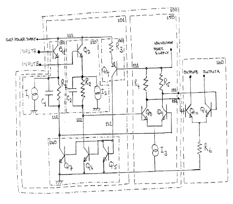
Referring first to Figure 1, there is shown a first embodiment of a high-
is speed level shift circuit for low voltage output.
The high speed level shift circuit 100 comprises a re-referencing stage
101 and a regenerating buffer stage 150. In the arrangement shown, the
level shift circuit is coupled to an output stage 160.
The re-referencing stage 100 comprises first and second input stages
20 110, 120, sensing element 130, and current mirror 140.
Input stage 110 comprises a connection to the chip power rail 111
(typically 3.3V ~0.3) and a data signal input INPUTA and a signal output
112. It comprises a NPN transistor Q1, resistor R1 capacitor C1, and
current source 11. The base connection of Q1 is connected to the data
2s input INPUTA; the collector of Q1 is connected to the chip power rail 111.
Resistor R1 is connected in series between the emitter of Q1 and the
output port 112. Capacitor C1 is connected in parallel across resistor R1.
Current source 11 is connected to the emitter of Q1.
Input stage 120 is similarly configured with corresponding elements Q2,
3o R2, C2, and 12.
CA 02312129 2000-06-22
-6-
Turning now to the sensing element 130, this comprises a resistor R3 and
PNP transistor Q4, resistor R3 being connected in series between the
chip power rail 111 and the emitter of Q4. The base of Q4 is connected to
low voltage power rail 131 whilst the collector of Q4 is connected to the
s current mirror 140 via connection 132. Q4 may be a lateral PNP
transistor.
The current mirror 140 comprises three NPN transistors Q5, Q6, and Q7.
The base of each of these transistors is connected to output 132 of the
sensing circuit 130 as is the collector of transistor Q5. Collectors of Q6,
io Q7 are connected to outputs 122, 112 of input stages 120, 110
respectively. Emitters of each of the three transistors are connected to
ground.
The regenerating buffer stage 150 comprises a long-tailed pair comprising
two resistors R4, R5, two NPN transistors Q8, Q9, and a current supply
is 13. The base of Q8 is connected to the output 122 of input stage 120 and
correspondingly the base of Q9 is connected to output 112 of input stage
110. The collector of Q8 is connected via resistor R4 to the low voltage
power rail 131; similarly the collector of Q9 is connected via resistor R5 to
the low voltage power rail 131. The emitters of both Q8 and Q9 are
2o connected via current supply R3 to ground. Two output ports are
provided 151, 152 connected to the collector of Q9 and Q8 respectively.
The output stage 160 comprises a pair of NPN transistors Q10 and Q11
and resistor R6. The bases of Q10, Q11 are connected to ports 152, 151
respectively whilst the emitters are connected via resistor R6 to ground.
2s The collectors of Q11, Q10 are connected to output ports OUTPUTA,
OUTPUTB respectively.
The regenerating buffer stage 150 is used to set the minimum voltage
required for the output stage 160 to operate and also sets the voltage
across resistor R6.
3o Output stage 160 is used to set the voltage and power levels at the two
outputs OUTPUTA and OUTPUTB.
In operation, an input signal is provided on pins INPUTA and INPUTB.
This signal is typically a differential Current Mode Logic (CML) signal with
a swing of about 250mV with respect to the positive supply rail. This
CA 02312129 2000-06-22
",..
_7_
drives emitter followers Q1 and Q2 which are biased via the two current
sources 11 and 12. The emitters drive two resistors, R1 and R2, the DC
voltage drops across which are set by the current flowing through the
mirror transistors Q5, Q6. The purpose of this voltage drop is to match the
s signal from the emitter followers into the long tailed pair formed by Q8 and
Q9. Capacitors C1 and C2 give a high frequency path past R1 and R2 to
overcome the capacitive loading imposed by Q8 and Q9. The voltage
swing on the collectors of Q8 and Q9 is restricted to about 250mV and
with the feed from Q1 and Q2 both are fully switched. In order to prevent
to the saturation of Q8 or Q9 the drive to the bases should not exceed the
positive power rail for Q8 and Q9. This will still reverse the collector base
junctions of Q8 or Q9 by 250mV but this does not substantially impinge on
operating speed and is the normal operating condition for CML circuits
anyway. Examining the circuit it is apparent that the required current, Id~
Is through R1 and R2 is given by:
lUposl Vpos2 ~ Vbe
R1
where Vbe is the forward emitter base voltage of Q1 or Q2 VPos, is the
power rail 111 supply voltage, and VPos2 is the low voltage power rail 131
supply voltage.
2o The requirements on the drive to Q8 and Q9 are not particularly stringent.
A match to within 50mV of the ideal is sufficient and to a first
approximation a PNP forward voltage drop may be matched to a NPN
drop (i.e. with appropriate geometries the magnitude of their Vg's may be
considered the same for a given operating current). A low speed circuit
2s formed by the slow lateral PNP transistor, Q4, and the resistor R3 senses
the difference in the potential ((VPos, -VPo52) - Vbe). In the case where R1 =
R2 = R3 the low speed circuit sets up a current in the collector of Q4,
exactly matching the required current in R1 and R2. It is then a simple
matter of mirroring this current via Q5, Q6, and Q7 in order to set up the
3o correct conditions on the bases of Q8 and Q9.
In some applications it may be advantageous to add further circuitry to
allow for the finite gain of the transistors and the effects of base width
modulation with collector voltage (Early effect). Such techniques are well
known in the art.
CA 02312129 2000-06-22
_$_
The drive requirements to the bases of Q10 and Q11 dictate the choice of
Vp~52. It is apparent from Figurel that Vpos2 programs the current steered by
Q10 and Q11. In the case where the base current drawn by Q10 and
Q11 makes minimal impact on the voltage on Q8 and Q9 collectors
s respectively, the voltage, V6, across R6 is given by equation (2).
V6 = Vpos2 - Vbe (2)
where Vbe is the voltage between base and emitter of transistor Q10 or
Q11.
The current, I, out through Q10 and Q11 collectors is given by equation
io (3).
I - (Vpos2 Vbe)' RV 3
It is clearly possible to vary the current output by changing Vpos2. By
assigning an appropriate temperature dependence to Vpo52, the current, I,
may be made to have any required temperature characteristic.
is The output voltage of Q10 and Q11 may safely swing down to a minimum,
~min~ given in equation (4).
Vmin - (Vpos2 Vbe) + Vsat
where Vsa, is the minimum collector emitter voltage of Q10 and Q11 below
which the transistors saturate and performance is degraded.
2o In summary, the re-referencing circuit 101 is arranged to receive a pair of
common mode logic signals on its data inputs INPUTA, INPUTB
referenced to the positive power rail 111 and re-references these inputs to
a second reference voltage Vpos2. In addition, by virtue of its connection
via Q4 to the low voltage bandgap supply, the circuit ensures that the
2s voltage of the output signals is normally less than that of the low-voltage
supply 131. This ensures that the intermediate output signals at 112, 122
have a constant common mode referenced to the ground rail and lower
than the bandgap supply voltage, Vpo52 on rail 131.
The regenerating buffer circuit 150 is arranged to regenerate the
3o intermediate output signals provided by the initial re-referencing circuit
101, re-referenced to the low voltage bandgap supply, Vpos2, and ensures
CA 02312129 2000-06-22
_g_
that the maximum voltage of the output signals does not exceed that of
the low-voltage supply.
Referring now to Figure 2, there is shown the design of an LVDS output
driver, using the level shift circuit 100.
s This circuit comprises an additional control loop 210, comprising four
resistors R7-R10, amplifier AMP, and NPN transistor Q12. Resistors Rg,
R10 are connected in parallel from the inverting input of the amplifier AMP
to data outputs OUTPUTA and OUTPUTB respectively of output stage
160. The non-inverting input of the amplifier is connected to a + 1.2V
to supply whilst its output is connected to the base of transistor Q12. The
collector of transistor Q12 is connected to chip power rail Vpos,. Resistors
R7, R8 are arranged in parallel to provide paths from the emitter of
transistor Q12 to OUTPUTB and OUTPUTA respectively.
Control loop 120 stabilises the mean output voltage to 1.2v as required by
is the LVDS specification. This is provided by sensing the mean voltage of
the outputs with two high value resistors R9 and R10 (where Rg, R10 »
R7, R8) and comparing with a reference 1.2V source in the amplifier, AMP
which drives the emitter follower of Q12. VPos2 is set such that the output
swing on nodes OUTPUTA and OUTPUTB is 300mV (in the middle of the
2o specification for output swing) when loaded with an external 100 ohm
load.
If the current drawn by the bases of Q10, Q11 should increase such that
appreciable drops across R4, R5 would result then it is possible to
increase VPos2 by one Vbe and use NPN emitter followers on the output of
2s Q8/Q9 collectors to overcome this problem.
When driving a laser diode it is normal to have standing DC current which
sets the diode at its threshold, and an additional superposed pulse
modulation. The amplitude of both these components varies widely from
diode to diode - even of the same type and so these have to be
3o programmed for each diode.
Figure 3 shows the design of a pulse modulator for a laser diode D1
driven from a 3.3V supply (VPos,) with variable modulation current. The
arrangement comprises a high speed level shift circuit 100 and a laser
diode output stage 300.
CA 02312129 2000-06-22
-10-
s
The laser diode output stage comprises a laser diode D1, five NPN
transistors Q10-Q14, resistor R7, and two current sources 14, 15.
The bases of Q13, Q14 are coupled to data outputs 151, 152 respectively;
collectors of Q13, Q14 are coupled to the chip power rail 111; and
emitters coupled to ground via power supplies 14, 15 respectively.
The bases of Q10, Q11 are coupled to the emitters of Q13, Q14
respectively; emitters of both Q10 and Q11 are coupled to the collector of
Q12, the emitter of which is coupled via resistor R7 to ground.
The collector of Q10 is coupled to the chip power rail 111; the collector of
to Q11 which carries the regenerated input signal from INPUTA, is coupled
to ground via laser diode D1.
In this arrangement emitter followers Q13, Q14 are placed between R4,
R5 and Q10, Q11 respectively, as described above. This allows the
driving of higher current laser diodes, but is not mandatory for more
is sensitive laser diodes. The current through the output stage in this
arrangement is set by a programmable current source, comprising NPN
transistor Q15 and resistor R7. The voltage VB,AS on Q15 base sets the
output current and may be adjusted for each laser diode. The only
performance penalty of this arrangement over that in Figure 1 is the
2o additional headroom needed to accommodate the current source.
Effectively this is the saturation voltage, Vsa,, of Q12.
This circuit arrangement facilitates collocation of the driver circuit with
the
laser diode itself in the same package. If the driver is mounted
exceptionally close to the laser the electrical interface to the laser can be
2s kept simple thereby saving power in the laser driver. This power saving is
certainly necessary if they are to be collocated: lasers work best when
cool. By saving power in the driver it is possible to mount the driver close
to the laser without needing to use, for example, Pettier cooling devices to
refrigerate the whole assembly.
3o The power saving comes about because of the avoidance of the difficulty
of driving fast signals to a laser over any distance. The reason is the low
impedance presented by the laser diode: typically a few ohms. To drive
fast signals over any distance it is necessary to use a transmission line
terminated in the natural impedance of the transmission line. Typically,
CA 02312129 2000-06-22
._
-11 -
the impedance of a transmission line is 50 ohms although lower
impedances may be made (though not down to the impedance of the
diode). The diode end of the transmission line has to match the line
impedance. This is done by adding resistance in series with the diode to
s raise the resultant impedance to that of the line. This series resistor is
where the power is wasted and the additional power has to come from the
laser driver. Typically, commercial high speed test gear and cabling is
built for 50 ohms, thus if laser and driver are to be supplied as separate
modules this is very much the preferred impedance since users can hook
to the two together and/or evaluate them individually using standard
equipment. The cabling, and special high frequency connectors would all
add cost to the arrangement. The increased power required from the
laser driver needs a separate integrated circuit, usually in the very
expensive Gallium Arsenide process, since that is better suited than
is silicon to such an increased level of output. The additional electrical
power has to be supplied to the laser system and the resultant increase in
heat dissipated. And, of course, one module takes less space than two
linked by cable with connectors on them.
Furthermore, purchasers of such apparatus would prefer to purchase off-
2o the-shelf circuits arranged to accept standard logic signal in, and give
optical signals out, rather that be left the task of coupling lasers to their
drivers themselves
Any range or device value given herein may be extended or altered
without losing the effect sought, as will be apparent to the skilled person
2s for an understanding of the teachings herein.