Note: Descriptions are shown in the official language in which they were submitted.
CA 02312140 2000-06-22
TITLE OF THE INVENTION
Charge separation Type Heterojunction Structure and Manufacturing Method
Therefor
BACKGROUND OF THE INVENTION
Field of the Invention
This invention relates to a charge separation type heterojunction structure
used
in e.g., a solar cell or a light emitting diode and which has fullerene as a
portion of a
constituting material thereof. This invention also relates to a manufacturing
method
for the charge separation type heterojunction structure.
Description of Prior Art
Up to now, a silicon pn junction semiconductor etc has been extensively used
in e.g., a solar cell or a light emitting diode. Of late, the energy
conversion efficiency
of the silicon pn junction semiconductor has been improved appreciably in
comparison
with that when the silicon pn junction semiconductor was initially devised.
Among the materials for the solar cell, there is e.g., titanic in addition to
silicon.
Recently, however, fullerene, as a carbon compound, has attracted attention.
The
features of fullerene is hereinafter explained in connection with the
discovery and the
history of development thereof.
Fullerene is a series of carbon compounds composed only of carbon atoms, as
is diamond or graphite. The existence of fullerene was confirmed in eighties.
That is,
it was found in 1985 in a mass analysis spectrum of a cluster beam by laser
ablation
1
CA 02312140 2000-06-22
of carbon. It was, however, five years later that the manufacturing method in
reality
was established. Specifically, a manufacturing method for fullerene (C~~) by
arc
discharge of a carbon electrode was first found in 1990. Since then, fullerene
is
attracting notice as a carbonaceous semiconductor material (see Kratschmer,
W.,
Fostiropoulos, K, Huffman D.R. Chem. Phys. Lett. 1990, 170, 167. Kratschmer,
W.
Lamb L.D., Fostiropoulod. K, Huffman, D.R. Nature 1990, 347,354).
Fullerene is a spherical carbon C" (n = 60, 70, 76, 78, 80, 82, 84, w) which
is
a molecular aggregate resulting from spherical aggregation of an even number
not less
than 60 of carbon atoms. Representatives of the fullerenes are C~~, with 60
carbon
atoms and C.,o with 70 carbon atoms. Of these, the Coo fullerene is of a
polyhedral
structure termed truncated-icosahedron obtained from an icosahedron by
truncating
each of the twelve vertices. Hence, each vertex is replaced by a pentagon.
Thus, the
C~~ fullerene has a molecular structure of what may be termed a soccer ball
type in
which its 60 apices are all occupied by carbon atoms. On the other hand, C.,o
has what
may be termed a rugby ball type molecular structure.
In a Coo crystal, Cbo molecules are arranged in a face-centered cubic
structure.
It has a band gap of approximately 1.6 eV and may be deemed as a
semiconductor.
In an intrinsic state, it has an electrical resistivity of approximately 10'
SZcm. It has
a vapor pressure of approximately 1 m Torr at 500°C and, on
sublimation, is capable
of vapor depositing a thin film. Not only Coo but other forms of the fullerene
are
readily vaporized in vacuum or under reduced pressure and hence are able to
yield an
2
CA 02312140 2000-06-22
evaporated film easily.
However, the molecules of fullerene forms, such as C~,~, or C~~, the most mass-
producible, are of zero dipole moment, such that evaporated films produced
therefrom
are fragile in strength, because only the van der Waal's force acts between
its
molecules. Thus, if the evaporated film is exposed to air, molecules of oxygen
or
water tend to be diffused and intruded into the gap between the fullerene
molecules
(Fig.2), as a result of which the evaporated film is not only deteriorated in
structure but
adverse effects may be occasionally produced in its electronic properties.
This fragility
of the fullerene poses a problem in reference to device stability when
applying the
fullerene to fabrication of a thin-film electronic device.
For overcoming the weak points the fullerene polymer film, described above,
the method of producing a so-called fullerene polymer consisting in
polymerizing
fullerene molecules has been proposed. Typical of these methods is a method of
forming a fullerene polymer film by light excitation (see (a) Rao, A.M., Zhou,
P,
Wang., K. A, Hager., G. T., Holden, J. M., Wang, Y., Lee, W.T., Bi, X, X.,
Eklund,
P.C., Cornet, D. S., Duncan, M. A., Amster, J. J. Science 1993, 256995, (b)
Cornet,
D. C., Amster I. J.,Duncan, M. A., Rao A. M., Eklund P. C., J. Phys. Chem.
1993,
97,5036, (c) Li. J., Ozawa, M., Kino, N, Yoshizawa, T., Mitsuki, T., Horiuchi,
H.,
Tachikawa, O; Kishio, K., Kitazawa, K., Chem. Phys. Lett. 1994, 227, 572].
In these methods, in which light is illuminated on a previously formed
evaporated fullerene film, numerous cracks tend to be formed in the film
surface due
3
CA 02312140 2000-06-22
to volumetric contraction produced on polymerization, so that produced films
are
problematic in strength. Moreover, it is extremely difficult to form a uniform
thin film
of a large surface area.
It has also been known to apply pressure or heat to fullerene molecules or to
cause collision of fullerene molecules against one another. It is however
difficult to
produce a thin film, even though it is possible to form a film (see, for a
molecule
collision method, (a) Yeretzian, C., Hansen, K., Diedrich, F., Whetten, R. L.,
Nature
1992, 359,44, (b) Wheten, R. L., Yeretzian, C., Int. J. Multi-layered optical
disc. Phys.
1992, B6,3801, (c) Hansen, K., Yeretzian, C., Whetten, R.L., Chem. Phys. Lett.
1994,
218,462, and (d) Seifert, G., Schmidt, R., Int. J. Multi-layered optical disc.
Phys.1992,
B6,3845; for an ion beam method, (a) Seraphim S., Zhou, D., Jiao, J. J.
Master. Res.
1993, 8,1995, (b) Gaber, H., Busmann, H. G., Hiss, R., Hertel, I. V., Romberg,
H.,
Fink, J., Bruder, F., Brenn, R.J. Phys. Chem., 1993, 97,8244; for a pressure
method,
(a) Duclos, S.J., Brister, K., Haddon, R.C., Kortan, A. R., Thiel, F.A..
Nature
1991,351,380, (b) Snoke, D.W., Raptis, Y.S., Syassen, K. 1 Phys. Rev. 1992,
B45,
14419, (c) Yamazaki, H., Yoshida, M., Kakudate, Y., Usuda, S., Yokoi, H.,
Fujiwara,
S., Aoki, K., Ruoff, R., Malhotra, R., Lorents, D.J., Phys. Chem. 1993,
97,11161, and
(d) Rao, C.N.R., Govindaraj, A., Aiyer, H. N., Seshadri, R.J. Phys. Chem.
1995,
99,16814).
Noteworthy as a fullerene polymerization method or film-forming method,
which should take the place of the above-enumerated fullerene polymerization
4
CA 02312140 2000-06-22
methods, is the plasma polymerization method or the micro-wave (plasma)
polymerization method, previously proposed by the present inventors in e.g.,
Takahashi, N., Dock, H. or in Matsuzawa, N., Ata M.J., Appl. Phys. 1993,
74,5790.
The fullerene polymer film, obtained by these methods (see Figs.3 and 4), are
thin
films produced by polymerization of the fullerene molecules through an
electronic
excited state. It is appreciably increased in strength in comparison with the
evaporated
thin fullerene film, dense and high in pliability. Since the fullerene polymer
film is
scarcely changed in its electronic properties in vacuum or in air, it may be
premeditated that its dense thin-film properties effectively suppress
diffusion or
intrusion of oxygen molecules into the inside of the film. In reality,
generation of
fullerene polymer consisting the thin film by these methods may be
demonstrated by
the time-of-flight mass spectrometry.
Irrespective of the type of the plasma method, electron properties of a
fullerene
polymer film possibly depend appreciably on its polymerization configuration.
In
reality, the results of mass spectrometry of the C~~ polymer film, obtained by
the
micro-wave plasma method, bear strong resemblance to those of the Coo argon
plasma
polymer thin film, previously reported by the present inventors [see Ata, M.,
Takahashi, N., Nojima, K., J. Phys. Chem. 1994, 98, 9960, Ata, M., Kurihara,
K.,
Takahashi, J. Phys., Chem., B., 1996, 101,5].
The structure of the fullerene polymer may be estimated by the pulse laser
excited time-of-flight mass spectrometry (TOF-MS). In general, there is known
a
CA 02312140 2000-06-22
matrix assist method as a method for non-destructive measurement the high
molecular polymer. However, lacking the solvent capable of dissolving the
fullerene
polymer, it is difficult to directly evaluate the actual molecular weight
distribution of
the polymer. Even with the mass evaluation by Laser Desorption Ionization Time-
of-
Fight Mass Spectroscopy (LDITOF-MS), it is difficult to make correct
evaluation of
the mass distribution of an actual fullerene polymer due to the absence of
suitable
solvents or to the reaction taking place between C~,o and the matrix molecule.
The structure of the Coo polymer can be inferred from the profile of a dimer
or
the peak of the polymer of LDITOF-MS, as observed in the ablation of such a
laser
power as not to cause polymerization of C6~,. For example, LDITOF-MS of a C~~
polymer film, obtained with a plasma power of e.g., SOW, indicates that the
polymerization of Coo molecules is most likely to take place through a process
accompanied by loss of four carbon atoms. That is, in the mass range of a
dimer, Clzo
is a minor product, whilst C,16 is produced with the highest probability.
According to semi-empiric Coo dimer calculations, this Cl,b may be presumed
to be D2h symmetrical Cl6 shown in Fig.lO. This may be obtained by Csg
recombination. It is reported that this C5g is yielded on desorption of CZ
from the high
electronic excited state including the ionized state of Coo [(a) Fieber-
Erdmann, M., et
al., Phys. D. 1993, 26,308 (b) Petrie, S. et al., Nature 1993,356,426 and (c)
Eckhoff,
W. C.,Scuseria, G. E., Chem. Phys. Lett. 1993, 216,399].
If, before transition to a structure comprised of two neighboring five-
membered
6
CA 02312140 2000-06-22
rings, this open-shell Csx molecules are combined with two molecules, C1,6
shown in
Fig.lO is produced. However, according to the notion of the present inventors,
it is
after all the [2+2] cycloaddition reaction by the excitation triplex mechanism
in the
initial process of the C~,~, plasma polymerization. The reaction product is
shown in
Fig.9. On the other hand, the yielding of C,1~, with the highest probability
as mentioned
above is possibly ascribable to desorption of four spa carbons constituting a
cyclobutane of (C~o)' yielded by the [2+2] cycloaddition from the excited
triplet
electronic state of C~~, and to recombination of two Csx open-shell molecules,
as shown
in Fig.6.
If a powerful pulsed laser light beam is illuminated on a Coo fine crystal on
an
ionization target of TOF-Ms, as an example, polymerization of fullerene
molecules
occurs through the excited electronic state, as in the case of the micro-wave
plasma
polymerization method. At this time, ions of CS~, CS6 etc are also observed
along with
peaks of the C6~ photopolymer.
However, since no fragment ions, such as Csga+ or C''+ are observed, direct
fragmentation from C~~3+ to CSx2+ and to CZ+, such as is discussed in the
literature of
Fieber-Erdmann, cannot be thought to occur in this case. Also, if Coo is
vaporized in
a CZ F4 gas plasma to form a film, only addition products of fragment ions of
F or CZF4
of Coo are observed in the LDITOF-MS, while no Cro polymer is observed. Thus,
the
LDITOF-MS, for which no C« polymer is observed, has a feature that no CS$ nor
C5~
ions are observed. These results of observation support the fact that C Z loss
occurs
7
CA 02312140 2000-06-22
through a Cbo polymer.
The next problem posed is whether or not the C~ loss is directly caused from
1,
2- (C~,o) ~ produced by the (2+2] cycloaddition reaction shown in Fig.6. Murry
and
Osawa et al proposed and explained the process of structure relaxation of 1, 2-
(C~,o)
2 as follows ((a) Murry, R.L. et al, Nature 1993, 366,665, (b) Strout, D.L. et
al, Chem.
Phys. Lett. 1993, 214,576, Osawa, E, private letter].
Both Murry and Osawa state that, in the initial process of structure
relaxation
of 1, 2- (C6o)2, Cmo (d) of Fig.l3 is produced through Cl2o (b) of Fig.ll,
resulting from
cleavage of the 1, 2 - C bond, having the maximum pinch of the cross-linked
site,
from Cl~o (c) of Fig.l2 having the ladder-like cross-linking by Stone-Wales
transition
(Stone, A.J., Wales, D. J., Chem. Phys. Lett. 1986,128, 501, (b) Saito, R.
Chem. Phys.
Lett.1992,195,537). On transition from Clao (c) of Fig.l2 to C,ZO (b) of
Fig.ll, energy
instability occurs. However, on further transition from Cl2o (c) of Fig.l2 to
Cl2o (d) of
Fig.l3, the stabilized state is restored.
Although it is not clear whether the nC2 loss observed in the polymerization
of
C60 by plasma excitation directly occurs from 1, 2 - (Cbo) thought to be its
initial
process or after certain structure relaxation thereof, it may be premeditated
that the
observed CllB assumes the structure shown in Fig.l4 by desorption of C~ from
C,2o (d)
of Fig.l3 and recombination of dangling bonds. Also, C,1~ shown in Fig.lS is
obtained
by desorption of two carbon atoms of the ladder-like cross-linking of C"x of
Fig.l4
and recombination of bonds. Judging from the fact that there are scarcely
observed
8
CA 02312140 2000-06-22
odd-numbered clusters in the dimeric TOF-MS, and from the structural
stability, it
may be presumed that the loss in C~ is not produced directly from 1,2 -
(C~,~,) 2, but
rather that it is produced through C1~~ (d) of Fig.l3.
Also, Osawa et al states in the above-mentioned literature that DSd
symmetrical
C,~~, structure is obtained from C,~~ (a) through structure relaxation by
multi-stage
Stone-Wales transition. However, insofar as the TOF-MS of the C~,~ polymer is
concerned, it is not the structure relaxation by the multi-stage transition
reaction but
rather the process of structure relaxation accompanied by C2 loss that governs
the
formation of the polymer by plasma irradiation.
In a planar covalent compound in general, in which a ~t-orbital crosses the a-
orbital, spin transition between 1(~ - rt*) - 3(n - 7c*) is a taboo, while it
is allowed if,
by vibration-electric interaction, there is mixed the Q-orbital. In the case
of Cbo, since
the ~-orbital is mixed with the Q-orbital due to non-planarity of the ~
covalent system,
inter-state crossing by spin-orbital interaction between 1(~ - n*) and 3(~ -
~*)
becomes possible, thus producing the high photochemical reactivity of C6~.
The plasma polymerization method is applicable to polymerization of Coo
molecules. However, the polymerization between G,~ molecules is more difficult
to
understand than in that between C6~. Thus, the polymerization is hereinafter
explained
in as plain terms as possible with the aid of numbering of carbon atoms making
up C,o.
The 105 C-C bonds of Coo are classified into eight sorts of bonds represented
by C(1) - C (2), C(2) - C (4), C(4) - C(5), C(5) - C (6), C(5) - C (10), C(9) -
C (10),
9
CA 02312140 2000-06-22
C(10) - C (11) and C(11) - C (12). Of these, C(2) - C (4) and C(5) - C (6) are
of the
same order of double bond performance as the C = C in Coo. The ~-electrons of
the
six members of this molecule including C(9), C( 10), C (11), C'.(14) and C
(15) are non-
localized such that the C(9) - C(10) of the five-membered ring exhibit the
performance of the double bond, while the C(11) - C(12) bond exhibits single
bond
performance. The polymerization of C,o is scrutinized as to C(2)-C (4), C(5)-C
(6),
C(9) - C (10) and C(10) - C (11) exhibiting the double-bond performance.
Meanwhile, although the C(11) - C(12) is substantially a single bond, it is a
bond
across two six-membered rings (6, 6-ring fusion). Therefore, the addition
reaction
performance of this bond is also scrutinized.
First, the [2+2] cycloaddition reaction of Coo is scrutinized. From the [2+2]
cycloaddition reaction of these five sorts of the C - C bonds, 25 sorts of
dimers of Coo
are produced. For convenience of calculations, only nine sorts of the addition
reactions between the same C - C bonds are scrutinized. Table 1 shows heat of
the
reaction (OHfO(r)) in the course of the process of yielding Cl4o from Coo of
two
molecules of the MNDO/AN -1 and PM - 3 levels.
In the table, OHfO(r)AM - 1 and OHf° (r)PM - 3 means calculated
values of
the heat of reaction in case of using parameterization of the MNDO method
which is
a semi-empirical molecular starting method by J. J. Stewart.
CA 02312140 2000-06-22
d l~ ~ l~ O M M V7 V'1 V1 M O
~ d' Q1 M O M
ch'O d' O ~ ~ ~ ~ ~ V> ~I7 ~ e-~
N ~ ~D \p
00
U
O
C~ !"' C'~ C~
~
!"~
i-~ ~ C'~ ~ ~~
~ ~ O N
N
i~ ~ C'~ c"~ ~ O O Q\ O ,--a ~~
c"~ ~ ~ ~ ~--r ,-y
U U U U U
U U
U U U U U U U U
U U U
~
~
I I I I I I I I I p N
~-.I . I
~~~~~~~ ~~0 ~~ O ~
N ~ N ~p ~ ~p O p~ ,-~ 01
~ ~"
U U U ~j U U U ~ ~j U ~j U U U
U U U U
U
~..~ ~ =.-~ .-: c~ ~. ~ ~:
,=, ~-: .-~ .=, c1 ~
=.
N
N d' ~ ~t irWO ~ O O O O ,--, .-i
~ ~ ,~ ~
U U U U U U U
U
U U U U U U U U
U U
I
~ ~~~~~~~ I I I I I I I I
I 0 ,~
v a v ~ 0 0 ,~
0
U UUUUUUU ~..~....~r.,.-~~,~,~._-'
UUUUVUUUUU
0
U M '~ O N M
N N
O N
~ ,..
I .- f
pp 00 00 00 O Ov ~.,-j M
M M M M N ~ I I ~-
I
O
r~r
d
O
O
N O ~ M
I ~ 1. ~ N ~
M ~ O ,
w..i ~. d' M M ~ 00 f~j M \O
M M M M
O
x
d
N
U
~'r
N ~ ~ N , ~ M
~ fl N 01 ~ O b~4
l0 ~--1
U
I~
'L3
00
-i cd ,
4 - ~~ ~N ~N ~N
~~ N
,.~.-i
~~
~~
w a~ bio ~ www a~
~b
j 'v
U
CA 02312140 2000-06-22
In the above Table, Cl4o (a) and (b), C,qo (c) and (d), C,~,o (e) and (f) and
C,4o (g)
and (h) are anti-syn isomer pairs of the C(2) - C(4), C(5) - C'.(6), C(9) -
C(10) and
C(10) - C(11) bonds, respectively. In the addition reaction between C(11) and
C(12),
only D2h symmetrical C,ao (i) is obtained. These structures are shown in
Figs.l5 to
23. Meanwhile, an initial structure of a Coo polymer by the most stable (2+2]
cycloaddition is shown in Fig.l4.
From this Table 1, no energy difference is seen to exist between the anti-syn
isomers. The addition reaction between the C(2) - C(4) and C(5) - C(6) bonds
is as
exothermic as the addition reaction of C60, whereas that between the C(11) -
C(12)
is appreciably endothermic. Meanwhile, the C(1) - C(2) bond is evidently a
single
bond. The heat of reaction of the cycloaddition reaction in this bond is +0.19
and
-1.88 kcal/mol at the AM-1 and PM-3 level, respectively, which are
approximately
equal to the heat of reaction in C ,40 (g) and (h). This suggests that the
cycloaddition
reaction across the C(10) and C(11) cannot occur thermodynamically. Therefore,
the
addition polymerization reaction across the Coo molecules occurs predominantly
across
the C(2) - C(4) and C(5) - C(6), whereas the polymerization across the C(9) -
C(10)
bonds is only of low probability, if such polymerization takes place. It may
be
premeditated that the heat of reaction across the C(11) - C(12), exhibiting
single-bond
performance, becomes larger than that across the bond C(1) - C(2) due to the
appreciably large pinch of the cyclobutane structure of Clao (i), in
particular the C(11)
- C(12) bond. For evaluating the effect of superposition of the 2p2 lobe of
sp2 carbon
12
CA 02312140 2000-06-22
neighboring to the cross-linking bondage at the time of [2+2] cycloaddition,
the values
of heat generated in the C~~, dimer, C~~, - C~,~ polymer and C~~,H~ were
compared.
Although detailed numerical data are not shown, it may be premeditated that
the effect
of superposition can be safely disregarded across Clay, (a) to (h), insofar as
calculations
of the MNDO approximate level are concerned.
The mass distribution in the vicinity of the dimer by the LDITOF-MS of the C,o
polymer film indicates that dimers of C"~" C"A etc are main products. Then,
scrutiny
is made into the structure of C1~~ produced on desorbing four carbon atoms
making up
cyclobutane of a dimer (C~~) 2, as in the process of obtaining D2h -
symmetrical C"~
from Coo and recombining remaining C68. These structures are shown in Figs.28
to 36.
Table 2 shows comparative values of the generated heat (OHfO) of C13~,.
In Table 2, OHfO AM -1, OHfO PM - 3, cross-linking and the binding length
are the same as those of Table 1.
13
CA 02312140 2000-06-22
--i ~ ~ N N ~ ~ N o0 N ~t ~t WD
M N N
In ~ V1 ~f1 V~ ~ I~ ~f7 V'7 M f~
In V7 V1 d' N C~
M M M M M M M M M M M M M M M M
M M
ri ,--i r-, ~ ,-a ~-1 r-i ~ .-i ~
~ rl ~ ri ,-i ~--i ,--a
.-i
O ~ ~~~~ N ~ v'7
c'~ ~ c"~ O ~ ~ -~ ~ u7 --~ ~ ~--~
~"~ ~ N ~ .-i
U U U U U U U U U U U U U U U U
U U
I
I
I I I I I ~ I ~ -. I I
~~~~ I -, ~. I ~ M ~ ~O
~M ~M ~ .
d' rt' i-.~1
~~
M GO M t~ ~ l~ rl e--~ 00
00 ~ 00 .-1 01 ~ ~~~
~~
i~~~
~r~u~ u~~~~ .. U U U
U U U U U U U U ~
U U U U U U
U
-:~-:~.-: ~:.c~~-;~~-:~c~c~c-~~~ ~=.c~.-".
00 M M M l~ t~ ~ ~h 00 ~ ~ O M
00 M 00 O~ ~
U U U U ~ ~ ~
~ U U ..
'~ U ~' '-' U ~ U U
U U
I I I I U I I U U U I U I U
I I
. ~. I ~-, ~-. I I ~ I ~ I I I
M I ~ ~
~O ~t ~.V~ ~-.~~ ~N ~
-r '-~ N M O
U ~ '-'
U ~ ~
U U U U
U
U U U U U U U U U
~ U
U
o ~r r, o~o ~ o o ~
~
1D v1 r, N : N M M
0
0 0 + of vl
O ~ p~ ~ ~ ~t N p
~
p N : t~ 00 M
O ~ rj
y
+ ~
-
c~i d. U vp "G
p ~ ~ ~ op
~' 01 ~
O ,~ ~
.~ N
M
~M
iN ~
'
~N ~N ~N ~
~N ~ M
M N
M -
M M
M M
M
~ ~ ~ ~M
~ ~ ~M ~
U '~U ~ U "~~" U ~U ~U ~U ~U ~
~U
CA 02312140 2000-06-22
It is noted that C,~~ (a) to (i) are associated with C,4o (a) to (i), such
that C(2)
and C(4), which formed a cross-link at C ,~o(a), have been desorbed at
C,3~(a). It is
noted that carbon atoms taking part in the four cross-links of C,~~(a) are
C(1), C(3),
C(5) and C(8), these being SP2 carbon atoms. Among the dimers shown in Table
1,
that estimated to be of the most stable structure at the PM - 3 level is
C,4o(c).
Therefore, in Table 2, OHfO of C,~~,(c), obtained from C,4o(c), is set as the
reference
for comparison. It may be seen from Table 2 that the structures of C,~~(a) and
C,~~,(b)
are appreciably stabilized and that C,3~(e), C,3~,(f) and C,,~~,(i) are
unstable. If the
calculated values of OHfO of per a unit carbon atom of the totality of C,4o
and C,3~
structures are evaluated, structure relaxation in the process from C,4~, to
C,3~ only take
place in the process from C,4o(a) and (b) to C,36(a) and (b). 'thus, the
calculations of
the MNDO approximation level suggest that, in the G,o cross-link, not only are
the
sites of the (2+2] cycloaddition of the initial process limited to the
vicinity of both end
five-membered rings traversed by the main molecular axis, but also is the
cross-link
structure of the ~-covalent system, such as C13~" limited to C136 obtained
from the
dimer of Coo by the cycloaddition reaction across C(2) - C(4) bond. The
molecular
structure of more stable C136, yielded in the process of relaxation of the
structure
shown in Fig.l3, is shown in Fig.l4.
The polymer film of Coo shows semiconducting properties with band gap
evaluated from temperature dependency of the dark current being of the order
of 1.5
to 2eV. The dark conductivity of the Coo polymer film obtained with the micro-
wave
16
CA 02312140 2000-06-22
power of 200 W is on the order of 10-' to 10~~ S/cm, whereas that of the C,o
polymer
film obtained for the same micro-wave power is not higher than 10-'3S/cm,
which is
approximate to a value of an insulator. This difference in the electrical
conductivity
of the polymer films is possibly attributable to the structures of the polymer
films.
Similarly to the sole cross-link bond in which two-molecular Cro is in the
state of open-
shell radical state, the cross-link of a dimer of 1, 2-C(60) due to [2+2]
cycloaddition
reaction of Fig.1 is thought not to contribute to improved electricaly
conductivity.
Conversely, the inter-molecular cross-link, such as C,,6, forms the ~-covalent
system,
and hence is felt to contribute to improved electrically conductivity. The
cross-link
structures of CllB, Cm4 and C1,2, now under investigations, are thought to be
a ~-
covalent cross-link contributing to electrically conductivity,
It may be contemplated that the electrical conductivity usually is not
increased
linearly relative to the number of electrically conductive cross-links between
fullerene
molecules, but is changed significantly beyond the permeation limit at a
certain fixed
number. In the case of C.,o, the probability of the [2+2] cycloaddition
reaction is
presumably lower than that in the case of Cbo, while the structure relaxation
to the
electrically conductive cross-linked structure such as that from Clao to C,3~
can occur
only on specified sites. In light of the above, the significant difference in
electrically
conductivity between the two may possibly be attributable to the fact that, in
the C6o
polymer film, the number of cross-links contributing to electrically
conductivity is
large and exceeds the permeation limit, whereas, in the case of Coo, the
permeation
17
CA 02312140 2000-06-22
limit is not exceeded because of the low probability of polymerization and
limitation
of formation of electrically conductive cross-links.
Taking into account the discovery of the fullerene molecule, its evaporated
film
and fullerene polymer film and the mechanism of polymerization thereof,
discussed
in the foregoing, we return to the discussion of the solar cell referred to in
the
beginning part of the present specification.
The material fullerene has latent possibility of yielding a solar cell
improved
both economically and as to physical characteristics. As a matter of fact,
several solar
cells having fullerene as its constituent material have so far been proposed
(see JP
Patents Nos.9656473, 95230248 and 99325116, US Patent 5171373 and WO
9405045).
However, the solar cells, hitherto proposed, are common in exploiting the
fullerene evaporated film, so that the above-mentioned problem attributable to
the
fragility of the evaporated film, in particular the durability or physical
properties of
electrons, as yet remains unsolved.
Meanwhile, the fullerene polymer film, belonging to the fullerene system as
does the above-mentioned evaporated film, exhibits sufficient durability due
to its
superior physical properties such as freeness from oxygen diffusion into the
polymer
bulk material. However, it has scarcely been attempted up to now to use the
material
as a constituent material for fabrication of the solar cells.
This may possibly be attributable to the circumstances that the industrial
18
CA 02312140 2000-06-22
fullerene polymerization technique has been developed only recently. In
addition, the
fact that the method of definitely identifying the fullerene polymer film by a
non-
destructive technique has not been established possibly needs to be taken into
consideration.
As means for clarifying the interconnection of carbon skeletons in a
carbonaceous compound, there is also known a method such as a nuclear magnetic
resonance method. However, insofar as carbonaceous thin film, such as a
fullerene
polymer film, is concerned, difficulties are encountered in measurement due to
failure
in definite observation of the pattern of free induction attenuation depending
on
electrical conductivity and to transverse relaxation to nuclear spin by
dangling
unpaired spin.
Moreover, the nuclear magnetic resonance method is not suited as means for
monitoring structural changes in the carbonaceous thin film material due to
difficulties
encountered in magic angle spin of an individual sample.
OBJECT AND SUMMARY OF THE INVENT10N
It is therefore an object of the present invention to provide a charge
separation
type heterojunction structure in which, by establishing a method for non-
destructively
identifying a fullerene polymer film and by applying the polymer film to a
layered
structure, it is possible to produce a solar cell etc which is improved not
only in
durability and electronic physical properties but also in various physical
properties.
In one aspect, the present invention provides a fullerene polymer obtained on
19
CA 02312140 2000-06-22
polymerizing a vapor-deposited film of fullerene molecules by irradiation of
electromagnetic waves.
In another aspect, the present invention provides a method for manufacturing
a charge separation heterojunction structure including the steps of forming a
light-
transmitting electrode, forming an electrically conductive organic film,
forming a
fullerene polymer film and forming a counter-electrode, wherein the steps of
forming
constituent layers other than the fullerene polymer film is carried out after
first
identifying the fullerene polymer film.
In the heterojunction structure of the present invention, in which an
electrically
conductive organic film as an electron donor, and a fullerene polymer film, as
an
electron acceptor, are layered between a pair of electrodes, at least one of
which is
light transmitting. Therefore, the heterojunction structure of the present
invention
finds application in solar cells or light emitting diodes. Since the fullerene
polymer
film is used as a part of the constituent material, the heterojunction
structure of the
present invention is particularly superior in durability and electronic
physical
properties as compared to the case of employing a fullerene deposited film. A
vapor-
deposited film tends to lose its desirable characteristics in about one day in
the
evaluation in atmosphere. Conversely, a polymerized vapor-deposited film is
scarcely
changed in characteristics even after one month.
Moreover, if the heterojunction structure is applied to a solar cell, it is
possible
to produce a thin film which is lower in cost, more light weight and flexible
than a film
CA 02312140 2000-06-22
used in a conventional silicon pn junction solar cell.
In the manufacturing method of the present invention, in which the respective
constituent layers of the charge separation heterojunction structure can be
formed
without difficulties, and the fullerene polymer film can be identified by
using the
Raman and Nexafs methods in combination, the variable evaluation including
that on
the structure and the polymerization degree of the fullerene polymer film,
amorphization, oxidation and dielectric breakdown by application of a high
voltage,
can be realized precisely non-destructively. The fullerene polymer film can be
accurately identified based on the results of evaluation on the fullerene
polymer film,
so that the targeted heterojunction structure can be fabricated reliably.
Moreover, the
results of the evaluation can be used for controlling its physical properties.
BRIEF DESCRIPTION OF THE DRAWINGS
Figs.lA and 1B schematic views showing the molecular structure of fullerene,
where Fig.lA shows the molecular structure of C~~, and Fig.lB shows that of
G,~.
Fig.2 shows the structure of a Coo evaporated film.
Fig.3 shows an illustrative structure of a C« polymer.
Fig.4 shows an illustrative structure of a C6~ polymer.
Fig.S shows a dimeric structure of a C60 molecule.
Fig.6 shows a dimeric structure of another Coo molecule.
Fig.7 shows another dimeric structure of another C6~ molecule [Ci2~(b)].
Fig.8 shows still another dimeric structure of another C6~ molecule [C,2~(c)].
21
CA 02312140 2000-06-22
Fig.9 shows yet another dimeric structure of another Cbo molecule [Cl~o(d)].
Fig.lO shows a structure of a C"g molecule.
Fig.l1 shows a structure of a C"~ molecule.
Fig.l2 shows a numbering system of a C,o molecule.
Fig.l3 shows a dimeric structure of a C,o molecule.
Fig.l4 shows another dimeric structure of a Coo molecule.
Fig.lS shows still another dimeric structure of a G,o molecule.
Fig.l6 shows still another dimeric structure of a C,o molecule.
Fig.l7 shows still another dimeric structure of a C,o molecule.
Fig.l8 shows still another dimeric structure of a G,o molecule.
Fig.l9 shows still another dimeric structure of a C,o molecule.
Fig.20 shows still another dimeric structure of a G,o molecule.
Fig.21 shows still another dimeric structure of a G,o molecule.
Fig.22 shows still another dimeric structure of a G,o molecule.
Fig.23 shows still another dimeric structure of a Coo molecule [C,4o(1): D2h
symmetrical].
Fig.24 shows still another dimeric structure of a G,o molecule [C136(a)].
Fig.25 shows still another dimeric structure of a G,o molecule[C13~(b)].
Fig.26 shows still another dimeric structure of a G,o molecule[C,3~(c)].
Fig.27 shows still another dimeric structure of a G,o molecule [C,36(d)]'
22
CA 02312140 2000-06-22
Fig.28 shows still another dimeric structure of a G,~, molecule (C1~~(e)].
Fig.29 shows still another dimeric structure of a G,~ molecule [C13~,(f)].
Fig.30 shows still another dimeric structure of a C,~ molecule (C1~~(g)].
Fig.31 shows still another dimeric structure of a C», molecule (C,~~,(h)].
Fig.32 shows still another dimeric stl-ucture of a G,~, molecule (C,3~,(i)].
Figs.33A and 33B show an illustrative heterojunction structure of the present
invention, where Fig.33A is a schematic cross-sectional view showing a simple
hetero
structure and Fig.33B is a schematic cross-sectional view showing a simple
hetero
structure.
Fig.34C and 34D show schematic cross-sectional views of another simple
heterojunction structure, where Fig.34C shows a simple heterojunction
structure and
Fig.34D shows a double hetero structure.
Fig.35 shows an apparatus for yielding fullerene molecules by arc discharge.
Fig.36 shows an apparatus for producing a fullerene polymer film by the plasma
polymerization method and by the vapor deposition film electro-magnetic wave
illumination method.
Fig.37 shows an apparatus for producing a fullerene polymer film by the micro-
wave polymerization method.
Fig.38 is a schematic cross-sectional view showing a film-forming process of
a fullerene polymer film by the vapor deposition film electro-magnetic wave
illumination method.
23
CA 02312140 2000-06-22
Fig.39 is a schematic cross-sectional view of the fullerene vapor deposition
device.
Fig.40 is a schematic cross-sectional view showing a plasma polymerization
device for polymerization of the fullerene polymer film.
Fig.41 shows an apparatus for producing a fullerene polymer film by the
electrolytic polymerization method.
Figs.42A and 42B show the state of separation of electrons and holes in a
heterojunction of the heterojunction structure according to the present
invention,
where Fig.42A shows the state in the absence of a step and Fig.42B shows the
state in
the presence of a step.
Fig.43 shows the Raman spectrum of amorphous carbon.
Fig.44 shows Fermi level of an ITO thin film.
Fig.45 shows the results of PES measurement of a polythiophene thin film.
Fig.46 shows diode characteristics of the polythiophene thin film.
Fig.47 shows the results of Raman spectroscopic measurement of a C60
polymer film in comparison with those of the graphitic carbon.
Fig.4$ shows the measured results of photoelectron emission of a fullerene
thin
film.
Fig.49 is a C 1s spectral diagram of XPS of the fullerene polymer film
according to the present invention.
Fig.50 is a C 1s peak distribution diagram of the fullerene polymer film.
24
CA 02312140 2000-06-22
Fig.51 is a spectrum diagram showing a shake-up satellite area of the
fullerene
polymer film.
Fig.52 shows the XPS valence band of the fullerene polymer film according
to the present invention.
Fig.53 is a TOF-MS spectral diagram of the fullerene polymer film obtained by
the plasma processing.
Fig.54 is a TOF-MS spectrum diagram of the fullerene polymer film obtained
by the plasma processing.
Fig.55 shows a band structure of an example of a heterojunction structure
according to the present invention.
Fig.56 shows V-I characteristics of the heterojunction structure shown in
Fig.55.
Fig.57 shows V-I characteristics of another his according to the present
invention.
Fig.58 shows V-I characteristics of a layered structure corresponding to the
heterojunction structure.
Fig.59 shows V-I characteristics of the layered structure in which the
material
of the counter-electrode of the layered structure is changed.
Fig.60 shows the Raman spectrum of a C6~ polymer film obtained by the plasma
polymerization method.
Fig.61 shows the Raman spectrum of a C~~, polymer film obtained by changing
the conditions of the plasma polymerization method.
CA 02312140 2000-06-22
Fig.62 shows a Raman spectrum of a fullerene polymer film according to the
present invention.
Fig.63 shows a Raman spectrum of a C~,~, vapor-deposited film.
Fig.64 shows a Raman spectrum of graphit.
Fig.65 shows a Raman spectrum of a Coo polymer film, obtained by an argon
plasma polymerization method, and a C~~ polymer film, obtained by an
electrolytic
polymerization method.
Fig.66 shows Raman spectra of C~o polymer film obtained by the plasma
polymerization method.
Fig.67 shows Raman spectra of C« polymer film obtained by the plasma
method in case the plasma power is kept constant and the pressure is changed.
Fig.68 shows a Raman spectrum of a C«, vapor-deposited film.
Fig.69 shows Raman spectrum of a C~,~ polymer film when the pressure is
changed.
Fig.70 shows Raman spectrum of a Coo polymer film when the pressure is
changed further.
Fig.71 shows Raman spectrum of a C~~ polymer film obtained by the plasma
polymerization method under a constant power in case the pressure is changed.
Fig.72 shows the Raman spectrum of the Coo polymer film in case the plasma
power is changed.
Fig.73 shows the Nexafs spectrum of the Coo vapor-deposited film.
26
CA 02312140 2000-06-22
Fig.74 shows the Nexafs spectrum of the C~,~ plasma polymer film.
Fig.75 shows the expanded portion ~-antibonding orbital region for each sample
of Figs.73 and 74.
Fig.76 shows the Nexafs spectrum of a C60 polymer film of a sample of Fig.6l.
Fig.77 shows the Nexafs spectrum of oxygen K edge of a thin carbon film of
the sample of Fig.76.
Fig.78 shows the relationship between the spectrum of Nexafs method and
electronic transitions.
Fig.79 shows V-I characteristics of a heterojunction structure having an
active
layer interposed between the electrically conductive high polymer film and a
fullerene
polymer film, according to the present invention.
Fig.80 shows photoelectron emitting spectra of phthalocyanine film.
Fig.81 shows the relationship between the photoelectron energy and absorption
coefficients of the phthalocyanine film.
Fig.82 shows V-I characteristics when the counter-electrode in the
heterojunction structure of Fig.79 has been changed.
Fig.83 shows absorption spectrum of ITO-tetrathiafulvalene-C60 polymer
structure.
Fig.84 shows V-I characteristics of another heterojunction structure according
to the present invention.
Fig.85 shows an illustrative cross-sectional structure of a heterojunction
27
CA 02312140 2000-06-22
structure according to the present invention and particularly shows a five-
layer
structure.
Fig.86 is a schematic view showing the structure of a film-forming apparatus
for a heterojunction structure.
Fig.87 shows V-I characteristics on light illumination of the heterojunction
structure.
DESCRIPTION OF THE PREFERRED EMBODIMENTS
A charge separation heterojunction structure of the present invention is
preferably of the above-described layered structure in which the fullerene
polymer film
contacts with the counter-electrode.
Also, inclusive of this case, an active layer is preferably interposed as a
carrier
generating layer between the fullerene polymer film and the electrically
conductive
organic film.
According to the present invention, a substrate may preferably be provided on
an outer surface side, that is a surface exposed to atmosphere, of each
electrode.
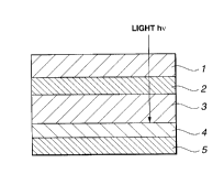
As a typical heterojunction structure of the present invention, it is
preferably of
such a structure in which a light-transmitting electrode 2, such as ITO
(indium tin
oxide) comprised of a transparent substrate 1 of silicon or glass, an
electrically
conductive high polymer film 3 of e.g., polythiophene, a fullerene polymer
film 4
forming a heterojunction with the electrically conductive high polymer film,
and a
counter-electrode 5 of, for example, aluminum, are layered in this order on
the
28
CA 02312140 2000-06-22
transparent substrate 1, as shown in Fig.33A. An active layer 6 of, for
example,
carbon nanotube or phthalocyanine, is preferably interposed as a carrier
generating
layer between the electrically conductive high polymer film 3 and the
fullerene
polymer film 4, as shown in Fig.33B. The film thicknesses of the electrically
conductive high polymer film 3, active layer 6 and the fullerene polymer film
4 are
preferably 0.1 to 50 nm and more preferably 5 to 20 nm, hereinafter the same.
It is noted that charge separation is also possible in a heterojunction
structure
in which the electrically conductive high polymer film 3 and the fullerene
polymer film
4 are interchanged with each other, as shown in Figs.34C and 34D, such that
this
structure is also comprised in the scope of the present invention.
The electrically conductive organic film is electron-donating and is
preferably
comprised of p-type electrically conductive high molecular material containing
a
covalent ~-electron system. Preferred examples of the polymers include those
of
polyvinyl carbazole, poly (p-phenylene)- vinylene, polyaniline, polyethylene
oxide,
polyvinyl pyridine, polyvinyl alcohol, polythiophene, polyfluorene,
polyparaphenylene
and derivatives of these constituent monomers.
Meanwhile, these electrically conductive organic films may be admixed with
known dopants, such as sulfuric acid radicals, for controlling their
electrically
conductivity.
The fullerene polymer film operates as an electron accepting thin film and
preferably composed of a C6o polymer and/or C~~ polymer, such as those shown
for
29
CA 02312140 2000-06-22
example in Figs.S to 11, in Figs.l3 to 32 and in Figs.3 and 4. However, the
polymers
are not limited to these examples. In comparison with the vapor-deposited
fullerene
film, shown in Fig.2, this fullerene polymer film features tight bonding among
fullerene molecules by covalent bonds.
The active layer, as an optionally provided layer, is a carrier generating
layer,
and is formed of dyes having a Tc-electron system, metal complexes,
electrically
conductive high polymer materials, fullerene molecules, chemically modified
derivatives thereof, single- or multi-layered carbon nanotubes, either alone
or in
combination. The dyes may be enumerated by cyanine dyes, phthalocyanine, metal
complexes thereof, porphyrin and metal complexes thereof. As the material of
the
light-transmitting electrode, the ITO (indium oxides doped with tin) is
generally
preferred. However, thin films of gold, silver, platinum or nickel may also be
used.
The materials of the counter-electrode may be enumerated by one or more of
metals, such as aluminum, magnesium, indium, alloys thereof, or ITO.
The manufacturing method of the present invention for producing the charge
separation heterojunction structure basically includes a step of forming a
light-
transmitting electrode, a step of forming an electrically conductive organic
film, a step
of forming a fullerene polymer film and a step of forming a counter-electrode.
The
sequence of these steps is, however, arbitrary, on the condition that the
fullerene
polymer film is to be identified first before proceeding to the formation of
the
remaining constituent layers. The step of mounting a substrate on the light-
CA 02312140 2000-06-22
transmitting electrode or the counter-electrode or the step of interposing an
active
layer may be added as appropriate.
For this identification, the Raman method and the Nexafs method, both being
non-destructive spectroscopic method, are preferably used in combination. If
one of
these methods is omitted, the identification cannot be executed
satisfactorily.
Among items of evaluation of the specified identification operations, there
are
a fullerene polymer structure, polymerization degree, amorphization, oxidation
and
insulation destruction by impression of a high voltage. The results of the
evaluation
may be used not only for identification of the fullerene polymer film but also
for
controlling physical properties, such as control of polymerization conditions.
In the step of forming the light-transmitting electrode, the routine practice
is
forming the electrode on a substrate, rather than forming it alone. The
electrode
material, such as ITO, is formed on the substrate by techniques such as vapor
deposition or sputtering.
If thin film of a stable metal, such as gold, is used in place of ITO film, it
is
crucial to form the thin film to a thin thickness on the substrate to provide
light
transmittance. The shape or the pattern of the light-transmitting electrode
may be
freely selected by known means, such as mask.
The electrically conductive organic film or the fullerene polymer film is
formed
on the light transmitting electrode. Meanwhile, in case the fullerene polymer
film is
formed on the light-transmitting electrode, the procedure may be simply
reversed from
31
CA 02312140 2000-06-22
that employing the electrically conductive organic film, the corresponding
explanation
is omitted for simplicity.
During this forming step, a vapor-deposited film or a plasma polymerization
film of an organic low molecular compound, exhibiting electron donating
properties,
is formed on the light-transmitting electrode.
That is, if a monomer of the high molecular material or an organic low
molecular compound containing ~-electrons is vaporized and the gas thus
yielded is
irradiated with a high frequency plasma of a lower energy, UV rays or an
electron
beam, an electrically conductive organic film can be produced on the light-
transmitting
electrode.
The vapor-deposited film or the plasma polymerization film of the ~t-covalent
organic low molecular material has electrically conductivity at least of the
order of 109
S/cm. Since the fullerene polymer film, as later explained, operates as an
electron
accepting thin film, the low molecular organic vapor-deposited film or the
plasma
polymerization film needs to operate as an electron donating thin film.
The low molecular organic compounds may be enumerated by a ~ covalent low
molecular material, such as ethylene or acetylene, cata-condensation organic
compounds, such as benzene, naphthalene or anthracene, peri-condensation
aromatic
compounds, such as perillene or coronene, and derivatives of these compounds
as to
hetero atoms, such as nitrogen, oxygen or sulfur. It is noted that oxygen,
sulfur,
selenium or tellurium can be built as hetero atom into an organic skeleton,
however,
32
CA 02312140 2000-06-22
since these atoms normally furnish two electrons to the ~-electron system,
there are
furane or thiophene as a hetero cyclic compound of oxygen or sulfur which
proves a
~-electron system with e.g., benzene. If one of these elements is built into a
six-
membered ring or two of the elements are built into a five-membered ring, the
~-
electron system is present in excess amount in view of the 4n+2 rule so that
the
resulting compound is strongly electron-donating. Typical of the strong
electron-
donating compounds is tetrathiafullvalene. The vapor-deposited film or the
plasma
polymerization film of this strongly electro-donating organic compound forms a
heterojunction with an electron-accepting fullerene polymer film as later
explained to
induce charge separation by light induction more effectively.
The materials for forming the electrically conductive organic film, as
polymers,
may be enumerated by high molecular materials or derivatives thereof, in
addition to
the above-mentioned polyvinyl carbazole and polythiophene, these may being
used
alone or in combination.
These materials are poly (3-alkylthiophene), poly [2-methoxy-5-(2'-
ethylhexoxi)
-p-phenylene)-vinylene, poly [2-methoxy-5-(2'-ethylhexoxi)-1,4-paraphenylene
vinylene, poly (3-alkylthiophene), poly (9, 9-dialkylfluorene),
polyparaphenylene, poly
(2, 5- diheptiloxy-1, 4- phenylene), polyphenylene, polyaniline, poly (p-
phenylene),
polyethylene oxide, poly (2-vinyl pyridine and polyvinyl alcohol). It is also
possible
to execute polymerization by illumination of a high frequency plasma of a
lower
energy, or UV-rays, X-rays or electron rays, in a gaseous atmosphere of these
high
33
CA 02312140 2000-06-22
molecular compounds or an organic compound containing the ~t-electron system,
to
produce a highly electrically conductive organic thin film.
On the electrically conductive organic film, produced as described above, a
fullerene polymer film is formed by the following procedure.
First, the fullerene molecules, as a starting material, those of C~,~,, C~~,
and
higher-order fullerene may be used, either singly or in combination. Most
preferred are
the CG~, fullerene, the Coo fullerene or mixtures thereof. In addition, the
fullerene of
higher orders, such as C~~, C~g, Cg~, C~~, C~4 and so forth may be contained
therein.
These fullerene molecules may be manufactured by an arc discharge method of
a carbon electrode, using an apparatus shown for example in Fig.35.
In a reaction vessel 8 of the present apparatus, there are mounted a pair of
carbon electrodes, connected to an AC or DC source 9, such as counter-
electrodes 10a,
10b formed of graphite. After evacuating the reaction vessel 8 by a vacuum
pump
through an outlet 11b by an exhaust pump, low-pressure inert gas, such as
helium or
argon, is introduced via an inlet 11a so as to be charged into the reaction
vessel 8.
The ends of the counter-electrodes 10a,10b are arranged facing each other with
a small gap in-between, and a predetermined current and voltage are applied
from the
DC source 9 to maintain the state of arc discharge across the ends of the
counter-
electrodes 10a, 10b for a predetermined time.
By this arc discharge, the counter-electrodes 10a,10b are vaporized so that
soot
is gradually deposited on a substrate 12 mounted on the inner wall surface of
the
34
CA 02312140 2000-06-22
reaction vessel 8. If this amount of soot deposited is increased, the reaction
vessel 8
is cooled and the substrate 12 is taken out, or the soot is recovered using a
sweeper.
From this soot, the fullerene such as C~,~, or C~~, may be extracted using a ~-
electron based solvent, such as toluene, benzene or carbon disulfide. The
yielded
fullerene, obtained in this stage, is termed crude fullerene, which may be
applied to
column chromatography to separate C~,~ and C~~, as purified separate products.
The resulting fullerene molecules are used as a starting material in the film-
forming process of the fullerene polymer. Among the polymerization or film-
forming
methods, there are, for example, a photopolymerization method, an electron
beam
illumination method, a plasma polymerization method, a micro-wave
polymerization
method) and an electrolytic polymerization method.
Photo Polymerization Method
In this polymerization method, an apparatus including a reaction chamber
capable of being maintained at a reduced pressure or in vacuum, heating means,
such
as resistance heating means, for vaporizing the fullerene molecules, and
illumination
means for illuminating the light, such as ultraviolet beam, through the window
of the
reaction chamber, is used. A fullerene polymer film is formed on the substrate
as
fullerene is evaporated and illumination of ultraviolet light is continued for
a
predetermined time. At this time, the fullerene molecules are excited by light
and
polymerized through the excited state.
It is noted that polymerization occurs by forming an evaporated film and
CA 02312140 2000-06-22
illuminating ultraviolet rays thereon, without illuminating the light as the
evaporation
is going on. In this case, there are occasions wherein only a superficial
layer of the
film is polymerized, whilst the bulk part of the film is not polymerized. An
experiment
conducted by the present inventors have revealed that a pattern of cracks can
be
produced on the surface of the evaporated fullerene film on UV irradiation, as
may be
observed over a microscope.
Electron Beam Polymerization Method
This method uses an electron beam radiated from the electron gun in place of
the light such as ultraviolet light. The principle of polymerization is
similar to the
photo polymerization method, that is, the fullerene molecules are excited by
an
electron beam and polymerized through the excited state.
Plasma Polymerization Method
Among the plasma polymerization methods, there are a high-frequency plasma
method, a DC plasma method and an ECR plasma method. Here, the high-frequency
plasma method, which is now in widespread use, is explained by referring to
the
drawings.
Fig.36 shows a typical high-frequency plasma polymerization apparatus,
including a vacuum vessel 13, within which are arranged a pair of electrodes
14a, 14b
facing each other. These electrodes are connected to an outer high frequency
power
source 15. On one 14b of the electrodes is set a substrate 16 for permitting a
fullerene
polymer film to be deposited thereon, that is the above-mentioned substrate
having the
36
CA 02312140 2000-06-22
electrically conductive high polymer film formed on the light-transmitting
electrode.
In this vacuum vessel 13, there is arranged a vessel 17 formed e.g., by a
molybdenum boat, accommodating the fullerene molecules, as a starting
material.
This vessel 17 is connected to an external power source for resistance heating
18.
In the polymerization apparatus, constructed as described above, a low-
pressure
inert gas, such as argon, is introduced through an inlet 19 into the vacuum
vessel 13,
which is evacuated through the exhaust port 20. After the vacuum vessel 13 is
charged
with the inert gas, the current is supplied to the vessel 17 to heat it to
vaporize the
fullerene molecules therein. The high frequency voltage is applied from the
high
frequency power source 15 to generate a high frequency plasma across the
electrodes,
while illumination is made into the fullerene gas to form a fullerene polymer
film
holding the ~-electron skeleton on the substrate 16.
Meanwhile, a DC power source may be used in place of the high frequency
power source 15 (DC plasma method). If the vessel 17 is heated without
actuating
these power sources, that is without generating the plasma, the fullerene is
not
polymerized, with its evaporated film being formed on the substrate 16.
If the temperature of the substrate 16 is excessively high, the amount of
deposition of the fullerene polymer film is decreased. Therefore, the
substrate is
usually kept at a temperature of 300° C or less. If the plasma power is
of the order of
100 W, the temperature scarcely exceeds 70°C.
37
CA 02312140 2000-06-22
Microwave Polymerization Method
Fig.37 shows a typical microwave polymerization apparatus including a vessel
21, such as a molybdenum boat, accommodating the fullerene molecules as a
supply
source of a starting material, a microwave operating portion 23 for causing
the
microwave 22 to operate on flying fullerene molecules, a reaction chamber 25
for
generating a fullerene polymer by induction by the microwave 22 (excitation of
asymmetric plasma) and for forming its film on the gas 24, and a microwave
generating device for generating the microwave 22.
In an inner wall of the polymerization apparatus in the vicinity of the vessel
21
is opened a gas inlet tube 26 for introducing a carrier gas, such as an argon
gas, into
the inside of the apparatus. This carrier gas 27 has not only the capability
of entraining
fullerene molecules 27 to bring them onto the substrate 24 in the reaction
chamber 25
but the capability of modifying the surface of the substrate 24 in the
following manner.
That is, if, before introducing the fullerene molecules 28 into the inside of
the
apparatus, the carrier gas 27 is introduced and excited by the microwave
operating
portion 23 so as to be bombarded onto the surface of the substrate 24 in the
reaction
chamber 25, the substrate surface is etched by the excited carrier gas 27 to
improve
adhesion of the substrate surface with the fullerene polymer film deposited
thereon.
The microwave generating device (microwave unit) includes a microwave
oscillation source 29, an isolator 30, a power meter 31, a three-stub tuner 32
and a
reflection cavity 34, interconnected by a wave guide tube 35. Of these, the
microwave
38
CA 02312140 2000-06-22
oscillation source 29 is made up of an oscillation source, such as a
magnetron, whilst
the isolator 30 and the power meter 31 have the functions of rectifying the
microwave
and of detecting the microwave power. The three-stub tuner 32 is a device for
adjusting the number of oscillations of the microwave, having the function of
matching
the number of oscillations, whilst the reflection cavity 34 is a device for
reflecting the
microwave and matching the wavelength to convert the microwave in the
microwave
operating portion 23 into a standing wave.
The reaction chamber 25 may be larger in diameter than a resonant tube 36
which is a flow duct of the carrier gas 27 and the fullerene molecules 28, and
is
configured so that the fullerene molecules induced efficiently to high density
in the
microwave operating portion 23 of the resonant tube will be led onto a
substrate 24 of
e.g., silicon, provided on a support, not shown, where the fullerene polymer
film will
be formed uniformly. In the reaction chamber 25, there is provided an
evacuating
system 37 for maintaining a pre-set pressure in the reaction chamber 25.
The support for mounting the substrate 24 thereon may be electrically
conductive or insulating. It may also be provided with heating means, such as
current
supplying means.
If this microwave polymerization device is to be used, the inside of the
reaction
chamber 25 is maintained at a pressure of approximately 0.05 to 1 Torr, with
e.g., an
argon gas, whilst the vessel 21 is heated by heating means, not shown, for
vaporizing
the fullerene molecules therein. The vaporized fullerene molecules then are
39
CA 02312140 2000-06-22
illuminated with e.g., a high frequency plasma of the order of 13.56 MHz by
the
microwave operating portion 23. This excites the fullerene molecules to form a
fullerene polymer film on the substrate 24.
The temperature of the substrate 24 of 300° C or less usually suffices.
If this
temperature exceeds 300°C, the amount of deposition of the fullerene
polymer film
is occasionally lowered. It is noted however that deposition of the fullerene
polymer
film is facilitated by applying a bias voltage. No special control is needed
to maintain
the substrate temperature in the above range during film formation. For
example, if the
microwave power is of the order of 100 W, the temperature rarely exceeds
100°C.
Meanwhile, if the substrate 24 is put on the microwave operating portion 23,
the tel
is occasionally increased to near 1000°C.
Method of Illuminating the Evaporated Film with Electromagnetic Wave
In this method, a vapor-deposited film 4A of fullerene molecules, such as
those
of C~~, is formed on the substrate 1, as shown in Fig.38A. During this vapor
deposition, the film thickness of the vapor-deposited film 4A is measured to
control
the film thickness to e.g., 10 A (thickness of a single molecule) to 200 nm to
execute
vapor deposition. After forming the vapor-deposited film to a pre-set film
thickness,
the vapor-deposited film 4A is polymerized by illumination of the
electromagnetic
waves 10, such as RF plasma, as shown in Fig.38B, to form the fullerene
polymer film
4. The above-mentioned film thickness can be measured using a film thickness
meter
11 arranged in vacuum chamber 13, as shown in Fig. 39.
CA 02312140 2000-06-22
Fig.8 shows an evaporation device including a susceptor 12 arranged in the
vacuum vessel 13. On the susceptor 12 is set a substrate on which to deposit
an
evaporated fullerene film. This substrate may, for example, be a substrate 1
on which
the fullerene polymer film is to be deposited, that is the substrate on which
the
electrically conductive high molecular film has been formed on a light-
transmitting
electrode.
In the vacuum vessel 13 is arranged a vessel 17, such as a molybdenum boat,
for accommodating fullerene molecules as a starting material therein. This
vessel is
connected to an external resistance heating power sourcel8.
In the evaporation device, constructed as described above, the current is
supplied to the vessel 17 in the evacuated vacuum vessel 13, to heat the
vessel to
vaporize the fullerene molecules therein to form an evaporated fullerene film
of
fullerene 4A on the substrate 1.
Then, in a high frequency plasma polymerization apparatus of Fig.40, in which
a pair of electrodes 14a, 14b are arranged facing each other in a vacuum
vessel 23 and
are connected to an external high frequency power source 15, the substrate 1,
carrying
the evaporated fullerene film 4A, is set on the electrode 14b.
In this polymerization apparatus, a low pressure inert gas, such as argon, is
supplied into the vacuum vessel 23, evacuated through the exhaust port 20, to
fill the
inside of the vacuum vessel 23 with the gas. The high frequency voltage is
applied
from the high frequency power source 15 to generate a high frequency plasma
across
41
CA 02312140 2000-06-22
the electrodes 14a and 14b, at the same time as the evaporated fullerene film
4A is
illuminated and thereby polymerized to form a fullerene polymer film 4 having
the ~-
electronic skeleton.
The high frequency power source 15 may be replaced by a DC power source
(direct current plasma method). If the devices of Figs.8 and 40 are combined
as shown
in Fig.38, and the vessel 17 is heated without driving the power source 15,
that is
without generating the plasma, the evaporated fullerene film 4A is formed on
the
substrate 1. The power source 15 may be driven in the same apparatus to effect
polymerization in a manner as described above.
The fullerene molecules may be C«, or C.,~, either alone or as a mixture. As
the
electromagnetic waves, an RF plasma, UV rays or an electron ray may be used.
Electrolytic Polymerization Method
Fig.41 shows a typical electrolytic polymerization apparatus in which an
electrode 39 as a positive electrode and an electrode 40 as a negative
electrode, both
connected to a potentiostat 41, are provided in an electrolytic cell 38, and
in which a
reference electrode 42 is connected to the same potentiostat 41 so that a pre-
set
electric potential is applied across the electrodes 39 and 40.
The electrolytic cell 38 is provided with a gas inlet tube 45 for introducing
the
inert gas 44 for removing an oxygen gas etc from a non-aqueous solvent 43. In
a
lower portion of the electrolytic cell 38, there is provided a magnetic
stirrer 46 for
causing movement of a stirrer, not shown, provided in the cell.
42
CA 02312140 2000-06-22
For operating the electrolytic polymerization apparatus, constructed as
described above, fullerene molecules, as starting material, a supporting
electrolyte, for
accelerating electrolysis, and the non-aqueous solvent 43, are charged into
the
electrolytic cell 38 and the potentiostat 41 is operated to cause a pre-set
electrical
energy to operate across the electrodes 39, 40. Then, a majority of the
fullerene
molecules are turned into anionic radicals, whilst a fullerene polymer is
formed as a
precipitate as a thin film and/or a precipitate on the negative electrode 40.
Meanwhile,
the spherically-shaped fullerene polymer, obtained as a precipitate, can be
readily
recovered by filtration or drying. After recovery, the polymer can be
solidified or
kneaded into a resin to form a thin film.
Although the electrodes 39, 40 are preferably metal electrodes, they may also
be formed of other electrically conductive materials, or by vapor depositing
metal or
other electrically conductive materials on a silicon or glass substrate. The
materials
of the reference electrode 42 need not be limited to particular metals,
depending on the
sort of the supporting electrolyte.
The removal of e.g., oxygen by the inert gas 44 may usually be helium gas
bubbling. The helium gas may also be replaced by other inert gases, such as
nitrogen
or argon. For completely removing oxygen etc, it is advisable to dehydrate the
non-
aqueous solvent, composed of first and second solvents, as later explained,
using a
dehydrating agent, to evacuate the solvent, to save the respective solvents in
ampoules
and to introduce the solvents saved in the ampoules through a vacuum line into
the
43
CA 02312140 2000-06-22
electrolytic cell 38.
It should be noted that oxygen etc is removed from the electrolytic solution
in
order to prevent oxygen etc from being captured into the fullerene polymer
film to
suppress paramagnetic centers to improve stability of the fullerene polymer
film.
As the supporting electrolyte, tetrabutyl ammonium perchloride, lithium
tetrafluoro borate (LiBF4), lithium hexafluoro phosphate (LiPF~,), sodium
peroxide
(NaC104), LiCF3S03, and lithium hexafluoro arsenide (LiAsF~,) may be used. If
these
supporting electrolytes are used, the produced spherical carbon polymers tend
to be
precipitated in the electrolytic solution.
If lithium perchloride (LiC104) or tert-butyl ammonium perchlorate is used, a
spherically-shaped carbon polymer can be produced as a thin film on the
electrode,
depending on the temperature at the time of the electrolytic polymerization
reaction.
According to the present invention, a mixed solvent composed of a first
solvent,
capable of dissolving fullerene molecules, and a second solvent, capable of
dissolving
the supporting electrolyte, is preferably employed. The mixing ratio of the
first
solvent to the second solvent is preferably 1:10 to 10:1 in volume ratio.
The first solvent is preferably a solvent of lower polarity, having a ~-
electronic
system (low polarity solvent). Examples of this sort of the solvent include
one or more
selected from the group of carbon disulfide (CS2), toluene, benzene and o-
dichlorobenzene.
The second solvent is preferably an organic solvent having a high dielectric
44
CA 02312140 2000-06-22
constant, such as, for example, acetonitrile, dimethyl formamide, dimethyl
sulfoxide
and dimethyl acetoamide. Of these, acetonitrile is most preferred.
In general, the fullerene molecules are dissolved only in low-polar solvent,
such
as carbon disulfide, while being extremely low in solubility even in aliphatic
solvents,
such as n-hexane. This is the most serious problem in electrolytic
polymerization of
the fullerene molecules.
The reason is that the supporting electrolyte used in electrolytic
polymerization
is dissolved only in polar solvents, such as water.
In carrying out electrolytic polymerization of the fullerene molecules, it is
necessary to use such a solvent as is capable of dissolving both the fullerene
molecules
and the supporting electrolyte. However, there lacks a single solvent
satisfying this
condition. At least a mixed solvent made up of individual solvents having the
above-
mentioned dissolving properties needs to be used.
However, mixed solvents satisfying these conditions may not unconditionally
be used. If such mixed solvent simply is used, it is a frequent occurrence
that the
solvent is insufficient in solubility for the fullerene molecules and/or the
supporting
electrolyte.
For example, an aqueous solvent, including water, is known to be an optimum
solvent for the supporting electrolyte which is a salt. However, it is only
insufficiently
soluble in the low-polar solvent capable of dissolving fullerene molecules.
Therefore,
the mixed solvent composed of the two solvents cannot be said to be optimum.
CA 02312140 2000-06-22
Our researches have revealed that the desirable mixed solvent used in the
present invention is made up of the first and second solvents, with the first
solvent
being a low polar solvent and the second solvent being an organic solvent of
high
polarity and large dielectric constant.
Among the above-specified second solvents, acetonitrile, a solvent frequently
used in preparing radicals of an organic matter in the presence of a
supporting
electrolyte in an electronic cell, is most preferred.
It is however unnecessary to use this acetonitrile as the second solvent in
limiting manner since dimethyl formamide or other organic solvents are also
desirably
used in the present invention.
The fullerene polymer film, produced as described above, is formed on a
silicon
or glass substrate, a transparent electrically conductive substrate of, for
example, ITO,
or on a metal substrate of gold, platinum or aluminum formed by vapor
deposition or
sputtering on a substrate of silicon or glass. There are occasions wherein the
fullerene
polymer film is formed on a so-called comb-shaped electrode obtained on vapor
deposition or sputtering of gold, platinum or aluminum using a mask, or
wherein the
fullerene polymer film is sandwiched between two electrodes. For producing
such
structure, it suffices if a fullerene polymer film is formed to a desired
thickness on a
metal electrode formed on a glass or silicon substrate or on a transparent
electrode
formed e.g., of ITO, a mask is placed on the fullerene polymer film and a
layer of
metals such a gold, platinum or aluminum, or a transparent electrically
conductive
46
CA 02312140 2000-06-22
layer of, for example, ITO, is formed thereon by e.g., sputtering or vapor
deposition.
On the surface of the fullerene polymer film, obtained by the above-mentioned
different polymerization methods, partial fullerene molecular structures are
left, so that
there exist numerous bonds of the double bond. Therefore, surface modification
(surface processing) in a variety of ways is possible.
For example, the fullerene polymer film can be surface-modified, using
techniques such as microwave induction, DC plasma or AC plasma, in an
atmosphere
of a hydrocarbon gas, such as acetylene, methane, ethane, propane, toluene,
benzene,
acetone, acetonitrile, ethanol or methanol, or a gas, such as oxygen,
hydrogen, chlorine
or fluorine. Alternatively, the fullerene polymer film may be surface-modified
in a
solvent using metal complex compounds or organic radicals.
This surface modification is effective to modify the fullerene polymer film or
to afford specificity thereto depending on the objective or application.
Meanwhile, the fullerene polymer film, in particular the fullerene polymer
film
obtained by the microwave polymerization method, suffers the problem of
dangling
spin. If, for example, microwave polymerization is carried out at ambient
temperature
with a power of from 100W to hundreds of W, using Coo and/or Coo as a starting
material, there is produced a fullerene polymer film containing approximately
10'g
spins/g of dangling spin.
This dangling spin significantly affects the electrically conductivity of the
fullerene polymer film, band structure or chronological stability of the
physical
47
CA 02312140 2000-06-22
properties.
This dangling spin is possibly produced by the fact that no ideal cross-linked
structure has not been formed. The amount of the dangling spin can be reduced
to
some extent by adjusting the substrate temperature for depositing the
fullerene
polymer film or by exposing the film to an atmosphere such as a hydrogen
plasma.
The process of decreasing the amount of the dangling spins may be confirmed
from
the difference in the absorption intensity by the electron spin resonance
method.
According to the present invention, a counter-electrode needs to be formed, as
an additional step, on a layered assembly comprising a light-transmitting
electrode -
electrically conductive high polymer film - fullerene polymer film or a light-
transmitting electrode-fullerene polymer film - electrically conductive high
polymer
film, obtained by the above respective steps.
This counter-electrode is formed of metals, such as aluminum, magnesium or
indium, or an alloy of two or more of these metals, in addition to oxides,
such as ITO,
and may be formed as a thin film on the fullerene polymer film by techniques
such as
vapor deposition, sputtering, electron guns or electrolytic plating.
In the heterojunction structure of the present invention, obtained in this
manner,
in which the electron-donating electrically conductive high molecular material
and an
electron-accepting fullerene polymer film are layered between the electrodes,
charge
separation may occur by light induction.
According to the present invention, it is crucial to identify the fullerene
polymer
48
CA 02312140 2000-06-22
film and to form the remaining structural layers subsequently during the step
of
forming each layer of the heterojunction structure.
That is, the information on the structure, polymerization degree,
amorphization,
oxidation and dielectric breakdown is obtained by spectroscopically analyzing
the
fullerene polymer film using in particular the Raman method and the Nexafs
method.
In general, the Raman spectrum is frequently used in the spectroscopic
analysis
of the carbon thin film. This method analyses the vibrations based on changes
in the
polarizability caused by irradiation of electromagnetic waves. This method is
used
frequently because the carbon material tends to absorb the IR rays to render
measurement difficult. As an example, Fig.43 shows the Raman spectrum of
amorphous carbon obtained with the CVD method at a lower temperature. An
excitation source is an argon ion laser at 514.5 nm.
The spectrum of Fig.43 reflects the features of the amorphous carbon film
sufficiently despite difference in line width. Two characteristics bands are
observed
in the vicinity of 1350 cm 1 and 1600 cm-1, these being termed a disorder band
and a
graphitic band, respectively.
If the fullerene polymer film is formed, and the above-described Raman
spectrum is produced, it may be estimated that changes have been produced in
the
amorphous carbon structure rather than the fullerene polymer. If a 1350 cm
band is
observed to a more or less extent, it may be premeditated that the
intermolecular cross-
linking structure is insufficient, or that there exist many dangling
structures.
49
CA 02312140 2000-06-22
In general, the Raman spectrum of the C~~, polymer having a periodic structure
is known to have many characteristic bands (see T. Wagberg et al., Appl. Phys.
A,
64,233 (1997), A.M. Rao et al., Phys. Rev. B. 55,4766 (1997)).
However, as for the Raman spectrum of a randomly interconnected polymer,
such as one obtained by the plasma polymerization method or the electrolytic
polymerization method, there has been given no definite standard for judgment.
On the other hand, the Nexafs spectrum observes transition from the core
electron (1s electron) of the carbon atom of the thin carbon film to the
unoccupied
orbitals and has so far been used for evaluating the unoccupied orbitals or
density of
the conducting band of an organic high molecular thin film.
The present inventors have found that more definite identification of the
fullerene polymer, which has so far not been possible, can be achieved only by
using
the Raman methos and the Nexafs method in combination.
The present invention will be explained more specifically in reference to
illustrative Examples which are not intended to limit the scope of the
invention.
Example 1 Measurement of Fermi level of the light-transmitting electrode (ITO
thin
film
An ITO thin film was formed by sputtering on a commercial quartz glass to
form a light-transmitting electrode and measurement was made of the PES
(photoelectron emission spectroscopy) to evaluate the Fermi surface level of
the ITO
thin film. The results are shown in Fig.44.
CA 02312140 2000-06-22
It was seen from the measured results that the Fermi level of the ITO thin
film
present at 4.87 eV below vacuum.
Example 2 Formation of polythiophene thin film (electrically conductive
organic film)
and measurement of physical properties thereof)
On this ITO film was then formed a commercial polythiophene thin film having
a sulfur radical as a dopant. The measured results of the PES of this
polythiophene thin
film are shown in Fig.45.
It was seen from the above results that the valence band edge level of the
polythiophene thin film exists at 4.82 eV below vacuum.
Moreover, a polythiophene thin film was also formed on the quartz glass and
measurement was made of the current-voltage characteristics thereof. Fig.46
shows the
measured results of the V-I characteristics and absorption coefficients by the
light
quantum energy.
A polythiophene thin film was formed on each of an ITO thin film and on a
metal film. First, the Fermi level of the ITO and gold was measured by the
photoelectron emission method and, based on the measured value, the Fermi
level of
the polythiophene thin film was measured by the contact potential method.
As a result, it was found that the Fermi level of the polythiophene thin film,
formed on the ITO thin film, was 4.4 eV, whereas that of the polythiophene
thin film,
formed on a gold thin film was 4.5 eV, which was close to 4.4 eV.
Example 3 (Formation of a fullerene polXmer film and measurement of various
51
CA 02312140 2000-06-22
physical~ro~,ertiesl
A fullerene polymer film then was formed on the above-mentioned
polythiophene thin film.
First, fullerene molecules, as a starting material, was prepared in the
following
manner. In an apparatus shown in Fig.35, arc discharge was effected by the 150
A
direct current in an atmosphere of 100 Torr of helium, using a graphite rod 35
cm in
length as a positive electrode. After fullerene was substantially vaporized to
produce
the fullerene containing soot, the polarities of the two electrodes were
reversed and
deposited heaped on the inherent negative electrode, such as carbon nanotubes,
were
further vaporized to produce the soot. The soot heaped in a water-cooled
reaction
vessel was recovered by a sweeper to produce crude fullerene by extraction
with
toluene. This crude fullerene was washed with hexane, dried and purified by
sublimation in vacuum. The fullerene molecules, thus produced, were subjected
to
time-of-flight mass spectrometry. It was thus found that the fullerene
molecules
contained C6o and C~~ at a rate of approximately 9:1.
Micro-Wave Polymerization
For forming a fullerene polymer film, fullerene molecules were charged into a
molybdenum boat and set on a site of a reaction tube of a micro-wave
polymerization
device shown in Fig.37. After evacuating the interior of the reaction chamber
by a
molecular turbo-pump, the argon gas started to be introduced. When the inside
of the
reaction chamber is constant at 0.05 Torr, a micro-wave oscillation device was
52
CA 02312140 2000-06-22
actuated to set a micro-wave power of 400 W by making adjustment by a tuner.
When
the micro-wave output is constant, current was supplied to the molybdenum boat
and
the current value was gradually raised to raise the temperature. Fullerene
vaporization
and heaping was monitored by a quartz film thickness sensor provided laterally
of a
substrate. For confirmation, the film thickness of the polymer film was
measured
using a contact type film thickness meter. For measuring the current, a
nanoammeter
was used. The band gap of the fullerene polymer film was determined from the
temperature dependency of the current value.
During film formation, a glass substrate and a silicon substrate etc were set
simultaneously in a bell jar to measure the physical properties. The mass
spectrography of the fullerene polymer film was effected by ionization and
ablation
by a pulsed nitrogen laser using a time-of-flight mass spectrometer. The
dangling
spins were measured using an x-band electronic spin resonation device in a
nitrogen
atmosphere. The number of dangling spins per unit weight of the fullerene
polymer
thin film was found by the relative comparison method of the third and fourth
absorption lines from the low magnetic field of a digital manganese marker,
using a
solution in toluene of d-tent-butyl nitroxide as a standard spin. The results
are as
follows:
film thickness (as measured with a contact film thickness meter): 30 nm
electrically conductivity: 1.1x10-$S/cm
band gap: 1.4 eV
53
CA 02312140 2000-06-22
dangling: 2.Ox10'8spins/g
wherein the value of the band gap is found from the results of measurement of
the transmittance by the forbidden-indirect method.
C60 then was purified, using a flush column charged with active charcoal
filler
in place of vacuum sublimation, and a fullerene polymer film was formed under
similar conditions. The results of the physical properties are as follows:
film thickness (as measured with a contact film thickness meter): 30 nm
electrically conductivity: 1.2x10-'S/cm
band gap: 1.5 eV
dangling: 2.Sx1018spins/g
Plasma Polymerization
In the foregoing, film forming is by micro-wave polymerization. Now, using an
RF plasma polymerization apparatus, shown in Fig.36, a fullerene polymer film
was
formed by an RF plasma (13.56 MHz) using the RF plasma polymerization device
shown in Fig.36. C60, as purified, was accommodated in a molybdenum boat and
vaporized by resistance heating to effect polymerization with a power of 70 W.
Similar evaluation of physical properties was conducted on the produced
fullerene
polymer film. The results are as follows:
film thickness (as measured with a contact film thickness meter): 30 nm
electrically conductivity: 1.8x10-'S/cm
band gap: 1.5 eV
54
CA 02312140 2000-06-22
dangling: 2.Ox10'xspins/g
Of the fullerene polymer films, obtained by the micro-wave polymerization
method, and by the plasma polymerization method, Raman spectroscopic
measurement
was conducted. It was suggested that the polymerization structures of the two
were
substantially the same.
The starting material then was switched from C~,~ to C~~, to perform Ar plasma
polymerization in the same was as described above. The results of evaluation
of the
physical properties of the produced fullerene polymer films are as shown
below:
film thickness (as measured with a contact film thickness meter): 45 nm
electrically conductivity: 1.0x10-xS/cm
band gap: 1.5 eV
dangling: 7.8x 10"spins/g
The results of Raman spectroscopic measurement of the Coo polymer film were
compared to those of the graphitic carbon. It was found that the so-called
disorder
band, as observed in the vicinity of 1350 cm' of the amorphous carbon, was not
observed. The 1460 and 1580 cm-1 bands were attributed to the symmetrical
extension/contraction vibrations of the single bond C-C and to the symmetrical
extension/contraction vibrations of the C=C double bond.
For clarifying the band structure of the fullerene thin film, the edge level
of the
valence band was evaluated from the photoelectron emission spectrum. The
results
are shown in Fig.48. For comparison, the results for the C6~ vapor-deposited
film are
CA 02312140 2000-06-22
also shown.
Method for vapor-deposited film electromagnetic wave illumination
In the present Example, a vapor-deposited C~,o polymer film was processed in
a Ar plasma into a C«, polymer.
(1) Formation of a fullerene polymer film
As a starting material, commercially available fullerene C~~, molecules were
used. These C~~ molecules can be produced as follows: using a known device,
arc
discharge was varied out by DC current of 150 A, under the atmosphere of 100
Torr
of helium, using a graphite rod 10 cm in diameter and 35 cm in length as a
positive
electrode. After the graphite rod was substantially vaporized to give a
fullerene
containing soot, the two electrodes were reversed in polarity and products
deposited
and heaped on the inherent negative electrode, such as carbon nanotubes, were
further
vaporized to produce the soot.
The soot heaped in a water-cooled reaction vessel was recovered to produce
crude fullerene by extraction with toluene. This crude fullerene was washed
with
hexane, dried and purified by sublimation in vacuum. The fullerene molecules,
thus
produced, were subjected to time-of-flight mass spectrometry. It was thus
found that
the fullerene molecules contained C~,o and C.,o at a rate of approximately
9:1.
Using the apparatus shown in Fig.39 or 36, the C~~ powders were sublimated
and vapor-deposited on a silicon substrate at 4x10⁻⁶ Torr to deposit a Coo
thin film,
controlled to a film thickness of 20 A, as measurement was made of the
thickness of
56
CA 02312140 2000-06-22
the vapor-deposited film by a film thickness meter. The C~,~ powders, set on
the
molybdenum boat, were heated gradually to approximately 600°C for
degassing and
was vapor-deposited at a higher temperature.
The vapor-deposited film was exposed to an Ar plasma of 0.1 Torr in an RF
reactor of plan-parallel plates started at 13.56 MHz. The C~,o thin film was
maintained
at 50°C and plasma processed for 4 hours and for 30 minutes at 30W and
50 W,
respectively, to a C~~ polymer film.
(2) XPS
Fig.49 shows the normalized XPS C lsspectra. The C 1s binding energies of
the evaporated C6o film and the plasma processed films were determined to be
284.9,
284.8 (30W) and 284.7 eV (50 W). The full width of half magnitude (FWHM) of
the
C 1s peak of the plasma processed films increased about 0.2 eV to 1.0 eV
compared
to that of 0.8 eV of the evaporated film. Moreover, the shape of the C 1s
becomes
asymmetric to higher binding energies. The calculated chemical shifts of the
C1s is
binding energy of +3 eV per four-membered ring in Coo polymers with respect to
the
isolated Coo molecule explains only partially the differences in the spectra.
On the
other hand, 13 (30W) and 15 at% (50 W) oxygen were found by XS. The rather
high
overall FWHM's (2.7 and 2.5 eV) measured for the O 1s peaks indicates that
different
molecular and atomic oxygen species are superimposed.
Fig.50shows the peak analyses of C 1s of the plasma processed films. Peaks
were found at 284.8 (284.7), 286.2 (286.1) and 288.7 (288.6) eV. The subpeaks
57
CA 02312140 2000-06-22
correlate to C-O, C-O-O and C=O added by structural changes.
Fig.51 illustrates the expanded region covering the C 1s shake-up satellites
(electron excitation). Five bands were separated by C~,~, by high-resolution
photoelectron spectroscopy at 1.8, 2.9, 3.7, 4.8 and 5.9 eV from the main peak
(approximately 285 eV). Three of these peaks were resolved for the evaporated
C~,o
film, but not the peaks at 2.9 and 4.8 eV. The observation of the shake-up
satellites
of the plasma processed films is somewhat problematic because they are
strongly
superimposed by the emission from oxidized carbon species.
Fig.52 shows the XS spectra of the evaporated C~~ film and the plasma
processed films. It is apparent that the plasma processed peaks become broader
and
reduced in intensity. In addition to the carbon states, the O 2s peak appears
at about
27 eV.
(3) TOF-MS
Figs.53 and 54 show the TOF-MS spectra of the plasma processed films. In the
spectra occur peaks in the mass range of about 1440, which are attributable to
fullerene polymer. Also, the C~~, structure is retained.
The results of Raman, XPS and TOF-MS confirm that the plasma processing
of evaporated C6~ films resulted in polymerized Coo. The described method
opens a
new route to polymerize Coo by plasma.
Example 4 Manufacture of hetero~unction structure and its physical properties
On the above-mentioned layered structure, including a polythiophene film and
58
CA 02312140 2000-06-22
a C60 polymer film, deposited on an ITO electrode, an aluminum electrode was
formed as a counter-electrode in the following manner. First, the inside of a
vapor
deposition device was evacuated to vacuum of 10-~ Torr by a turbo-pump and
subsequently back-filled with a high purity hydrogen gas. An aluminum film
then was
formed on the C~,o polymer film of the layered structure in a hydrogen
atmosphere of
10-5 Torr to produce a heterojunction structure.
From the evaluation of the valence electron band by the photoelectron emission
method, Fermi level by the contact potential difference method and the band
gap by
the optical technique, the band structure of the produced heterojunction
structure is
as shown in Fig.55.
The V-I characteristics of the heterojunction structure were evaluated. The
results are shown in Fig.56. Using a SOOW Xe lamp, it was checked whether or
not the
structure exhibited characteristics as a photocell. As a result, it was found
that, if light
is illuminated from the ITO side, an outstanding function as a photocell was
ascertained, as shown.
The V-I characteristics were evaluated on the heterojunction structure of the
same structure as described above except using gold in place of aluminum. The
results
are shown in Fig.57. This heterojunction structure has the function as the
photocell.
48.
For comparison, the relationship between the working temperature, current and
59
CA 02312140 2000-06-22
voltage was measured of a layered structure in which the polythiophene film is
omitted, indium and gold are used as a counter-electrode and in which an ITO
is used
as a light-transmitting electrode. The results are shown in Figs.58 and 59. It
may be
seen from these figures that desired V-I characteristics are not achieved such
that
characteristics are changed with temperature.
The Raman spectrum then was measured of the above-mentioned fullerene
polymer film.
Example 5
In the above plasma polymerization, the C6~, was plasma-polymerized using an
argon pressure of 0.1 Torr and a plasma power of 50 W. On measuring the Raman
spectrum of the produced polymer film, the spectrum as shown in Fig.60 was
obtained.
During this measurement, the power of the argon ion laser was suppressed to a
level
not causing changes in the light induction structure.
Example 6
The surface of the C~~, polymer film, obtained in the same way as in Example
5, was irradiated with a 200W argon plasma for two hours and Raman measurement
was conducted with the laser light of the same intensity as that used in
Example 5. As
a result, a Raman spectrum shown in Fig.61 was obtained.
Example 7
By the above-mentioned vapor deposition film electro-magnetic wave
illumination method, Raman measurement was conducted of the produced Coo
polymer
CA 02312140 2000-06-22
film with the laser light of the same intensity as that used in Example 5. As
a result,
the Raman spectrum shown in Fig.62 was obtained.
Example 8
A C~~, vapor-deposited film was formed as conventionally and Raman
measurement was conducted with the laser light of the same intensity as that
used in
Example 5. As a result, a Raman spectrum shown in Fig.63 was obtained.
Example 9
The Raman measurement was conducted on the commercially available
graphitic carbon. The results are shown in Fig.64.
The C60 molecule has ten active modes in the Raman spectrum. The strongest
line is seen at 1469 cm-', as shown in Fig.62. The distortion mode of the five-
membered ring of Ag(2) (C-C single bond expansion/contraction) is most
sensitive in
checking the state of polymerization. The spectrum shown in Fig.60
characterizes the
randomly oriented C~~ polymer. Specifically, the peak at 1464 cm' is
attributed to the
single-bond expansion/contraction vibration, whilst that at 1571 cm-' is
attributed to
the C-C symmetrical expansion/contraction vibration of the double bond. The
shoulder
present in the vicinity of 1425 cm' is attributed to the C-C symmetrical
expansion/contraction vibration of the intermolecular bond. Most crucial is
the fact
that the peak at 1470cm-' of the spectrum shown in Fig.63, termed the
pentagonal
pinch mode, is the source of the peak at 1464 cm-' of Fig.60, and is subjected
to slight
shifting.
61
CA 02312140 2000-06-22
The fact that a large disorder band can be seen on the spectrum of the Example
6 is indicative of amorphization. The spectrum of Example 6 coincides with
that of
Fig.64 as to the peak position of the graphitic carbon, despite the difference
in the line
width. That is, the profile of the spectrum such as that shown in Fig.60 is
peculiar to
that of the C~,o polymer.
Fig.65 shows the Raman spectrum of the C~,~ polymer film produced in an argon
plasma of 75 W and that of a C« polymer produced by the electrolytic
polymerization
method, as indicated in the treatise by the discoverers (P. Strasser, M.Ata,
J. Phys.
Chem. B, 102, 4131 (1998)). The two spectra coincide with the spectrum of
Fig.60
markedly as to the peak position and wave. With the Coo random oriented
polymer,
there are necessarily observed peaks at 1464 and 1571 cm-1.
Exampl a 10
The Raman spectrum was measured of the C« polymer films produced by the
plasma polymerization method for variable plasma powers under the pressure of
0.1
Torr. The results are shown in Fig.66.
The Raman spectrum was also measured of Coo polymer films produced by
varying the pressure under the SOW plasma power using a similar plasma
polymerization method. The results are shown in Fig.67.
Figs.68,69 and 70 show the results of Raman measurement of the Cbo vapor-
deposited films obtained by the vapor deposition method under the pressures of
0.01
Torr, 0.025 Torr and 0.2 Torr, respectively.
62
CA 02312140 2000-06-22
C60 polymer films were also formed by plasma polymerization at a pressure of
0.1 Torr and a plasma power of 10W and Raman measurement was carried out. The
results are shown in Fig.7l. The results of Raman measurement of C60 polymer
films,
obtained in similar manner except changing the plasma power to 30W, are shown
in
Fig.72.
The values of Raman shifting in the above measurements are collectively shown
in the following Table 3.
C~~, film forming pinch mode (cm-1) shift cm-1,
conditions compared to C60
SOW 0.01 Torr 1468.0 -1.0
0.025 Torr 1467.5 -1.5
0.05 Torr 1464.2 -4.8
0.1 Torr 1463.7 -5.3
0.15 Torr 1463.8 -5.2
0.2 Torr 1468.1 -0.9
0.3 Torr 1468.1 -0.9
0.1 Torr 10 W 1469.4 +0.4
30 W 1468.6 -0.4
50 W 1463.7 -5.3
Example 11
It is seen in Example 8 that the mode is shifted to a smaller number of waves,
several Raman lines are activated by disappearance of molecular symmetry, and
that
the C6o is polymerized as it holds its structure. This shifting is measured
for qualitative
and quantitative measurement of polymerization. The downward shift of 10 cm 1
may
theoretically be predicted as being ascribable to C6o dimers and trimers. By
the Raman
63
CA 02312140 2000-06-22
spectrum of the C~,~, thin film in the present example, the distortion mode of
the five-
membered ring of Ag(2) shifts by 4 to 5 cm' as compared to C~~.
The evaluation by the Nexafs method then was carried out.
Example 12
Measurement was made of a carbon K absorption edge Nexafs spectrum of a
C6~, vapor-deposited film. The results are shown in Fig.73.
Example 13
Measurement was made of a carbon K absorption edge Nexafs spectrum of a
C~,~ vapor-deposited film. The results are shown in Fig.74.
The transition portion to the ~ antibonding orbitals of Examples 11 and 12 is
shown enlarged in Fig.75. The attribution of inherent values derived from
calculations
of the molecular orbit on the semi-empirical level and calculations carried
out with
parameterization of both MNDO/AN-1 and MNDO/PM-3 are shown. The calculated
results of the C6~ dimers on the same level indicated that the spectral
intensity may be
predicted to occur with decrease in the number of electrons deemed to be n-
electrons
despite the occurrence of orbit level dispersion. The actual spectral pattern
reproduces
this satisfactorily.
Example 14
Nexafs measurement was conducted on the thin carbon film shown in Fig.6.
The results are shown in Fig.76, showing a pattern totally different from that
shown
in Examples 11 and 12, thus supporting the progress of amorphization.
64
CA 02312140 2000-06-22
Example 15
The surface of the sample of Example 13 was processed for five minutes with
SOW plasma and Nexafs measurement was conducted of the oxygen K-edge. The
results are shown in Fig.77. Since inherently the peak of this sort is not
observed on
a non-oxidized surface, it may be surmised that strong plasma illumination has
induced
amorphization, whilst oxidation has proceeded in atmosphere.
The above-described results of Nexafs measurement were compared on the
valence band level. The results are shown in the following table 4.
Table 4
film-forming condition valence band edge level (eV)
(polymerization
condition)
Coo vapor-deposited 6.25
film
SOW 0.01 Torr 5.22
plasma polymerization0.1 Torr 5.57
0.3 Torr 5.34
Fig.78 shows the relationship between the spectrum by the Nexafs method
described above and the orbit transition of electrons and holes due to light
induction
associated therewith.
Example 15
A heterojunction structure comprising an ITO electrode, manufactured in
Example 4, a polythiophene film, a Cb~, polymer film and an aluminum electrode
(counter-electrode), in which a phthalocyanine film (active layer) is
interposed
CA 02312140 2000-06-22
between the polythiophene film and the C~,~, polymer film and gold was used
for the
counter-electrode, was prepared by the method shown in Example 4.
The V-I characteristics of the heterojunction structure are shown in Fig.79,
from
which it is seen that the structure exhibits optimum photocell
characteristics. The
results of the photoelectron emission spectrum of the phthalocyanine film and
the
relationship between the photon energy and the absorption coefficient are
shown in
Figs.80 and 81, respectively.
Example 16
A heterojunction structure comprising an ITO electrode, manufactured in
Example 4, a polythiophene film, a C~,o polymer film and an aluminum electrode
(counter-electrode), in which a glass substrate is layered on an outer surface
of the
ITO electrode (surface exposed to atmosphere) in Fig.34C, was prepared by a
method
shown in Example 6.
This heterojunction structure failed to operate satisfactorily as a photocell.
However, the structure is usable for measuring e.g., the light volume because
it permits
charge separation and displays linear V-I characteristics.
Example 17
A heterojunction structure of Example 1S, in which aluminum was used as the
counter-electrode in place of gold, was prepared by the method shown in
Example 6,
and its VI characteristics were measured. The results are shown in Fig.82,
from which
it is seen that this heterojunction structure exhibits the function as the
photocell.
66
CA 02312140 2000-06-22
Example 18
First, tetrathiafulvalene molecules were deposited as a film on an ITO film
similar to that of Example 1, by illuminating an argon plasma of a low plasma
power
of 20 W, as the molecules were vaporized by a molybdenum resistance heater. In
the
same process, a thin film was also formed on a glass substrate to measure the
photoelectron emission and the band gap. As a result, the band gap was
evaluated to
be 2.4 eV, whilst the valence edge substantially coincided with the Fermi
level of ITO.
The measured results of Raman and IR of the produced tetrathiafullvalene
suggested that the tetrathiafulvalene molecules are of a dehydrogenated and
polymerized structure. The electrically conductivity was of the order of 10-4
to 10-2
S/cm, depending on delicate conditions of the plasma.
On this tetrathiafulvalene thin film was then formed a fullerene polymer film.
First, fullerene molecules, as a starting material, were prepared as follows:
In the
device shown in Fig.35, arc discharge was carried out by DC: current of 150 A,
under
the atmosphere of 100 Torr of helium, using a graphite rod 10 cm in diameter
and 35
cm in length as a positive electrode. After the graphite rod was substantially
vaporized
to give a fullerene containing soot, the two electrodes were reversed in
polarity and
products deposited and heaped on the inherent negative electrode, such as
carbon
nanotubes, were further vaporized to produce the soot. The soot heaped in a
water-
cooled reaction vessel was recovered by a sweeper to produce crude fullerene
by
67
CA 02312140 2000-06-22
extraction with toluene. This crude fullerene was washed with hexane, passed
through
a flush column charged with the activated charcoal to yield only C60, which
then was
purified by sublimation in vacuum.
Next, a fullerene polymer film was formed. The fullerene molecules, as a
starting material, were prepared as in the above-described Example. The
fullerene
molecules were charged into a molybdenum boat and set on a site of a reaction
tube
of a micro-wave polymerization device. After evacuating the interior of the
reaction
chamber by a molecular turbo-pump, the argon gas started to be introduced.
When the
inside of the reaction chamber was constant at 0.05 Torr, a micro-wave
oscillation
device was actuated to set a micro-wave power of 50 W by making adjustment by
a
tuner. When the micro-wave output was constant, current was supplied to the
molybdenum boat and the current value was gradually raised to raise the
temperature.
Fullerene vaporization and heaping was monitored by a quartz film thickness
sensor
provided laterally of a substrate. For confirmation, the film thickness of the
polymer
film was measured using a contact type film thickness meter. For measuring the
current, a nanoammeter was used. The band gap of the fullerene polymer film
was
determined from the temperature dependency of the current value.
During film formation, a glass substrate and a silicon substrate etc were set
simultaneously in a bell jar to measure the physical properties. The mass
spectrography of the fullerene polymer film was effected by ionization and
ablation
by a pulsed nitrogen laser using a time-of-flight mass spectrometer. The
dangling
68
CA 02312140 2000-06-22
spins were measured using an x-band electronic spin resonation device in a
nitrogen
atmosphere. The number of dangling spins per unit weight of the fullerene
polymer
thin film was found by the relative comparison method of the third and fourth
absorption lines from the low magnetic field of a digital manganese marker,
using a
solution in toluene of d-tent-butyl nitroxide as a standard spin. Meanwhile,
the value
of the band gap was found from the results of measurement of the transmittance
by the
forbidden-indirect method.
These measured results were the same as those of the Example 3. Moreover, the
results of Raman spectroscopic measurement of the Coo polymer film and
evaluation
of the edge level of the valence band were the same as those in Figs.47 and
48.
Measurements were also made of transmittance characteristics of the layered
structure
of the ITO-tetrafullvalene -Coo polymer. The results are shown in Fig.83.
An indium electrode was set as a counter-electrode on a layered structure
comprising a C~,~ polymer deposited by plasma polymerization on the
tetrathiafullvalene film (electrically conductive polymer). First, the inside
of a vapor
deposition device was evacuated to vacuum of 10-8 Torr by a turbo-pump and
subsequently back-filled with a high purity hydrogen gas. An indium film was
formed
on a hetero thin film in a hydrogen atmosphere of 10-5 Torr. From the
evaluation of
the valence electron band edge by the photoelectron emission method, Fermi
level by
the contact potential difference method and the band gap by the optical
technique, the
band structure of the produced heterojunction structure is similar to that
shown in
69
CA 02312140 2000-06-22
Fig.55.
The V-I characteristics of the heterojunction structure were evaluated. Using
a SOOW xenon lamp, it was checked whether or not the structure has
characteristics
as a photocell. As a result, a marked photocell function could be ascertained
when the
light is illuminated from the ITO side.
Example 19
Another heterojunction structure, which is the same as that described above
except using aluminum in place of indium, was prepared, and its V-I
characteristics
were measured. The results are shown in Fig.84, from which it is seen that
this
heterojunction structure displayed a function as the photocell.
Example 20
A heterojunction structure comprising an ITO electrode, a tetrafullvalene
layer,
a C60 polymer layer and an indium electrode, manufactured in Example 18, in
which
the tetrafullvalene layer and the C60 polymer layer were interchanged, was
prepared.
This heterojunction structure, displaying linear VI characteristics, failed to
operate
satisfactorily as a photocell, however, it allowed for charge separation.
Example 21 ~Va~or deposition film electro-magnetic wave illumination method,
preparation of a solar cell and its phXsical propert~iesl,
For preparing the structure shown in Fig.85, and for first depositing a
carbonaceous thin film, a film forming device shown in Fig.86 was prepared.
This film
forming device is made up of a simple type organic solvent gas bubbler 50, a
gas bomb
CA 02312140 2000-06-22
51 for supplying a carrier gas thereto, and a simple type electrical furnace
52 for
thermal decomposition of the organic solvent gas. A needle valve 53 for flow.
duct
adjustment is provided in each of the flow duct between the gas bomb 51 and
the
organic solvent gas bubbler 50 and the flow duct between the gas bomb 51 and
the
electrical furnace 52.
The electrical furnace 52 has a furnace core 30 mm in diameter and a heater
52b
within which a thermocouple 52d for connection to an external heater
temperature
controller 52 and a quartz substrate (glass substrate) 52, corresponding to
the substrate
1, directly above the controller 52c, for assuring correct film-forming
temperature of
the quartz substrate SOe. Meanwhile, a relay circuit for PID control was
operated in
unison for temperature control of the quartz substrate SOe. With the film-
forming
device, constructed as described above, is able to deposit a carbonaceous thin
film
with a temperature error less than 1 ° C.
The temperature of the electrical furnace 52 was set to 800 ° C.
After
introducing the quartz substrate 52e into the quartz tube 52b, an argon gas,
with a
purity of 99.999%, was introduced from a gas bomb 51 into the quartz tube 52b
to fill
the inside of the tube with the argon gas.
When the inside of the quartz tube 52b is completely the argon gas atmosphere,
and the temperature has reached 800°C, the toluene gas was started to
flow into the
inside of the quartz tube 52b through the organic solvent gas bubbler 50. The
flow
velocity of the toluene gas, introduced into the organic solvent gas bubbler
50, was
71
CA 02312140 2000-06-22
maintained at 50 ml/min.
After continuing gas bubbling for 30 minutes, only the argon gas was allowed
to flow into the quartz tube 52b, and the electrical furnace 52 was cooled
gradually.
After confirming that the electrical furnace 52 was cooled substantially to
room
temperature, the quartz substrate 52e was taken out of the quartz tube 52b. On
the
surface of the quartz substrate SOe was formed a thin carbon film presenting a
mirror
surface.
On the carbon thin film, a C« polymer film was formed, as explained in
connection with Example 1. The junction structure of the carbon thin film and
the
fullerene polymer film, thus fabricated, is a structure useful for isolating
the carrier
generated on light illumination, such that, if the structure is used in a
compound
structure of, for example, a glass substrate-ITO electrode- carbon thin film-
fullerene
thin film- aluminum electrode, it is particularly useful for a solar cell.
This structure
has desirable properties, as may be seen from Fig.87 showing V-I
characteristics on
light illumination thereon.
What is detrimental in this case is that the electrically conductivity of the
light-
transmitting electrode is impaired when forming a carbon thin film on a light-
transmitting electrode formed e.g., of ITO.
For avoiding this problem, a compound structure such as a glass substrate-
thin
gold electrode- thin carbon film- fullerene polymer film- aluminum electrode
is
preferably used. This compound structure operates as a solar cell , as may be
seen
72
CA 02312140 2000-06-22
from the I-V characteristics before and after light illumination. In order to
provide a
compound structure optimum for this application, it is necessary to scrutinize
into
variable factors, such as band gap of the carbon thin film, thickness of the
fullerene
thin film or the Fermi surface level of the electrode material.
As may be seen from the foregoing, the heterojunction structure of the present
invention permits charge separation by light induction and finds application
as a solar
cell or as a light emitting diode.
Moreover, as for identification of the fullerene polymer, positive results can
be
achieved by the combined use of the Raman and Nexafs methods. Since it is
possible
to check that the fullerene polymer film has positively been formed before
proceeding
to the subsequent step of forming the next upper layer film forming step, the
targeted
heterojunction can be prepared reliably. Moreover, if the polymerization
degree of the
fullerene polymer film is found to be insufficient, the information may be fed
back to
the polymerization step to control the fullerene polymerization conditions.
Meanwhile, the heterojunction structure of the present invention may be
variably designed as to its layered structure, insofar as the above-described
basic
structure is kept, such that, depending on the application, the respective
layers can be
divided into plural layers, or the film thicknesses of the respective layers
can be
designed optionally.
In the heterojunction structure of the present invention, in which the
electron-
donating electrically conductive organic film and the electron-accepting
fullerene
73
CA 02312140 2000-06-22
polymer film are layered between a pair of electrodes, at least one of which
is light
transmitting, such that the heterojunction structure permits charge separation
by light
induction and finds application in a solar cell or a light emitting diode.
If the heterojunction structure of the present invention is used in a solar
cell, the
resulting solar cell is more economical than a conventional silicon pn
junction solar
cell and is superior in lightness and flexibility. Moreover, the solar cell
employing the
heterojunction structure compares favorably with the conventional solar cell
in energy
conversion efficiency. In addition, with the solar cell employing the
heterojunction
structure, an excellent photoelectric conversion efficiency can be achieved
without
employing a sensitizer in contradistinction from a titania-based solar cell.
With the manufacturing method of the present invention, respective constituent
layers of the heterojunction structure can be formed without difficulties,
while the
fullerene polymer film can be identified reliably by combined use of the Raman
and
Nexafs methods. In addition, the evaluation of variable items, such as
structures of the
fullerene polymer films, polymerization degree, amorphization degree,
oxidation or
dielectric breakdown due to application of high voltages, can be executed
reliably non-
destructively, while the results of the evaluation can be utilized for
controlling the
conditions for fabricating the heterojunction structure and hence the physical
properties of the heterojunction structure.
According to the present invention, the vapor-deposited film of fullerene
molecules is first formed and subsequently polymerized by illumination of the
74
CA 02312140 2000-06-22
electromagnetic waves, desired vapor-deposited films can be formed at all
times by
measuring the thickness of the vapor-deposited film by a film thickness meter
and by
controlling the conditions for vapor deposition, such as vapor-deposited
temperature,
with the result that the film thickness of the fullerene polymer film by
illumination of
the electromagnetic waves can be easily and accurately controlled to realize
the desired
film thickness.
Moreover, since the fullerene polymer film is polymerized by irradiation of
the
electromagnetic waves as the structure of the fullerene molecules is kept, so
that a
fullerene polymer film having a neat structure with the unimpaired fullerene
molecule
structure can be produced. In addition, even if an organic film is present on
the
underlying layer, there is no risk of the underlying layer being damaged by
the vapor-
deposited film formed thereon, while the underlying layer can be protected
from
illumination of the electromagnetic waves due to the presence of the vapor-
deposited
film.