Note: Descriptions are shown in the official language in which they were submitted.
CA 02312516 2000-06-27
INFRARED TRANSCEIVER WITH ISOLATED ANALOG OUTPUT
Field of the Invention
The present invention relates to transceivers. In particular, the present
invention relates to
an infrared digital transceiver having an isolated analog output.
Background of the Invention
Conventional digital infrared (IR) transceivers provide only a digital output.
The receiver
component of the transceiver converts infrared optical pulses into discrete
electrical pulses for
downstream processing.
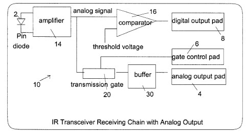
Figure 1 illustrates a conventional IR transceiver receiving chain. A
photodiode such as a PIN
1 o diode converts the optical energy from an infrared optical signal to an
electric current. The amplifier
converts the electric current to voltage and magnifies the voltage. The output
of the amplifier is fed
to a comparator input and a threshold voltage is applied to the other input of
the comparator. When
the analog output signal of the amplifier is greater than the threshold
voltage, the comparator emits
a digital pulse. If the analog signal amplitude is smaller than or equal to
the threshold voltage, the
~ 5 comparator output remains low. Thus the comparator hides small signal
information within the
analog profile of the optical signal output from the amplifier, including base
line voltage, noise
variance, system gain etc. These parameters are thus inaccessible and
untestable.
It is very difficult to apply digital signal processing (DSP) technology to IR
communication
in this conventional IR transceiver receiving chain. DSP is a very powerful
method of improving
2.0 communication quality, sensitivity and immunity, and the advantages of DSP
are well established
in other types of communication systems. However, DSP usually requires an
analog signal in order
to effect the analog to digital conversion, and a conventional IR transceiver
is incapable of providing
an analog signal without risking disruption of the operation of the receiver
chain.
Furthermore, the conventional IR transceiver is difficult to test and debug.
The analog
CA9-2000-0005
CA 02312516 2000-06-27
component of the receiver chain is the core of an IR transceiver, but because
the analog signal is not
accessible, when the device malfunctions or experiences product quality
problems common
diagnostic procedures are largely unavailable because the analog signal output
of the amplifier is
untestable.
It would therefore be advantageous to add an analog output to the receiver
chain in an IR
transceiver. However, since in an integrated circuit design the load
capability of an amplifier is
limited due to restrictions in the chip die size, this is significantly more
complex than merely adding
a connection from an analog output pad to the amplifier output. A direct
connection from the
amplifier output to an analog output pad would add an additional load on the
amplifier output which
would affect the receiver chain performance. The extra load results not only
from the parasitic
capacitance of the connection trace and the pad, but also from the input
impedance of external
components such as a DSP device or measurement instrument. If the additional
load is too heavy,
the IR transceiver performance will be degraded. In extreme cases, for example
where a large
capacitance is added to the amplifier output, a conventional IR transceiver
will oscillate and system
failure will result.
Summary of the Invention
The present invention overcomes these disadvantages by providing an IR
transceiver having
a receiver chain with an isolated analog output, and a method of implementing
an analog output in
an IR receiver chain.
2:o According to the invention, a transmission gate and unity gain buffer are
interposed between
the amplifier output and an analog output pad. The transmission gate behaves
as a switch, passing
the analog output signal to the analog output pad only when an analog output
is required. For
example, to use the analog output signal for digital signal processing, in the
case of a strong signal
it is unnecessary to use digital signal processing and the transmission gate
remains off. In the case
of a weak signal the transmission gate is turned on, passing the analog signal
to the unity gain buffer
which provides an analog signal output to the DSP device. The transmission
gate thus minimizes the
CA9-2000-0005
2
CA 02312516 2000-06-27
effect of the isolated analog output, and further serves as a switch and
multiplexer which allows a
single isolated analog output to be connected to different test points through
the use of multiple
transmission gates.
The unity gain buffer preferably has a high input resistance, a low input
capacitance, a unit
gain and a low output impedance. Thus, the load of the DSP device or measuring
instrument on the
analog output pad is isolated by the unity gain buffer and the transmission
gate, and does not affect
the performance of the receiver chain.
In the preferred embodiment the bandwidth of the transmission gate and the
buffer is wider
than that of the receiver chain, and since the transfer rate of the
transmission gate(when active) is
a unity and the transmission rate of the buffer is a unity, the analog output
pad provides an analog
signal substantially identical to the analog output of the amplifier.
The present invention thus provides an isolated analog output circuit for a
photoelectric
transceiver having a photodiode emitting a current proportional to an
intensity of an optical signal
to produce an analog electrical signal, the analog electrical signal being
amplified by a photodiode
15 signal amplifier to generate an analog input signal to the circuit, the
circuit comprising: a buffer
coupled to an analog output terminal, the buffer comprising a differential
amplifier having a very
high input impedance and substantially a unity gain, wherein when the analog
input signal is coupled
to an input of the differential amplifier, the buffer outputs an analog output
signal substantially
identical to the analog input signal while isolating the photodiode signal
amplifier from a load on
2:o the analog output terminal.
In a further aspect of the isolated analog output circuit, the differential
amplifier comprises
a first symmetrical transistor pair comprising an input transistor and an
output transistor having a
common current source or impedance for signal coupling and operating point
setting, the input and
output transistors passing a current in direct proportion to an amplitude of
an input voltage of the
25 input transistor, a second symmetrical transistor pair comprising a pair of
transistors, forming a
current mirror and an active load ofthe first symmetrical transistor pair,
connected between a voltage
CA9-2000-0005
CA 02312516 2000-06-27
supply and the first symmetrical transistor pair, and an output stage
comprising an output stage
transistor and a resistor forming an impedance transfer and feedback network
to the output transistor,
an input terminal of the output stage transistor being connected to an output
terminal of the first
symmetrical transistor pair and an output terminal of the output stage
transistor being connected to
ground through the output stage resistor and to an input terminal of the
output transistor of the first
symmetrical transistor pair and to the analog output terminal, wherein when
the analog input signal
is applied to the input terminal of the input transistor a current flows
through the input transistor and
the second symmetrical transistor pair raises the output terminal voltage of
the output transistor to
maintain substantially identical currents through the input transistor and the
output transistor, thereby
forcing a current through the output transistor to match the current through
the input transistor and
providing an output analog signal substantially identical to the input analog
signal.
The present invention further provides a photoelectric transceiver having a
photodiode
emitting a current proportional to an intensity of an optical signal to
produce an analog electrical
input signal, having an isolated analog output circuit comprising: a buffer
coupled to an analog
output terminal, the buffer comprising a differential amplifier having a very
high input impedance
and substantially a unity gain, wherein when the analog input signal is
coupled to an input of the
differential amplifier, the buffer outputs an analog output signal
substantially identical to the analog
input signal while isolating the photodiode signal amplifier from a load on
the analog output
terminal.
a:0 In a further aspect of the photoelectric transceiver, the differential
amplifier comprises a first
symmetrical transistor pair comprising an input transistor and an output
transistor having a common
current source or impedance for signal coupling and operating point setting,
the input and output
transistors passing a current in direct proportion to an amplitude of an input
voltage of the input
transistor, a second symmetrical transistor pair comprising a pair of
transistors, forming a current
2,5 mirror and an active load of the first symmetrical transistor pair,
connected between a voltage supply
and the first symmetrical transistor pair, and an output stage comprising an
output stage transistor
and a resistor forming an impedance transfer and feedback network to the
output transistor, an input
CA9-2000-0005
CA 02312516 2000-06-27
terminal of the output stage transistor being connected to an output terminal
of the first symmetrical
transistor pair and an output terminal of the output stage transistor being
connected to ground
through the output stage resistor and to an input terminal of the output
transistor of the first
symmetrical transistor pair and to the analog output terminal, wherein when
the analog input signal
is applied to an input terminal of the first symmetrical transistor pair a
current flows through the
input transistor and the second symmetrical transistor pair raises the output
terminal voltage of the
output transistor to maintain substantially identical currents through the
input transistor and the
output transistor, thereby forcing a current through the output transistor to
match the current through
the input transistor and providing an output analog signal substantially
identical to the input analog
signal.
In a further aspect of the invention a transmission gate for selectively
blocking or passing the
analog input signal to the buffer is provided. The transmission gate may
comprise at least one
transistor which selectively blocks or passes the analog input signal
responsive to a level of a gate
voltage, and in a preferred embodiment comprises a P-type FET and an N-type
FET with sources
~.5 (or drains) of the P-type FET and the N-type FET connected to the circuit
input and drains (or
sources) of the P-type FET and the N-type FET connected to an input of the
buffer, a gate of one of
the P-type FET and N-type FET being connected to a switching signal through an
inverter. Since the
source and drain of a P-type FET and an N-type FET are symmetrical and
exchangeable, the
connections of the sources and drains can be reversed without affecting the
operation of the
20 transmission gate.
In further aspects of the invention the input and output transistors of the
first symmetrical
transistor pair respectively comprise a pair of N-type FETs, a gate of the
input N-type FET being
connected to the analog input signal; the second symmetrical transistor pair
comprises a pair of P-
type FETs, the gates of the P-type FETs being connected to a drain of the
input N FET; the input and
2,5 output N-type FETs are grounded through a DC current source providing a DC
operating current to
the source coupled differential amplifier; and/or the output stage comprises
an N-type FET having
a source providing the analog output signal and a feedback voltage to a gate
of the output N-type
CA9-2000-0005
5
CA 02312516 2000-06-27
FET.
Brief Description of the Drawings
In drawings which illustrate by way of example only a preferred embodiment of
the
invention,
Figure 1 is a block diagram of a conventional infrared transceiver receiving
chain,
Figure 2 is a block diagram of an infrared transceiver receiving chain having
an isolated
analog output circuit according to the invention
Figure 3 is a schematic diagram of a preferred embodiment of the transmission
gate and
unity gain buffer in the receiving chain of Figure 2, and
1o Figure 4 is a schematic diagram showing a preferred embodiment of the unity
gain buffer
of Figure 3.
Detailed Description of the Invention
Figure 2 illustrates a receiver chain 10 in a photoelectric transceiver
according to the
invention. A photodiode such as a PIN diode 2 generates an electric current
proportional to the
optical energy of an infrared optical signal received by the PIN diode 2. A
conventional amplifier
14 converts the electric current to voltage and magnifies the voltage, which
is output to comparator
16. A reference voltage at a selected threshold level is applied to the
reference input of the
comparator 16. When the analog output signal of the amplifier 14 exceeds the
reference voltage, the
comparator 14 emits a digital pulse for the duration of the interval during
which the analog output
2o signal of the amplifier 14 exceeds the reference voltage, which is
transmitted to a digital device (not
shown) through digital output pad 8. At all other times the comparator output
remains zero.
According to the invention a transmission gate 20 and unity gain buffer 30 are
interposed
between the output of the amplifier 12 and an analog output pad 4 for
interfacing with an analog
CA9-2000-0005
6
CA 02312516 2000-06-27
device (not shown), which may be a DSP device, measurement or diagnostic
instrument, etc. The
transmission gate 20 and unity gain buffer 30 isolate the analog output pad 4
from the output of the
amplifier 12, thus substantially eliminating the effects of both the parasitic
capacitance of the analog
output pad 4 and the input impedance of the analog device.
Figure 3 illustrates a preferred embodiment of the transmission gate 20. The
transmission
gate 20, which is used in the case of weak analog input signals or analog
measurements, comprises
P-type FET 22 and N-type FET 24, with the sources of the P FET 22 and the N
FET 24 connected
to the transmission gate input and the drains of the P FET 22 and the N FET 24
connected to the
input of the buffer 30 (as noted above, these connections can be reversed
without affecting the
operation of the transmission gate). A control signal terminal SW controlled
by a gate control pad
6 is connected to the gate of the P FET 22 and to the input of an inverter 26,
the output of the
inverter 26 being connected to the gate of the N FET 24. The P FET 22 and N
FET 24 may both be
very small, in the order of 6 wm x 1.2 ~m (W x L), so when the transmission
gate 20 is turned off the
input capacitance to ground is lower than 6 fF and the leakage current is less
than 3 pA.
~.5 Thus, when the transmission gate control signal is in a high logic state
the logic state is high
at the gate of the P FET 22 and low at the gate of the N FET 24, both P FET 22
and N FET 24 are
turned off and the analog output signal from the amplifier 12 is blocked. When
the control signal is
in a low logic state the logic state is low at the gate of the P FET 22 and
high at the gate of the N
FET 24, both P FET 22 and N FET 24 are turned on, and the analog input signal
from the output of
20 the amplifier 12, which is connected to the sources of the FETs 22, 24, is
passed to the unity gain
buffer 30. The transmission gate 20 thus selectively passes the analog input
signal to the analog
output pad 4 responsive to the switching of the control signal. The
transmission gate 20 not only
minimizes the effect of the isolated analog output, but also serves as a
switch and multiplexer so that,
through the use of a plurality of transmission gates 20, a single isolated
analog output can be
2.5 connected to different test points by selective routing of the
transmission gate control signal.
In the embodiment illustrated in Figure 3, the unity gain buffer 30 comprises
a source
coupling differential amplifier 31 having a very high input impedance, as a
minimum approximately
CA9-2000-0005
7
CA 02312516 2000-06-27
one order of magnitude higher than the input impedance of the comparator 16,
and preferably two
orders of magnitude higher, which operates stably at a unit gain. The input of
the differential
amplifier 31 is coupled to the output of the transmission gate 20, and the
output of the differential
amplifier 31 is coupled to the analog output pad 4. The differential amplifier
31 thus isolates the load
of a DSP device or measuring instrument on the analog output pad 4, and as
such the load does not
affect the operation or performance of the receiver chain.
In the preferred embodiment of the unity gain buffer 30, illustrated in Figure
4, the source
coupling differential amplifier comprises a first symmetrical transistor pair
respectively comprising
input and output N-type FETs 32, 34, the source terminals of which are
connected together, and a
second symmetrical transistor pair comprising P-type FETs 36, 38, which form a
current mirror
active load of the first symmetrical transistor pair. The input N FET 32 and
output N FET 34 of the
first symmetrical transistor pair have their drains respectively connected to
the drains of the second
symmetrical transistor pair P FETs 36, 38, the gate terminals of which are
connected together and
the source terminals of which are connected to the voltage supply Vdd. The
sources of the N FETs
32, 34 are grounded through DC current source 40, which provides a DC
operating current to the
FETs 32, 34, 36 and 38 in the differential amplifier and couples the signal
from FET 32 to FET 34.
A feedback network is created by an output stage comprising N-type FET 42
having its drain
terminal connected to the voltage supply Vdd, its gate terminal coupled to the
drain ofN FET 34, the
analog output pad 4 being connected to its source terminal which is grounded
through resistor 44,
2o forming a source follower which reduces the output impedance of the unity
gain buffer 30 and a
strong negative feedback from the drain of FET 34 to its input (gate).
The current mirror formed by P FETs 38, 40 thus always forces the input and
output N FETs
32, 34 of the first symmetrical transistor pair to have the same current, and
at the same time controls
the input (gate) of the N FET 42 to force the output voltage (which is also
the gate voltage of N FET
34) to follow the input voltage (the gate voltage of N FET 32 corresponding to
the analog input
signal). Thus, as long as N FET 32 is identical to N FET 34, a unity gain is
obtained through the
buffer 30, with an input current of less than 30 pA over a temperature range
from -25 to 125° C and
CA9-2000-0005
CA 02312516 2000-06-27
an input capacitance as small as 0.1 pF.
In operation, with the transmission gate 20 switched on and the unity gain
buffer in a balance
state, the gate voltages of N FETs 32, 34 are equal and the drain currents of
the N FETs 32, 34 are
the same as well due to the current mirror of P FETs 36, 38 which always keeps
these two drain
currents identical. Also, the sum of the drain current of N FETs 32, 34 must
be the current of the
current source 40. When the input signal on the input (gate) of N FET 32 goes
up, the drain current
of N FET 32 increases, but the current mirror formed by P FETS 36, 38 tries to
force the drain
current of N FET 34 to the level of the drain current of N FET 32 by
increasing the drain voltage of
N FET 34, which is enhanced by decreasing the drain current of N FET 34 due to
the constant sum
of the drain currents of N FETs 32, 34. The increase in the drain voltage of N
FET 34 is fed back to
the gate of N FET 34 through N FET 42, until the gate voltage of N FET 34 is
equal to the gate
voltage of N FET 32 and the drain current of N FET 34 is once again the same
as the drain current
of N FET 32, so the unity gain buffer reaches a new balance state. Since the
gate of N FET 32 is the
input of the unity gain buffer and the gate of the N FET 34 is the output, the
output voltage follows
I 5 the input voltage and is held at the same level. N FET 43 and resistor 44
form a source follower so
that the output impedance of the buffer is low.
The unity gain buffer 30 thus provides a high input resistance, a low output
capacitance, a
unit gain and a low impedance, to isolate the load of the DSP device or
measuring instrument on the
analog output pad 4.
2o In the preferred embodiment the bandwidth of the transmission gate 20 and
the unity gain
buffer 30 is wider than that of the receiver chain 10, to avoid signal loss.
Since the transfer rate of
the active transmission gate is a unity and the transmission rate of the
buffer is a unity, the analog
output pad provides an analog signal substantially identical to the analog
output of the amplifier.
A preferred embodiment of the invention having been thus described by way of
example, it
25 will be apparent to those skilled in the art that certain modifications and
adaptations may be made
without departing from the scope of the invention. The invention includes all
such modifications and
CA9-2000-0005
CA 02312516 2000-06-27
adaptations as fall within the scope of the claims.
CA9-2000-0005