Language selection

Search

Patent 2312646 Summary

Third-party information liability

Some of the information on this Web page has been provided by external sources. The Government of Canada is not responsible for the accuracy, reliability or currency of the information supplied by external sources. Users wishing to rely upon this information should consult directly with the source of the information. Content provided by external sources is not subject to official languages, privacy and accessibility requirements.

Claims and Abstract availability

Any discrepancies in the text and image of the Claims and Abstract are due to differing posting times. Text of the Claims and Abstract are posted:

  • At the time the application is open to public inspection;
  • At the time of issue of the patent (grant).
(12) Patent Application: (11) CA 2312646
(54) English Title: HYBRID MICROPACKAGING OF MICRODEVICES
(54) French Title: MICROCONDITIONNEMENT HYBRIDE DE MICRODISPOSITIFS
Status: Dead
Bibliographic Data
(51) International Patent Classification (IPC):
  • B81C 99/00 (2010.01)
  • B81B 7/00 (2006.01)
  • H01L 23/10 (2006.01)
(72) Inventors :
  • JEROMINEK, HUBERT (Canada)
(73) Owners :
  • JEROMINEK, HUBERT (Canada)
(71) Applicants :
  • INSTITUT NATIONAL D'OPTIQUE (Canada)
(74) Agent: ROBIC
(74) Associate agent:
(45) Issued:
(22) Filed Date: 2000-06-28
(41) Open to Public Inspection: 2001-12-28
Availability of licence: N/A
(25) Language of filing: English

Patent Cooperation Treaty (PCT): No

(30) Application Priority Data: None

Abstracts

Sorry, the abstracts for patent document number 2312646 were not found.

Claims

Note: Claims are shown in the official language in which they were submitted.

Sorry, the claims for patent document number 2312646 were not found.
Text is not available for all patent documents. The current dates of coverage are on the Currency of Information  page

Description

Note: Descriptions are shown in the official language in which they were submitted.


CA 02312646 2000-06-28
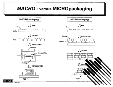
Hybrid Micropackaging of Microdevices
A new approach to vacuum packaging of various microdevices, including
bolometric FPAs,
is being presented. This new, very small-size package structure consists of a
central piece
of machined ceramic or metal to which a small size window made of glass; ZnSe,
Si or (3e
and a microdevice in a die form are being attached using, for example, a
soldering
technique. The central part is equipped with a microchamber and a pump-out
opening.
When the process of attaching the die and the window is completed, the air is
pumped out
from the microchamber via the opening and the opening is subsequently plugged.
Physical vapor deposition of the plugging material is suggested. Each die can
be
packaged separately and each package can be equipped with a dedicated
application
oriented window. Machinable ceramic materfals, such as Macor, are suggested
for the
package central part. The die is attached to the central part via a miniature
spacer
structure which can be produced by machining, electroplating or thin film
deposition. This
spacer is covered with the solder material.
In a different embodiment, the central package parts are machined in a ceramic
wafer.
Then several possibly different windows are attached to the wafer.
Subsequently, the
individual dies are attached to this wafer vis-~-vis the windows and the
wafer, serving as a
tray for the windows and the dies, is sawed into individual packaged devices.
Again, in a different embodiment, the central package parts are machined in a
ceramic
wafer and then the windows are attached to the ceramic wafer. The ceramic
wafer is then
attached to a semiconductor wafer in which the individual microdevices or dies
have been
previously produced. The semiconductor wafer is not sawed but it is in one
piece. After
attaching of the ceramic wafer to the semiconductor wafer, the vacuum pumping
and the
sealing operation is being performed on all devices. Then, the semiconductor
and the
ceramic wafers are sawed into separate individually vacuum packaged devices.
In each of the described embodiments, the semiconductor die is equipped with
standard
bonding pads or through-holes connected to bonding pads placed on the opposite
surface
of the die. In the first case, after completion of the packaging process, the
packaged
devices are connected to external electronics, typically using a standard wire
bonding
technique. In the case of the through-hole, the packaged device can be
directly soldered
to external electronics. Instead of producing the conducting through-holes in
the
semiconductor die, they can be produced in the ceramic central piece of the
package.
These metallzed through-holes have to be connected by soldering or other
methods to the
bonding pads of the semiconductor die.
In each of the described embodiments, if a thermo-electric cooler is being
used, it is placed
outside the package attached directly to the packaged microdevice.
The hybrid micropackaging method and stnrctures are presented in the enclosed
Figures.

Representative Drawing
A single figure which represents the drawing illustrating the invention.
Administrative Status

For a clearer understanding of the status of the application/patent presented on this page, the site Disclaimer , as well as the definitions for Patent , Administrative Status , Maintenance Fee  and Payment History  should be consulted.

Administrative Status

Title Date
Forecasted Issue Date Unavailable
(22) Filed 2000-06-28
(41) Open to Public Inspection 2001-12-28
Dead Application 2002-10-03

Abandonment History

Abandonment Date Reason Reinstatement Date
2001-10-03 FAILURE TO RESPOND TO OFFICE LETTER
2002-01-30 FAILURE TO COMPLETE
2002-06-28 FAILURE TO PAY APPLICATION MAINTENANCE FEE

Payment History

Fee Type Anniversary Year Due Date Amount Paid Paid Date
Application Fee $300.00 2000-06-28
Owners on Record

Note: Records showing the ownership history in alphabetical order.

Current Owners on Record
JEROMINEK, HUBERT
Past Owners on Record
None
Past Owners that do not appear in the "Owners on Record" listing will appear in other documentation within the application.
Documents

To view selected files, please enter reCAPTCHA code :


To view images, click a link in the Document Description column. To download the documents, select one or more checkboxes in the first column and then click the "Download Selected in PDF format (Zip Archive)" or the "Download Selected as Single PDF" button.

List of published and non-published patent-specific documents on the CPD .

If you have any difficulty accessing content, you can call the Client Service Centre at 1-866-997-1936 or send them an e-mail at CIPO Client Service Centre.


Document
Description 
Date
(yyyy-mm-dd) 
Number of pages   Size of Image (KB) 
Representative Drawing 2001-12-04 1 11
Cover Page 2001-12-07 1 27
Description 2000-06-28 1 75
Drawings 2000-06-28 12 373
Correspondence 2000-08-04 1 2
Assignment 2000-06-28 3 80
Correspondence 2001-10-23 1 18