Note: Descriptions are shown in the official language in which they were submitted.
CA 02312834 2000-06-O1
WO 00/14869 PCT/US99/20385
1
CARRIER REUTIL1ZATION FOR SYNCI3RONOUS DETECTION
Technical Field
This Invention relates generally to feed forward systems and, in particular,
to feed
forward systems which control the phase and/or amplitude of the output signal.
Background Art
Io Feed forward correction, invented by Harold S. Black in 1924, is limited in
performance primarily due to variations in system components over power,
temperature, and
time. Several circuits have been employed in order to limit these variations.
These circuits,
however, introduce other limitations.
U.S. Pat. No. 5,051,704 issued to Chapman et al., which is incorporated herein
by
reference, discloses a feed forward amplifier which utilizes a least-means
squared circuit in
order to detect and cancel system errors. The least-means squared circuit,
however, generates
internal errors due to leakage signals inherent in the correlators of the
least-means squared
circuit. These correlators use mixing devices in order to generate an error
signal necessary
for correction. A typical mixer or Gilbert cell typically passes RF signals
from the local
oscillator (LO) and RF port to the intermediate frequency (IF) port whose
output signal is
generally attenuated with respect to the RF port input and varies over time,
temperature and
power. Variations of the IF output over time, temperature, and power limit the
least-means
squared circuit's accuracy to detect and cancel system errors. As a result,
variations over
time, temperature, and power are not entirely eliminated by the above system.
U.S. Pat. No. 5,528,196 issued to Baskin et al., which is incorporated herein
by
reference, discloses a feed forward amplifier in which a differential
phase/amplitude detector
is utilized to control the cancellation of the information signals (i.e., the
carrier signals) at the
output of the summer of the first loop, and an out-of band pilot (reference)
signal is
employed in order to control the distortion signals output by the second loop
so as to cancel
3o distortion signals at the RF output port. The differential phase/amplitude
detector of the first
loop requires separate detectors for each of two RF signals that it receives.
i.e. the RF signal
SUBSTITUTE SHEET (RULE 26)
CA 02312834 2000-06-O1
WO 00/14869 PCT/US99/20385
from the amplifier of the first loop and the KF signal from the RF input port.
Any difference
in efDciency of these detectors over various conditions results in reduced
cancellation of the
information signal by the first loop. Furthermore, even when the differential
phase/amplitude
detector allows cancellation of the information signal at the output of the
summer of the first
loop, the information signals may leak into and infiltrate the low power
stages of the second
loop. The pilot signal for the second loop must be located far out of the
frequency band of
interest, i.e., the frequency band that contains the information signals and
their accompanying
distortion products, in order to avoid errors caused by interference from the
information
signals and accompanying distortion products, and to avoid feedthrough of the
distortion
to products to the output. Accuracy of the control system is limited because
RF performance of
components varies over frequency, thus accuracy out of band does not
necessarily imply in-
band accuracy of the loop. As the pilot signal is outside the frequency band
of interest, it
does not necessarily correct for time, temperature, and power variations
within the frequency
band of interest. Furthermore, as in the first loop, the control system (i.e.,
the loop 2
15 amplitude and phase controller) of the second loop utilizes separate
detectors for each of its
input paths. Any difference in the e~ciency ofthese detectors over various
conditions results
in reduced cancellation of the distortion signals by the second loop.
As a result, there is a need in the art for an RF amplifier feed forward
correction
system that provides stable amplification of the input RF signal over
variations in power,
2o temperature, and time; while avoiding the aforementioned limitations, as
well as others, of
prior art systems.
Disclosure of Invention
In the present invention, only a single detector, rather than multiple
detectors, is used
25 in order to adjust the output of each one of the feed forward loops. In
other words, a first
single detector is used to adjust the output of the first feed forward loop
while a second single
detector is used to adjust the output of the second feed forward loop. The use
of a single
detector to adjust the output of a single feed forward loop eliminates the
problems associated
with using multiple detectors to adjust the output of a single feed forward
loop, namely it
3o eliminates the reduced cancellation due to dii~'erences between the
multiple detectors used to
adjust the output of a single feed forward Loop.
SUBSTITUTE SHEET (RULE 26)
CA 02312834 2000-06-O1
WO 00/14869 PCTNS99/20385 ,
Additionally, in the present invention, the amplified output of the summer of
the first
feed forward loop is used to adjust the output of the first feed forward loop
as well as to
cancel distortion signals at the RF output port. Therefore, leakage of the
carrier signals from
the summer of the first feed forward loop to the second feed forward loop are
accounted for
by the first feed forward loop. In other words, the output of the first feed
forward loop is
adjusted to account for leakage of carrier signals into the summer of the
first feed forward
loop or into the second feed forward loop.
Moreover, the feed forward system of the present invention uses a modulation
signal
(i.e., a signal used to modulate the RF input signal) to synchronously detect
and correct errors
to in the first and second feed forward loops. In other words, the modulation
signal is used to
synchronously adjust the outputs of the first and second feed forward loops.
Furthermore, the
feed forward system of the present invention amplitude detects both phase
modulated signals
and amplitude modulated signals and synchronously detects the modulation
signal in the first
and second feed forward loops in order to adjust the outputs of the first and
second feed
forward loops. The synchronous detection, among other things, allows detection
of signals
below noise level.
The present invention encompasses an amplifier system comprising: an input
signal
port for providing an input signal; a modulating signal source for providing a
modulating
signal; a first feed forward loop coupled to the input signal port and the
modulating signal
2o source, the first feed forward loop modulating the input signal with the
modulating signal,
amplifying a first modulated input signal, outputting a first amplified
modulated signal
including distortion signals, and outputting a first difference signal; a
first synchronous
detection circuit coupled to the first feed forward loop and the modulating
signal source, the
fast synchronous detection circuit outputting a first control signal in
response to the first
difference signal and the modulating signal, wherein the first control signal
controls
modulation of the input signal by the modulating signal such that the first
difference signal
consists of only distortion signals; a second feed forward loop coupled to the
first feed
forward loop, the second feed forward loop modulating the first difference
signal, amplifying
a second modulated input signal, and outputting a second amplified modulated
signal; a
3o second synchronous detection circuit coupled to the second feed forward
loop and the
modulating signal source, the second synchronous detection circuit outputting
a second
SUBSTITUTE SHEET (RULE 26)
CA 02312834 2000-06-O1
WO 00/14869 PCTNS99/20385
control signal in response to a second difference signal which represents a
difference
between the first amplified modulated signal and the second amplified
modulated signal,
wherein the second control signal controls modulation of the first difference
signal in order to
cancel the distortion signals in the first amplified modulated signal by the
second amplified
modulated signal; and an output signal port coupled to the first feed forward
loop and the
second feed forward loop, the output signal port outputting an output signal
that is a function
of the first amplified modulated signal and the second amplified modulated
signal.
The input port receives a radio frequency (RF) input signal. The RF signal is
split, via a coupler, between two paths. The signal of the first path is power
detected by way
of a diode detector; amplitude and/or phase modulated by a signal source
comprising one or
more frequencies (in the preferred embodiment, one frequency is used for
amplitude
modulation, the other frequency is used for phase modulation), via a first
phase and/or
amplitude modulator; then amplified by a first amplifier chain which typically
comprises low
power gain stages and a power amplifier.
In one embodiment, the signal source provides signals at 72.5 kHz and 75.5 kHz
for
phase modulation of the carrier signal and at 73.5 kHz and 74.5 kHz for
amplitude
modulation of the Garner signal. In the preferred embodiment, the signal
source provides
signals which vary in widely in frequency over time about the above mentioned
frequencies.
A means of phase modulation of the input signal can be accomplished in the
following
Zo manner: 1) The signal to be modulated is split using a 3 dB 90°
hybrid coupler. 2) A varactor
diode, used as a voltage variable capacitor, terminates each output port of
the coupler and
reflects substantially all of the signal back into the coupler at an angle
dependant upon a
steering voltage fed to the diodes. The phase modulated output signal is
received from the
isolation port ofthe coupler. Amplitude modulation can be accomplished
similarly in that a
z5 hybrid coupler is utilized as with the phase modulator. A pin diode, used
as a variable
resistor, is utilized in lieu of the varactor diode in order to reflect,
dependant upon a steering
voltage fed to the diodes, a portion of the signal. In other words, if the
resistance of the pin
diodes is equal to the impedance of the coupler (50 ohm), all of the power is
absorbed by the
diodes. If the resistance is lowered, some of the power is reflected out to
the isolation port.
3o The steering voltage is such that a maximum impedance of 50 ohms is
attainable. The
modulation in the first path comprises both trimming and low frequency
modulation of
SUBSTITUTE SHEET (RULE 26)
CA 02312834 2000-06-O1
WO 00/14869 PCT/US99/20385
amplitude and phase.
In one embodiment, a linearization circuit is employed in the first path to
cancel a
substantial amount of the nonlinear signals introduced by the amplifiers.
Linearization can be
accomplished by way of a nonlinear circuit of which the nonlinear portion of
the voltage
output, with respect to the voltage input is opposite that of the amplifier to
be corrected.
The signal of the second path is typically delayed via a delay line to the
same extent
of which the first path causes delay of the input signal.
A sample of the signal output of the first path is combined out of phase with
a sample
of the signal output of the second path, leaving only distortion products at
the output of the
to combining means. Combination can be accomplished with an active device, a
Wilkinson
combiner, or by way of a hybrid coupler, provided that the delay line is
trimmed for proper
cancellation of signals. The above combination is hereon referred to as the
first loop.
A third path receives the distortion products from the combining means,
adjusts the
amplitude and phase, via a second phase and amplitude modulator, then
amplifies the
15 products to a level of which will cancel distortion products at the output
of the system. A
fourth path delays the output of the first path via a delay line to the same
extent of which the
amplifier chain in the third path causes delay of the input signal. The output
of the third path,
which includes primarily distortion products, is then combined, by way of a
coupler, with the
output of the fourth path which includes both distortion products and an
amplified sample of
2o the input signal. The result of the combination is an amplified, low
distortion sample of the
input signal and is the output of the system. The above combination is hereon
referred to as
the second loop.
The modulation of the input signal produces modulation frequency sidebands
used to
detect system alignment. In order to align the first loop, a first amplitude
modulation detector
25 receives a power leveled (AGC) signal from a point along the third path in
order to detect
amplitude and phase alignment errors in the first loop. In the preferred
embodiment, the
output signal from the power detection diode in the first loop is used to
steer attenuators
employed to level the signals received by the amplitude modulation {AM)
detector.
If the first loop is aligned correctly, there is no carrier present in the
third path and,
3o therefore, no modulation frequency detected by the AM detector. If,
however, the output
signal of the first path is high in amplitude, the carrier (input signal) to
modulation sideband
SUBSTITUTE SHEET (RULE 26)
CA 02312834 2000-06-O1
WO 00/14869 PCT/US99/20385
signal is in phase with the carrier to modulation sideband signal of the first
path so that, by
way of carrier to sideband multiplication, a modulation frequency signal,
which is in phase
with the modulation signal at the output of the signal source, is detected by
way of the diode
AM detector. Conversely, if the output signal of the first path is low in
amplitude, the carrier
(input signal) to modulation sideband signal is 180° out of phase with
the carrier to
modulation sideband signal of the first path so that a modulation frequency
signal which is
180° out of phase with the modulation signal is detected. In other
words, the phase of the
frequency between the sidebands and the carrier at the point of combination
with respect to
the corresponding phase of the frequency at the point of modulation determines
the phase of
l0 the detected frequency with respect to that of the signal source.
Similarly, if the output signal of the first path is lagging in phase, the
carrier (input
signal) to modulation sideband signal is in phase with the carrier of the
first path so that a
modulation frequency signal which is in phase with respect to the modulation
signal is
detected. In other words, if the phase of the first path is lagging in phase,
a positive voltage to
the phase modulator causes more lag in phase, lowering the cancellation at the
point of
combination, while a negative going modulation voltage brings the cancellation
at the point
of combination towards alignment, causing an amplitude modulation at the point
of
combination which can be detected with diode or similar AM detector.
Conversely, if the
first path is leading in phase, the Garner (input signal) to modulation
sideband signal is 180°
out of phase with the Garner of the first path so that a modulation frequency
signal which is
180° out of phase with respect to the modulation signal is detected.
A first multiplier receives a bandpass filtered sample from the first
amplitude
modulation detector and a signal from the signal source used for amplitude
modulation and
outputs a corresponding amplitude steering voltage to the first modulator via
a ftrst low pass
filter. In the preferred embodiment, the bandpass filter is configured to pass
frequencies
within the modulation bandwidth and a Gilbert cell is utilized for
multiplication of signals. a
diode mixer may also be utilized. The low pass filter is configured to filter
out any noise
induced by the downconversion process. Similarly, a second multiplier receives
a bandpass
filtered sample from the amplitude modulation detector and a signal from the
signal source
3o used for phase modulation and outputs a corresponding phase steering
voltage to the first
modulator via a second low pass filter.
SUBSTITUTE SHEET (RULE 26)
CA 02312834 2000-06-O1
WO 00/14869 PCT/ElS99/20385
In one embodiment, the multipliers receive the source signals via low pass
filters
configured to delay the source signals equal to the delay at the point of
detection. Another
embodiment utilizes the already present delay line of the second path by way
of a frequency
muitiplexer configured to separate the signal source frequencies from the RF
input
frequencies. The multiplexer comprises a low pass filters) to feed the source
signals} to the
delay line, and from the delay line to the multiplier(s). Series capacitors at
the input and
output of the delay line prevent the source signals) from entering the RF
portion of the
circuitry. In yet another embodiment, the multipliers) receive signals
directly from the signal
source.
A second amplitude modulation detector receives an AGC signal from the output
of
the system in order to detect amplitude and phase alignment errors in the
second loop. Unlike
the detection in the third path, the second amplitude modulation detector
receives a
substantially constant carrier, along with modulation sidebands of which vary
in power and
phase similar to resulting distortion products. If the second loop is
perfectly aligned, the
distortion products, along with the modulation sidebands are cancelled at the
output and there
is no detected signal. If, however, the output signal of the third path is
high in amplitude, the
modulation sideband to carrier (input signal) is 180° out of phase with
the modulation
sideband to carrier signal of the first path so that a modulation frequency
signal which is
180° out of phase with the modulation signal is detected by way of
carrier to sideband
2o multiplication. Conversely, if the output signal of the third path is low
in amplitude, the
modulation sideband to carrier (input signal) is in phase with the modulation
sideband to
carrier signal of the first path so that a modulation frequency signal which
is in phase with
the modulation signal is detected. In other words, the phase of the frequency
between the
sidebands and the carrier at the point of combination with respect to the
corresponding phase
of the frequency at the point of modulation determines the phase of the
detected frequency
with respect to that of the signal source.
Similarly, if the output signal of the third path is lagging in phase, the
carrier (input
signal) to modulation sideband signal is 90° leading in phase with the
carrier of the first path
so that a modulation frequency signal which is 90° leading in phase
with respect to the
3o modulation signal is detected. In other words, if the modulation sideband
signal of the phase
modulated signal is rotated in phase, a phase modulated signal becomes an
amplitude
SUBSTITUTE SHEET (RULE 26)
CA 02312834 2000-06-O1
WO 00/14869 PCT/US99/20385 .-
modulated signal which can be detected with diode or similar detector.
Conversely, if the
first path is leading in phase, the carrier (input signal) to modulation
sideband signal is 90°
lagging in phase with the carrier of the first path so that a modulation
frequency signal which
is 90° lagging in phase with respect to the modulation signal is
detected.
A third multiplier receives a bandpass filtered sample from the second
amplitude
modulation detector and a signal from the signal source used for amplitude
modulation and
outputs a corresponding amplitude steering voltage to the second modulator via
a third low
pass filter. Similarly, a fourth multiplier receives a bandpass filtered
sample from the
amplitude modulation detector and a signal from the signal source used for
phase modulation
to and outputs a corresponding phase steering voltage to the second modulator
via a fourth low
pass filter. The above mentioned multipliers and filters are configured as
those in the first
loop correction circuitry
In one embodiment, the multipliers receive the source signals via low pass
filters
configured to delay the source signals equal to the delay at the point of
detection. Another
15 embodiment utilizes the already present delay lines ofthe second and fourth
path by way of a
frequency multiplexer configured to separate the signal source frequencies
from the input
frequencies. The multiplexer comprises a low pass filters) to feed the source
signals) to the
delay line, and from the delay line to the multiplier(s). Series capacitors at
the input of and
output of the delay lines prevent the source signals) from entering the RF
portion of the
20 circuitry. In yet another embodiment, the multipiier(s) receive signals
directly from the signal
source.
Brief Description of Drawings
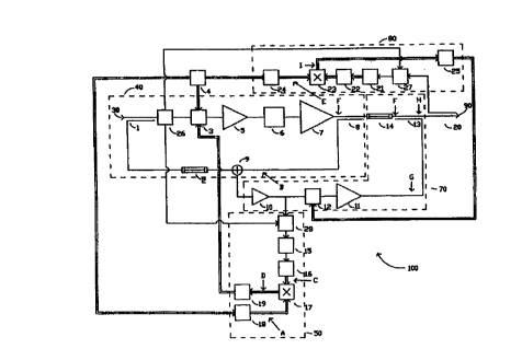
25 Figure I is schematic diagram of a present embodiment of the invention.
Figure 2 shows the signal output by the dual wideband noise source and signals
at
various points within the first synchronous detection circuit under various
phase/amplitude
modulation conditions.
Figure 3 shows the signal output by the dual wideband noise source and signals
at
3o various points within the amplifier system under various amplitude
modulation conditions by
the second feed forward loop.
SU8STtTUTE SHEET (RULE 26)
CA 02312834 2000-06-O1
WO 00/14869 PCTNS99/20385
Figure 4 shows the relation between phase and amplitude modulation.
Best Mode for Carrying Out the Invention
Figure 1 is schematic diagram of a present embodiment of the invention. In
Figure l,
amplifier system 100 comprises an RF input port 30, a first feed forward loop
40, a first
synchronous detection circuit 50, a dual wideband noise source 4, a second
feed forward loop
70, a second synchronous detection circuit 80, and an RF output port 90. Each
of the
synchronous detection circuits may also be herein referred to as a receiver
circuit, a feedback
loop circuit, or a heterodyne synchronous detection circuit.
The RF input port 30 and RF output port 90 are for inputting an RF input
signal into
and outputting an RF output signal from the amplifier system 100,
respectively.
The first feed forward loop 40 includes a coupler 1, a modulator 3, an
amplifier 5
(which may also herein be referred to as a driver amplifier 5), a linearizer
6, an amplifier 7, a
coupler 8, a delay line 2, and a summer 9. The modulator 3 may be a phase
and/or an
amplitude modulator. The first feed forward loop 40 may, as in the present
embodiment of
the invention, also include an amplitude detector, such as amplitude detector
26. Amplitude
detector 26 detects the RF input signal and adjusts the output of the
automatic gain control
(AGC) circuits 27 and 28 so as to maintain the input power to amplitude
detectors 15 and 21
within a reasonable narrow power range even when the RF input power level is
varied.
The first feed forward loop 40 receives an RF input signal (which is also
herein
referred to as the carrier signal) from RF input port 30 and phase and/or
amplitude
modulation signals from the dual wideband noise source 4. The first feed
forward loop
amplitude and/or phase modulates the RF input signal with the modulation
signal(s),
amplifies the modulated RF signal, and outputs an amplified modulated RF
signal, including
distortion signals, to delay line 14 via coupler 8 and distortion signals to
amplifier 10 via
summer 9. The distortion signals may include distortions due to the modulation
and
amplification of the RF input signal, as well as intermodulation signals and
other distortion
signals.
3o Coupler 1 splits the RF input from the RF input port 30 and provides inputs
to the
amplitude detector 26 and the delay line 2. The output of amplitude detector
26 is input to the
SUBSTITUTE SHEET (RULE 26)
CA 02312834 2000-06-O1
WO 00/14869 PCT/US99/20385
modulator 3. The modulator 3 is AC coupled to the dual wideband noise source 4
and
receives modulation signals therefrom. Dual wideband noise source 4 is in a
present
embodiment a frequency sweeper and outputs low frequency signals to the
modulator 3. In
one embodiment, dual wideband noise source 4 provides signals centered at 72.5
and 75.5
5 kHz for phase modulation of the carrier signal by modulator 3 and signals
centered at 73.5
and 74.5 kHz for amplitude modulation of the carrier signal by modulator 3. It
is to be noted
that the dual wideband noise source 4 may be replaced by any signal source or
frequency
generator that generates a modulation signal to be input to modulator 3. For
example, the
dual wideband noise source 4 may be replaced by a dual narrow band noise
source. The
l0 modulation signal acts as a reference or pilot signal, i.e., a known and
identifiable signal
within the system. The signals from the dual wideband noise source 4 are used
by modulator
3 to modulate the signal it receives from amplitude detector 26. The modulator
3 amplitude
and/or phase modulates the signal. Amplitude and phase modulation of a signal
is herein
used to encompass adjustments in the amplitude and phase, respectively, of
that signal, i.e., it
includes DC offset adjustments. The modulated signal is fed from the modulator
3 to the first
amplifier chain, which includes amplifier 5, linearizer 6, and amplifier 7.
The first amplifier
chain amplifies the modulated RF signal and outputs an amplified modulated RF
signal.
Linearizer 6 introduces linearization signals to cancel non-linear signals
introduced by
amplifier 5 and amplifier 7.
2o As stated above, amplifier 7 outputs an amplified modulated RF signal. The
amplified
modulated RF signal includes distortion signals. The distortion signals may
include
distortions due to the modulation and amplification of the RF input signal, as
well as
intermodulation signals and other distortion signals. In the frequency domain,
the amplified
modulated RF signal may be represented by the RF input signal frequency
spectrum (i.e., the
carrier spectrum) and the sideband spectrums, which are due to the modulation
of the RF
input signal. (The sideband spectrums maintain their relative position with
respect to the
carrier spectrum as the carrier is shifted in the frequency domain, i.e., the
pilot signal
spectrum shifts with, or follows, the carrier spectrum as the carrier spectrum
is shifted in the
frequency domain. As a result, the pilot in the present invention remains with
the frequency
3o band of interest and not outside of it.) The output of amplifier 7 is input
to coupler 8. Coupler
8 outputs an attenuated signal to the summer 9 and a substantially
unattenuated signal to
SUBSTITUTE SHEET (RULE 26)
CA 02312834 2000-06-O1
WO 00/14869 PCT/US99/20385
I1
delay line 14. The attenuation at coupler 8 is intended to offset attenuation
of the signal
coupled to delay line 2 by coupler l and the amplification of the modulated
signal by the first
amplifier chain. Delay line 2 is intended to account for the delay in the
signal path from
coupler 1 to the summer 9 via coupler 8. Delay line 2 is also intended to
introduce a 180
degee phase difference, over the desired frequency range, between the signal
that it inputs to
summer 9 and the signal that is input to summer 9 by coupler 8. The output of
delay line 2 to
the summer 9 is an unmodulated and an unamplified version of the original RF
input signal
that is 180 degrees out of phase with respect to the output of coupler 8 to
summer 9. As a
result, the output of summer 9 is intended to consist of only the distortion
signals due to the
io modulation and the amplification of the RF input signal by modulator 3 and
the first
amplif er chain. In other words, the output of the delay line 2 is combined
with equal power,
but a relative I80° phase difference, with the sampled output of
coupler 8 to produce a
difference signal at the output of summer 9 which is intended to consist of
only the distortion
signals.
15 The difference signal is used by both the first synchronous detection
circuit 50 and
the second feed forward loop 70. The difference signal is amplified by
amplifier 10, then fed
into the first synchronous detection circuit 50. The first synchronous
detection circuit 50
includes an automatic gain control (AGC) circuit 28, an amplitude detector 15,
a filter 16, a
dual multiplier chain 17, a low pass filter (LPF) I8 and a dual LPF 19.
20 Filter 16 may be a single or dual LPF. Alternatively filter 16 may be a
single or dual
band pass filter (BPF). In the embodiment shown in Figure 1, filter 16 is a
single BPF. One
BPF in the dual BPF may be used to filter signals that are in a first
frequency band due to
amplitude modulation while the other BPF in the dual BPF may be used to filter
signals that
are in a second frequency band due to phase modulation, where the first
frequency band is
25 different from the second frequency band.
AGC circuit 28, which is controlled by amplitude detector 26, receives the
output of
amplifier 10. It is to be noted that although AGC circuit 28 receives its
input signal from
amplifier 10, AGC 28 may receive its input signal anywhere along the error
amplifier chain,
which includes amplifiers 10 and 11. However, it is more advantageous that AGC
circuit 28
3o receive its input.signal from the error amplifier chain at a point before
the modulator I2. The
AGC circuit 28 feeds its output to the amplitude detector 15. The output of
the AGC circuit
SUBSTITUTE SHEET (RULE 26)
CA 02312834 2000-06-O1
WO 00/14869 PCT/US99120385
I2
28 is adjusted by amplitude detector 26, which detects the RF input signal, so
as to maintain
the input power to amplitude detector 1 S within a reasonably narrow power
range even when
the RF input signal power level is varied. It is to be noted that the AGC
circuit 28 may
receive its adjustment signal from anywhere along the main signal path, which
is the signal
path from the RF input port 30 to RF output port 90 via amplitude detector 26,
modulator 3,
amplifier 5, linearizer 6, amplifier 7, and delay line 14.
The amplitude detector 15 amplitude detects its input and outputs an amplitude
detected signal. In other words, amplitude detector 15 down-converts its input
signal from
the frequency range of the RF input signal to the frequency range of the
signal from the dual
to wideband noise source 4. When the output of summer 9 contains signals other
than the
distortion signals due to phase or amplitude imbalance in the first feed
forward loop 40, then
amplitude detection by amplitude detector 15 provides a wideband noise source
signal that
has the same frequency as the wideband noise source signal output by wideband
noise source
4 and is either substantially in phase or substantially 180 degrees out of
phase with the
respective wideband noise source signal output by the wideband noise source 4.
In other
words, if the first feed forward loop 40 is unbalanced with regard to
amplitude, the signal
provided by amplitude detector 15 is either substantially in phase or
substantially 180
degrees out of phase with the amplitude modulating wideband noise source
signal output by
the dual wideband noise source 4. Similarly, if the first feed forward loop is
unbalanced with
2o regard to phase, the signal provided by amplitude detector 15 is either
substantially in phase
or substantially 180 degrees out of phase with the phase modulating wideband
noise source
signal output by the dual wideband noise source 4. When the output of summer 9
consists of
only distortion signals, then amplitude detection by amplitude detector 15
provides a
wideband noise source signal whose frequency is twice that ofthe respective
wideband noise
source signal output by the dual wideband noise source 4. Amplitude detector
15 may in the
present embodiment be a diode amplitude detector circuit. The amplitude
detected output of
amplitude detector 15 is fed through filter 16 into the dual multiplier chain
17.
The output of the dual wideband noise source 4 is fed into a second set of
ports of the
dual multiplier chain 17 through the single or dual LPF 18. The dual LPF 18
delays the
3o signals from the dual wideband noise source 4 before feeding them into the
dual multiplier
chain 17. Alternatively, delay line 2, or some other delay line, may be used
to delay the
SUBSTITUTE SHEET (RULE 26)
CA 02312834 2000-06-O1
WO 00/14869 PCT/US99/20385
13
signals from the dual wideband noise source 4 prior to feeding the signals to
the dual
multiplier chain 17. V1/hen delay line 2 is used to delay the signals from the
dual wideband
noise source 4, a set of frequency splatters would be used with delay line 2.
The frequency
splatters (which may be a diplexor) include a first low capacitance capacitor
(not shown)
coupled between coupler 1 and delay line 2, a second low capacitance capacitor
(not shown)
coupled between delay line 2 and summer 9, a first inductor (not shown)
coupled between the
dual wideband noise source 4 and the delay line 2, and a second inductor (not
shown)
coupled between the delay line 2 and the dual multiplier chain 17, where each
of the first and
second inductors has an inductance that is high enough to block transmission
of the RF input
l0 signal yet low enough to allow transmission of the signals from the dual
wideband noise
source 4.
One multiplier in the dual multiplier chain 17 is used to multiply signals
from one
wideband noise source in the dual wideband noise source 4 while the other
multiplier in the
dual multiplier chain 17 is used to multiply signals from the other wideband
noise source in
the dual wideband noise source 4. A dual wideband noise source is used to
allow phase and
amplitude modulation to be done using modulating signals having different
frequencies.
By multiplying the signal received from amplitude detector 15 via filter 16
with the
signal received from the dual wideband noise signal source 4 via dual LPF 19,
the dual
multiplier chain 17 converts the signals detected by the amplitude detector 15
to the
respective frequency of the signal from the dual wideband noise source 4, but
with an
included DC offset which is due to the phase and/or amplitude modulation error
of the RF
input signal by the modulator 3. The output of the dual multiplier chain 17 is
then fed,
through the dual LPF 19, to the modulator 3.
The signal fed through dual LPF 19 to the modulator 3 controls the attenuation
of the
RF input signal by the modulator 3 such that there is maximum cancellation of
the RF input
signal at the output of summer 9. Thus, the signals from the dual wideband
noise source 4 are
used to modulate the RF input signal by modulator 3 as well as to control the
attenuation/phase of the RF input signal by modulator 3 so as to provide
maximum
cancellation of the RF input signal at the output of summer 9.
3o A positive DC output from dual LPF 19 causes modulator 3 to increase the
attenuation of the RF input signal so as to reduce the amplitude of the output
of amplifier 7
SUBSTITUTE SHEET (RULE 26)
CA 02312834 2000-06-O1
WO 00!14869 PCT/US99/20385
14
such that the output of summer 9 consists of only distortion signals. A
negative DC output
from dual LPF 19 causes modulator 3 to reduce the attenuation of the RF input
signal so as to
increase the amplitude of the output of amplifier 7 such that the output of
summer 9 consists
of only distortion signals.
For phase modulation, adjustments analogous to those in the previous paragraph
are
made in response to outputs from the dual LPF 19 to modulator 3. A positive DC
output from
dual LPF 19 causes modulator 3 to increase the phase of the RF input signal so
as to reduce
the phase of the output of amplifier 7 such that the output of summer 9
consists of only
distortion signals. A negative DC output from dual LPF 19 causes modulator 3
to reduce the
1o phase of the RF input signal so as to increase the phase of the output of
amplifier 7 such that
the output of summer 9 consists of only distortion signals.
Figure 2 shows the signal output by the dual wideband noise source 4 and
signals at
various points within the first synchronous detection circuit 50 under various
phase and/or
amplitude error conditions.
When the phase/amplitude of the output of amplifier 7 is ideal,
phase/amplitude error
signal (B), which is the signal at point (B), in Figure 1, referenced to the
phase and amplitude
of the signal output by delay line 2, is perfectly symmetrical about the zero
error axis 200
(i.e., the lobes above the zero error axis 200 are equal to the lobes below
the zero error axis
200). In other words, when the phase/amplitude of the output of amplifier 7 is
ideal, the
2o output of summer 9 consists of only distortion signals. Also, when the
phase/amplitude of the
output of amplifier 7 is ideal, the output of amplitude detector 15,
represented by the signal at
point (C), in Figure 1, has a frequency that is exactly twice the frequency of
the modulation
signal output by the dual wideband noise
source 4. Thus, when the phase/amplitude of the output of amplifier 7 is
ideal, the phase and
amplitude modulation vary the cancellation at the output of the summer 9 to
provide an
output signal from summer 9 that has double frequency of the signal output by
the dual
wideband noise source. In other words, the first feed forward loop 40 in
conjunction with the
first synchronous detection circuit 50 acts as a frequency doubler. Finally,
when the
phase/amplitude ofthe output of amplifier 7 is ideal, the output of dual
multiplier chain
3o provides no DC adjustment. As a result the attenuation/phase adjustment of
the RF input
signal at the modulator 3 is unaffected.
SUBSTITUTE SHEET (RULE 26)
CA 02312834 2000-06-O1
WO 00/14869 PCTlUS99/20385
When the phase/amplitude of the output of amplifier 7 is high, the
phase/amplitude
error (B) is shifted upward with respect to the zero error axis 200.
Furthermore, the
amplitude detection signal (C) has uneven lobes with the larger lobes
corresponding to the
positive half cycles of the noise source output (A). Thus, the multiplier
output (D) has a
5 positive DC offset. The dual LPF 19 sends a positive DC signal to the
modulator 3 which
causes modulator 3 to increase the attenuation/phase adjustment of the RF
input signal prior
to modulation. The increased attenuation/phase adjustment of the RF input
signal causes the
amplitude/phase of the output of amplifier 7 to decrease. This increase in the
attenuation of
the RF input signal in modulator 3 continues until the lobes at (C) are no
longer uneven.
to When the phase/amplitude of the output of amplifier 7 is low, the
phase/amplitude
error (B) is shifted downward with respect to the zero error axis 200.
Furthermore, the
amplitude detection signal (C) has uneven lobes with the larger lobes
corresponding to the
negative half cycles of the noise source output (A). Thus, the multiplier
output (D) has a
negative DC offset. The dual LPF 19 sends a negative DC signal to the
modulator 3 which
15 causes modulator 3 to reduce the attenuation/phase adjustment of the RF
input signal prior to
modulation. The reduced attenuationlphase adjustment of the RF input signal
causes
amplitude/phase of the output of amplifcer 7 to increase. This reduced
attenuation of the RF
input signal in modulator 3 continues until the continues until the lobes at
(C) are no longer
uneven.
2o Referring back to Figure l, as mentioned above, the difference signal is
also input to
the second feed forward loop 70. The second feed forward loop 70 includes an
amplifier 10,
a modulator 12, an amplifier 11, a delay line 14 and a coupler 13. The
amplifier 10 and 11
are part of the error amplifier chain. The difference signal is amplified by
amplifier 10. The
output of the amplifier 10 is fed to modulator 12. Modulator 12, which may be
a phase and/or
amplitude modulator, modulates the input from amplifier 10 and feeds its
modulated output
signal to amplifier 11. It is to be noted that, as in the case of modulator 3,
the amplitude and
phase modulation of a signal by modulator 12 is herein used to encompass
adjustments in the
amplitude and phase, respectively, of that signal, i.e., it includes DC offset
adjustments.
Amplifier 11 amplifies the modulated signal it receives from modulator 10 and
feeds its
3o amplified modulated output to coupler 13. Coupler 13 injects the amplified
modulated signal
it receives from
SUBSTITUTE SHEET (RULE 26)
CA 02312834 2000-06-O1
WO 00/14869 PCT/U599/20385 ..
16
amplifier 11 at point H so as to be combined with the output of delay line 14;
The output of
amplifier 11 represents distortion signals. Delay line 14 delays the output it
receives from
coupler 8 and outputs a delayed signal that is 180 degrees out of phase with
respect to the
signal injected by coupler 13. The signal output by delay line 14 is a delayed
version ofthe
amplified modulated signal output by amplifier 7. As mentioned above the
amplified
modulated signal output by amplifier 7 includes distortion signals due to the
modulation and
amplification in the first feed forward loop 40. Moreover, the distortion
output by delay line
14 is 180 degrees out of phase with respect to the distortion signal output by
amplifier 11.
The RF output port 90 outputs an: output signal that is the sum of the output
of delay line 14
to and the amplifier 11. The attenuation and phase shifting at modulator 12 is
controlled by the
second synchronous detection circuit 80 such that the output of amplifier 11
cancels the
distortions in the amplified modulated RF input signal output by
delay line 14.
The second synchronous detection circuit 80 includes coupler 20, AGC circuit
27,
amplitude detector 21, filter 22, dual multiplier chain 23, LPF 24 and dual
LPF 25. Filter 22
may be a single or dual LPF. Alternatively, filter 22 may be a single or dual
BPF. In the
embodiment shown in Figure I, filter 22 is a single BPF.
As in the first synchronous detection circuit 50, use of dual elements within
the
second synchronous detection circuit 80 allows simultaneous processing of two
signals of
different frequencies. One element in a dual element set processes signals
having a first
frequency while a second element in the dual element set processes signals
having a second
frequency.
The RF output signal of the system, which is the sum of the output of
amplifier 11
and delay line 14, is sampled via output coupler 20 and fed to the AGC circuit
27. The AGC
circuit 27, which is controlled by amplitude detector 26, feeds its output to
the amplitude
detector 21. The output of AGC circuit 27 is adjusted by amplitude detector
26, which
detects the RF input signal, so as to maintain the power input to amplitude
detector 21 within
a reasonably narrow power range when the RF input power is varied.
The amplitude detector 21 amplitude detects its input and outputs an amplitude
detected signal. Amplitude detector 21, like amplitude detector 15, may in the
present
embodiment be a simple diode amplitude detector. The amplitude detected output
of
SUBSTITUTE SHEET (RULE 26)
CA 02312834 2000-06-O1
WO 00/14869 PCT/US99/20385 ~-
17
amplitude detector I S is fed through filter 22 into the dual multiplier chain
23. The output of
the dual wideband noise source 4 is fed into a second set of ports of the dual
multiplier chain
23 through LPF 24.
The LPF 24 delays the signals from the dual wideband noise source 4 before
feeding
it into the dual multiplier chain 23. Alternatively, delay line 2 and delay
line 14, or some
other delay line or lines, may be used to delay the signals from the dual
wideband noise
source 4 prior to feeding the signals to the dual multiplier chain 23. When
delay line 2 and
delay line 14 are used to delay the signals from the dual wideband noise
source 4, a set of
frequency splitters (which may be diplexors) would be used with delay line 2
and delay line
l0 14. The frequency splitters used in conjunction with delay line 2 would
include a first low
capacitance capacitor (not shown) coupled between coupler 1 and delay Line 2,
a second low
capacitance capacitor (not shown) coupled between delay line 2 and summer 9, a
first
inductor (not shown) coupled between the dual wideband noise source 4 and the
delay line 2.
a second inductor (not shown) coupled between the
delay line 2 and the dual multiplier chain 23, where each of the first and
second inductors has
an inductance that is su~ciently high so as to block transmission of the RF
input signal yet is
sufficiently low so as to allow transmission of the signals from the dual
wideband noise
source 4. The frequency splitters used in conjunction with delay line 14 would
include a first
low capacitance capacitor (not shown) coupled between coupler 8 and delay line
14, a second
2o low capacitance capacitor (not shown) coupled between delay line 14 and
point H, a first
inductor (not shown) coupled between the dual wideband noise source 4 and the
delay line
14, a second inductor (not shown) coupled between the delay line 14 and the
dual multiplier
chain 23, where each ofthe first and second inductors has an inductance that
is sufficiently
high so as to block transmission of the RF input signal yet is sufficiently
low so as to allow
transmission of the signals from the dual wideband noise source 4.
One multiplier in the dual multiplier chain 23 is used to multiply signals
from one
wideband noise source in the dual wideband noise source 4 while the other
multiplier in the
dual multiplier chain 23 is used to multiply signals from the other wideband
noise source in
the dual wideband noise source 4. A dual wideband noise source is used to
allow phase and
3o amplitude modulation to be done using modulating signals having different
frequencies.
By multiplying the signal received from amplitude detector 21 via filter 22
with the
SUBSTITUTE SHEET (RULE 26)
CA 02312834 2000-06-O1
WO 00114869 PCTNS99/20385
18
signal received from the dual wideband noise signal source 4 via LPF 24, the
dual multiplier
chain 17 converts the signals detected by the amplitude detector Z1 to double
the frequency
of the signal from the dual wideband noise source 4, but with an included DC
offset which is
due to the phase and/or amplitude modulation of the RF output signal.
The output of the dual multiplier chain 23 is then fed, through the dual LPF
25, to the
modulator 12. The signal fed through dual LPF 25 to the modulator 12 controls
the
attenuation/phase adjustment of the difference signal by the modulator 12 such
that there is
maximum cancellation of the distortion signals at the RF output port 90. Thus,
the signals
from the dual wideband noise source 4 are used to modulate the RF input signal
by
to modulator 3, to control the attenuation of the RF input signal by modulator
3 so as to provide
maximum cancellation of the RF input signal at the output of summer 9, and to
control the
attenuation/phase adjustment of the distortion or difference signal by
modulator 12 so as to
provide maximum cancellation of the distortion signals at the RF output port
90.
Figure 3 shows the signal output by the dual wideband noise source 4 and
signals at
15 various points within the amplifier system 100 under various amplitude
modulation
conditions by the second feed forward loop 70.
Under ideal phase/amplitude modulation conditions in the second feed forward
loop
70, the amplitude modulation (F), i.e., the signal at point (F), in Figure 1,
due to modulation
in the first feed forward loop 40, is of equal amplitude but of opposite phase
(i.e., 180 degrees
20 out of phase) with respect to the output of amplifier 11, i.e., amplitude
correction (G). The
sum of amplitude modulation (F) and amplitude modulation (G) is zero at point
(H) and thus
the residual modulation at point (H) is zero. In other words the distortion
signal from the
second feed forward loop 70 perfectly cancels the distortion signals in the
amplified
modulated signal output by the amplifier 7. Consequently, the multiplier
output (I) is also
25 zero and the modulation of the modulator 12 is not changed.
Under high amplitude modulation conditions in the second feed forward loop 70,
the
amplitude correction (G) is out of phase with and larger in amplitude than the
amplitude
modulation{F}. Therefore, the residual modulation (I-I) is out ofphase with
the amplitude
modulation(F}. The detected modulation at AM detector 21 is also out of phase
with the
3o noise source output (E). Consequently, the multiplier output (I) has a
negative DC offset and
has twice the frequency of the noise source output (E). The negative DC offset
is applied to
SUBSTITUTE SHEET (RULE 26)
CA 02312834 2000-06-O1
WO 00/14869 PCT/US99/20385
19
the modulator 12 via dual LPF 25 and causes the modulator 12 to increase the
attenuation of
the signal which it modulates. This increased attenuation causes the amplitude
correction (G)
to reduce in amplitude. This increased attenuation is continued until the
detection at AM
detector 21 is eliminated.
Under low amplitude modulation conditions in the second feed forward loop 70,
the
amplitude correction (G) is out of phase with and smaller in amplitude than
the amplitude
modulation (F). Therefore, the residual modulation (IT) is in phase with the
amplitude
modulation (F). The detected modulation at AM detector 21 is also in phase
with the noise
source output (E). Consequently, the multiplier output (I) has a positive DC
offset and has
to twice the frequency of the noise source output (E). The positive DC offset
is applied to the
modulator 12 via dual LPF 25 and causes the modulator 12 to reduce the
attenuation of the
signal which it modulates. This reduced attenuation causes the amplitude
correction (G) to
increase in amplitude. This increased attenuation is continued until the
detection at AM
detector 21 is eliminated.
For phase modulation, adjustments analogous to those for amplitude modulation
are
made at modulator 12. Under ideal phase/amplitude modulation conditions, the
phase at
modulator 12 is not changed. Under high phase modulation conditions, a
negative DC offset
is applied to the modulator 12 via dual LPF 25 and causes the modulator 12 to
decrease the
phase of the signal which it modulates. This phase decrease causes the phase
of the
2o modulation at error amplifier output (G) to decrease. The decrease in phase
modulation is
continued until the multiplier output (I) is eliminated, i.e., is zero. Under
low phase
modulation conditions, a positive DC offset is applied to the modulator 12 via
dual LPF 25
and causes the modulator 12 to decrease the phase of the signal which it
modulates. This
phase decrease causes the phase modulation at modulator 12 to increase. The
increase in
phase modulation is continued until the detection at AM detector 21 is
eliminated.
Figure 4 shows the relation between phase and amplitude modulation. In Figure
4, for
phase modulation, vector 401 represents the carrier spectrum while vectors 402
and 403
represent the sideband spectrums. Similarly, for amplitude modulation, vector
451 represents
the carrier spectrum while vectors 452 and 453 represent the sideband
spectrums. Vector 491
represents the carrier spectrum for a reference amplitude modulation signal
while vectors 492
and 493 represent the sideband spectrums for the reference amplitude
modulation signal. The
SUBSTITUTE SHEET (RULE 26)
CA 02312834 2000-06-O1
WO 00/14869 PCTlUS99/2-0~85 ..
length of each vector indicates the amplitude of the spectrum represented by
that vector. The
horizontal distance between the base point of two vectors represents the
frequency spread
between the spectrums represented by the two vectors. The direction in which a
vector points
indicates the relative phase of the signal represented by the vector. For
example, vectors 401
5 and 402 both point upward in the vertical direction. Similarly, vectors 491
and 492 also point
upward in the vertical direction. Therefore, the relative phase of vectors 401
and 402 is in
phase with the relative phase of vectors 491 and 492. Vector 403 points
downward and is,
therefore, out of phase with vector 493, which points downward in the vertical
direction.
Also, the frequency difference between the signals represented by vectors 402
and 401 is
to identical to and out of phase with the frequency difference between the
signals represented
by vectors 403 and 401. As a result, the combination of signals represented by
vectors 401,
402, and 403 is a signal of constant amplitude that is phase modulated. The
signal
represented by vector 452 has a positive 90 degree with respect to the signal
represented by
vector 492. The signal represented by vector 453 has a negative 90 degree
phase with respect
15 to the signal represented by vector 493. Also, the frequency difference
between signals
represented by vectors 452 and 451 is identical to and in phase with the
frequency difference
between the signals represented by vectors 453 and 451. As a result, the
combination of
signals represented by vectors 451, 452, and 453 is a signal having a varying
amplitude and
thus is amplitude modulated. As can be seen in Figure 4, the difference
between the vectors
2o for the amplitude and phase modulation is limited to the difference in the
orientation of the
sideband vector 402 and its corresponding sideband vector 452 and the
difference in the
orientation of the sideband vector 403 and its corresponding sideband vector
453. If vector
402 is rotated counterclockwise (i.e., towards the left) by 90 degrees about
its base point,
then it would have the same orientation as vector 452. This indicates vectors
402 and 452 are
90 degrees out of phase with respect to each other. Similarly, if vector 403
is rotated
clockwise (i.e., towards the right) by 90 degrees about its base point, then
it would have the
same orientation as vector 453. This indicates that vectors 403 and 453 are
also 90 degrees
out of phase with respect to each other. Thus, phase modulation will convert
to amplitude
modulation if the phase of the difference frequency between one side band and
the carrier is
3o delayed by 90 degrees, and if the difference frequency between the
remaining side band and
the carrier is advanced by 90 degrees, or , more generally, if the total
rotation difference
SUBSTITUTE SHEET (RULE 26)
CA 02312834 2000-06-O1
WO 00/14869 PCTNS99/2-0385
21
between the two sideband signals with respect to the carrier signal is equal
to I 80 degrees.
Therefore, introducing a 90 degree phase shift in the sidebands of an
amplitude modulated
signal would generate the sidebands that would have been achieved by phase
modulation of
the original signal. Similarly, introducing a 90 degree phase shift in the
sidebands of a phase
modulated signal would generate the sidebands that would have been achieved by
amplitude
modulation of the original signal. Note that the corresponding modulation is
delayed 90
degrees for phase to amplitude conversion when the sidebands are shifted
positively in phase
and is advanced by 90 degrees for an amplitude to phase conversion when the
sidebands are
shifted positively in phase. The converse is true when the sidebands are
shifted negatively in
to phase.
The above relation between phase and amplitude modulation allows using
amplitude
detectors to detect phase modulation in the following manner. if the output of
amplifier 11
lags in phase, the sidebands of the output of amplifier I 1 combine with the
carrier signal at F,
lagging in phase by 90 degrees with respect to the sidebands at F. This
produces amplitude
modulation which, when amplitude detected, is 90 degrees lagging in phase with
respect to
the phase modulating wideband noise source signal at coupler 20. This
amplitude modulation
is detected by amplitude detector 21 by way ofthe AGC circuit 27. A 90 degree
phase shifted
and delayed signal from the wide band noise source 4 used to phase modulate a
carrier by
modulator 3 is multiplied by a filtered version of the output of amplitude
detector 21 using
2U the phase portion of dual multiplier chain 23, i.e., the multiplier in dual
multiplier chain 23
used for multiplying phase modulation related signals. The output of dual
multiplier chain 23
contains a double frequency of the phase portion of dual multiplier chain 23
and a positive
DC voltage. The DC voltage from the phase portion of dual multiplier chain 23
is filtered by
one LPF in the dual LPF 25 and causes modulator 12 to lead in phase.
Conversely, if the
output of amplifier I 1 leads in phase, the sidebands of the output of
amplifier 11 combine
with the carrier signal at F, leading in phase by 90 degrees with respect to
the sidebands at F.
This produces amplitude modulation, which, when amplitude detected. is 90
degrees leading
in phase with respect to the phase modulating wideband noise source signal at
coupler 20.
This amplitude modulation is detected by amplitude detector 21 by way of AGC
circuit 27. A
90 degree phase shifted and delayed signal from the wide band noise source 4
used to phase
modulate a carrier by modulator 3 is multiplied by a filtered version ofthe
output of
SUBSTITUTE SHEET (RULE 26)
CA 02312834 2000-06-O1
WO 00/14869 PCT/US99/20385
22
amplitude detector 21 using the phase portion of the dual multiplier chain 23.
The output of
dual multiplier chain 23 contains a double frequency of the signal input to
the phase portion
of dual multiplier chain 23 and a negative DC voltage. The DC voltage from the
phase
portion of dual multiplier chain 23 is filtered by one LPF in the dual LPF 25
and causes
modulator 12 to lag in phase.
While the present invention has been particularly described with respect to
the
illustrated embodiments, it will be appreciated that various alterations,
modifications and
adaptations may be made based on the present disclosure, and are intended to
be within the
scope of the present invention. While the invention has been described in
connection with
1o what are presently considered to be the most practical and preferred
embodiments, it is to be
understood that the present invention is not limited to the disclosed
embodiment but, on the
contrary, is intended to cover various modifications and equivalent
arrangements included
within the scope of the appended claims.
Industrial Apnlicabilitv
The disclosed embodiment may be utilized order to provide linearization to any
nonlinear amplifier. The application applies to electromagnetic transmission
amplifiers,
particularly those utilized in the cellular communication field.
SUBSTITUTE SHEET (RULE 26)