Note: Descriptions are shown in the official language in which they were submitted.
CA 02312845 2000-06-O1
WO 99/31698 PCT/US98/26379
TITLE OF INVENTION
SELF-GETTERING ELECTRON FIELD EMITTER AND FABRICATION PROCESS
TECHNICAL FIELD
This invention relates generally to microelectronic devices utilizing field
emission
and fabrication methods for such devices, and more particularly to fabrication
of electron
to field emitter structures having self Bettering properties.
BACKGROUND ART
A difficult challenge in fabricating electron field-emission arrays, such as
those used in
field-emission displays, is providing a Better material effective for
preventing the electron
1s emitters from becoming contaminated. Typically in field-emission displays,
a Better
material is placed at the outer edge of the entire array. Since the width and
length of a
typical display can be several tens of centimeters, and the distance between
the emitter
and anode of each cell is typically on the order of only 50 to 200
micrometers, a Better
material can be disposed too far away from many emitters of the array to
effectively
2o Better decomposition products or outgassed species. The result can be
contamination of
the emitter, causing changes in work function, with resulting catastrophic
failure of the
field-emission array.
NOTATIONS AND NOMENCLATURE
25 In this specification, the term "nitrided" as applied to metals, for
example "nitrided
tantalum" or "nitrided molybdenum" will refer not only to a stoichiometric
nitride
compound such as TaN, Ta,N, MoN, or Mo2N, but also to non-stoichiometric
partially
CA 02312845 2000-06-O1
WO 99/31698 PCT/US98/26379
nitrified metal, i.e. a metal to which an amount of nitrogen has been added,
though not
necessarily an amount necessary to form a stoichiometric compound. Formulas
for su-
materials are often written as MoNx or Ta,~N, for example. It is known in the
art that
various amounts of nitrogen can be introduced into thin films of metals, for
example ~ ,
reactive sputtering or ion implantation, to produce non-stoichiometric
nitrified
compositions.
The term "lateral" in this specification refers generally to a direction
parallel to a
substrate on which an electronic device is formed. Thus a "lateral field-
emission device"
to refers to a field-emission device formed on a substrate and formed with a
structure such
that an anode is spaced apart from a field emitter along at least a direction
parallel to the
substrate. Similarly, the term "lateral emitter" refers to a field emitter
made substantially
parallel to the substrate of a lateral device, whereby emission of electrons
toward the
anode occurs generally parallel to the substrate. Examples of such lateral
emitters
15 formed of thin films are known in the related art.
While some authorities have restricted the term "gettering" to mean clean-up
of residual
gases and gas or other contaminants produced during processing of devices, and
have
used the term "keeping" to mean the clean-up of gas or other contaminants
produced
zo during life of the devices, the term "gettering' in this specification and
the appended
claims is intended to encompass all such applications. The term "contaminants"
is
intended to encompass any unintended or unwanted substance that can affect the
electron emission from an emitter of a electron field emission device. Such
contaminants
may be atoms, molecules, atom clusters, ions, free radicals, etc. Common
potential
25 molecular contaminants include, for example, 02, H2, S02, N2, NH3, C02, CO,
H20,
C2H2, CZH4, CH4, SF6, and CCI2F2.
2
CA 02312845 2000-06-O1
WO 99/31698 PCT/US98/26379
RELATED AR1'
Many field-emission device structures are known, of which it appears a
majority have
been generally of the Spindt type, as described for example in U.S. Pat. No.
3,755,704.
The following U.S. patents describe various field emission devices having
lateral field
emitters and/or their fabrication processes: Cronin et al. 5,233,263 and
5,308,439; Xie et
al. 5,528,099; and Potter 5,616,061, 5,618,216, 5,628,663, 5,630,741,
5,644,188,
5,644,190, 5,647,998, 5,666,019, 5,669,802, 5,700,176, and 5,703,380.
The use of getter pumping to remove gases from an environment has been known
for
many years. More recently, gettering has been used in field-emission devices
with
to various methods and arrangements to prevent the electron-emitting tip from
being
contaminated.
U.S. Pat. No. 4,041,316 to Todokoro et al. discloses a field emission electron
gun with an
evaporation source, the evaporating material from which forms evaporation
layers on the
t5 inner surface of the vacuum chamber and the anode surface. Reactive gases
adhering to
and embedded into the inner surface of the vacuum chamber and the anode are
suppressed from being drawn out by electron bombardment.
U.S. Pat. No. 5,063,323 to Longo et al. discloses a structure providing
passageways for
2o venting of outgassed materials. Outgassed materials, liberated in spaces
between pointed
field emitter tips and an electrode structure during electrical operation of a
field emitter
device, are vented through passageways to a pump of gettering material
provided in a
separate space.
25 U.S. Pat. No. 5,223,766 to Nakayama et al. discloses a thin type of image
display device
for displaying an image by emitting light from a phosphor upon irradiation
with electron
beams. The device has a cathode panel between a front panel and a back panel
in such a
3
CA 02312845 2000-06-O1
WO 99/31698 PCTlUS98/26379
manner that a space exists between the cathode panel and the back panel.
Through-hoses
for diffusion of Betters are formed in the cathode panel to maintain the image
quality at
the center of a display screen, or the cathode panel is supported by Betters
to maintain a
required pressure for attaining a higher image quality even on a Large-sized
display
screen. A gate electrode in this device may be composed of a Better material.
U.S. Pat. Nos. 5,453,659 and 5,520,563 to Wallace et al. disclose an anode
plate for use
in a field emission flat panel display having integrated Better material. The
anode plate
comprises a transparent planar substrate having a plurality of electrically
conductive,
to parallel stripes comprising the anode electrode of the device. The stripes
are covered by
phosphors, and there is a Bettering material in the interstices of the
stripes. The Bettering
material is preferably zirconium-vanadium-iron or barium.
U.S. Pat. No. 5,498,925 to Bell et al. discloses a flat panel display
apparatus which
t5 includes spaced-apart first and second electrodes, with a patterned solid
material layer in
contact with one of the electrodes, exemplarily between the two electrodes.
The
patterned layer (referred to as the "web") includes a multiplicity of
apertures, with at least
one aperture associated with a given pixel. In the aperture is disposed a
quantity of a
second material, exemplarily, a phosphor in the case of an FPFED, or a color
filter
2o material in the case of a LCD. The web can include Better or hygroscopic
material.
U.S. Pat. No. 5,502,348 to Moyer et al. discloses a ballistic charge transport
device with
integral active contaminant absorption means. The ballistic charge transport
device
includes an edge electron emitter defining an elongated central opening
through it, with a
25 receiving terminal (e.g. an anode) at one end of the opening and a Better
at the other end.
A suitable potential is applied between the emitter and the receiving terminal
to amact
emitted electrons to the receiving terminal, and a different suitable
potential is applied
4
CA 02312845 2000-06-O1
WO 99/31698 PCT/US98/26379
between the emitter and the getter so that contaminants, such as ions and
other
undesirable particles, are accelerated toward and absorbed by the getter.
U.S. Pat. No. 5,545,946 to Wiemann et al. discloses a field emission display
which
includes an insulating layer and an emitting layer disposed on the faceplate.
A vacuum
chamber is disposed between a backplane and the emitting layer and contains a
getter.
Apertures are defined through the insulating layer and the emitting layer for
communicating contaminants from the faceplate to the vacuum chamber.
1o U.S. Pat. No. 5,578,900 to Peng et al. discloses a field emission display
having a built-in
ion pump for removal of outgassed material. Ion pump cathode electrodes formed
of a
gettering material cover the gate electrodes, so that during display
operation, the
outgassed material is collected at the ion pump cathode electrodes.
Alternately, the ion
pump cathode may be formed on a focusing electrode, on a focusing mesh, or on
other
electrode structures.
U.S. Pat. No. 5,606,225 to Levine et al. discloses a tetrode arrangement for a
color field-
emission flat panel display with barrier electrodes on the anode plate. The
anode plate
inciudes a transparent planar substrate having on it a layer of a transparent,
electrically
2o conductive material, which comprises the anode electrode of the display
tetrode. Barrier
structures comprising an electrically insulating, preferably opaque material,
are fornled
on the anode electrode as a series of parallel ridges. Atop each barrier
structure are a
series of electrically conductive stripes, which function as deflection
electrodes. The
conductive stripes are formed into three series such that every third stripe
is electrically
interconnected. The deflection electrodes may be formed of a conductive
material having
gettering qualities, such as zirconium-vanadium-iron.
5
CA 02312845 2000-06-O1
WO 99!31698 PCTNS98/26379
U.S. Pat. No. 5,610,478 to Kato et al. discloses a method of conditioning
emitters of a
field emission display to improve electron emission. Emitters and rows are
operated at
voltages that stimulate electron emission from the emitters. An anode is
operated at a
voltage that does not attract electrons so that the electrons are attracted to
the rows.
U.S. Pat. No. 5,614,785 to Wallace et al. discloses an anode plate for flat
panel displays
having a silicon Better. The display device includes a transparent substrate
having a
plurality of spaced-apart, electrically conductive regions forming the anode
electrode,
covered by a luminescent material. A Better material of porous silicon is
deposited on
to the substrate between the conductive regions of the anode plate. The Better
material of
porous silicon is preferably electrically nonconductive, opaque, and highly
porous.
U.S. Pat. No. 5,635,795 to Itoh et al. discloses a Better chamber for flat
panel displays. A
fluorescent display device includes an air-tight envelope having a cathode
substrate, an
15 anode substrate with a phosphor layer arranged to provide a luminous
display, a seal
member, an evacuation hole formed at a side of the envelope, and a Better
chamber in
communication with the hole. The Better chamber is disposed on the outside of
the
envelope and includes a chamber body and an evacuation tube. The Better
chamber
eliminates the independent formation of an evacuation hole in the cathode
substrate and
2o thereby prevents damage and contamination of the cathode substrate.
U.S. Pat. No. 5,656,889 to Niiyama et al. discloses a Better device capable of
being
re-activated as required and arranged in a narrow space in an envelope. The
Better is
arranged in a layer-like manner in an envelope of an electronic element to
provide, in the
z5 envelope, a film-like Better for keeping the interior of the envelope at a
vacuum.
Electrons emitted from an electron feed section are impinged on the Better to
activate it.
6
CA 02312845 2000-06-O1
WO 99/31698 PCT/US98/26379
Thus several field-emission devices of the background art have included
Bettering
material associated with the inner surface of vacuum chamber walls or
associated with the
anode, gate, or deflection electrodes of the devices.
DISCLOSURE OF INVENTION
PROBLEMS SOLVED BY INVENTION
There are many sources of contamination that can affect the performance of
electron field
emitters, including the outgassing of materials used in fabrication of the
devices, electron-
io stimulated decomposition, electron-stimulated desorption, residual gases
present in
vacuum systems used during device fabrication, and permeation of gases into
the ambient
environment of the field emitter. The present invention provides improved
means for
preventing contamination of electron field emitters, thus preventing undesired
changes in
the electron field emitters' work functions, which can otherwise cause
improper
15 functioning of the field-emission devices or arrays of such devices.
OBJECTS AND ADVANTAGES OF INVENTION
A main purpose of the invention is preventing an electron field emitter from
becoming
contaminated and thus preventing undesirable changes in the field emitter's
work
2o function. Thus a general object is a more reliable electron field emitter
device.
Therefore, one object of the invention is Bettering potentially contaminating
atoms,
molecules, and ions from an evacuated space or ambient gas near an electron
field emitter
and especially near the field emitter's emitting tip. A particular object is
providing a self
Bettering electron field emitter. A similar object is providing a Bettering
material integral
25 with an electron field emitter. A related object is a Better that will
automatically have the
same negative potential as the emitter, for improving the attraction and
Bettering of
positive ions, and for avoiding electron-stimulated desorption of Bettered
species.
CA 02312845 2000-06-O1
WO 99/31698 PCTNS98/26379
Another related object is a self Bettering emitter in which the emitting
portion
includes a nitrided form of a material composing the Bettering portion.
Another
object is a fabrication process for microelectronic devices having self
Bettering
electron field emitters. A related object is a fabrication process specially
adapted for
in situ formation of self Bettering electron field emitters while fabricating
microelectronic field emission devices. These and other objects are realized
by the
invention, as will become clear from a reading of this specification and the
appended
claims along with the drawings.
io BRIEF SUMMARY OF INVENTION
A self Bettering electron field emitter has a first portion formed of a low-
work-
function material for emitting electrons, and it has an integral second
portion that acts
both as a low-resistance electrical conductor and as a Bettering surface. The
self
Bettering emitter is formed by disposing a thin film of the low-work-function
material
parallel to a substrate and by disposing a thin film of the low-resistance
Bettering
material parallel to the substrate and in contact with the thin film of the
low-work-
function material. The self Bettering emitter is particularly suitable for use
in lateral
field emission devices. The preferred emitter structure has a tapered edge,
with a
salient portion of the low-work-function material extending a small distance
beyond
Zo an edge of the Bettering and low resistance material. A fabrication process
specially
adapted for in situ formation of the self Bettering electron field emitters
while
fabricating microelectronic field emission devices is also disclosed.
BRIEF DESCRIPTION OF DRAWINGS
FIG. 1 shows a cross-sectional side elevation view of an electron field
emitter device
made in accordance with the invention.
FIG. 2 shows a cross-sectional side elevation view of a detail of the electron
field
emitter of FIG. I .
FIG. 3 shows a flow diagram illustrating steps of a preferred fabrication
process.
8
CA 02312845 2000-06-O1
WO 99/3I698 PCT/US98/26379
FIGS. 4a - 4e show a series of cross-sectional side elevation views of an
electron
field emitter device at various stages during its fabrication by a preferred
process.
FIG. 5 shows a cross-sectional side elevation view of an alternate embodiment
of the
electron field emitter device.
DEFINITIONS OF REFERENCE SYMBOLS USED IN THE DRAWINGS
Reference numerals used in drawings FIGS. 1, 2, 4a - 4e, and 5 do not require
definition as their meaning will be clear from the detailed description of
preferred
embodiments of the next section. The following reference symbols are used in
flow
1 o diagram drawing FIG. 3 to designate the process steps indicated below:
S1 Provide substrate
S2 Deposit anode layer
S3 Deposit insulating layer
S4 Dispose integrated self gettering emitter layer parallel to substrate
t 5 S4a Deposit emitting portion of emitter layer
S4b Deposit gettering portion of emitter layer
SS Optionally deposit second insulating layer
S6 Directionally etch opening to form emitting edge
?o MODES FOR CARRYING OUT THE INVENTION
The following detailed description, to be read with reference to the drawings,
begins
with a detailed description of a preferred embodiment of the electron field
emission
device made in accordance with the invention. The device description is
followed by
25 a detailed description of a preferred fabrication process. The device
drawings are not
drawn to scale; in particular, the vertical dimensions are greatly exaggerated
relative
to the horizontal dimensions.
9
CA 02312845 2000-06-O1
WO 99/31698 PCTIUS98/26379
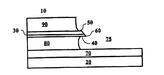
FIG. 1 shows a cross-sectional side elevation view of the electron field
emitter device
10, made on a substrate 20. A emitter 30 consists of an emitting portion 40
and a
gettering portion 50. Emitting portion 40 is a thin layer of a substance with
a low
work function, preferably parallel to substrate 20 to form part of a lateral
field emitter.
Gettering portion 50 is a thin layer of a gettering substance disposed at
least partially
contiguous to emitting portion 40, preferably parallel to substrate 20 and to
emitting
portion 40. Lettering portion 50 acts both as a low-resistance electrical
conductor
and as a gettering surface. Emitting portion 40 and gettering portion 50
together form
an integrated self gettering electron field emitter 30. Emitter 30 has an
extremely fine
i o emitting tip 60. An anode 70 is spaced apart from emitter 30. When anode
70 is
suitably biased positively with respect to emitter 30 to create a high
electric field at
emitting tip 60, electrons emitted from emitting tip 60 in accordance with the
Fowler-
Nordheim equation are attracted to anode 70. Thus anode 70 receives electrons
emitted from emitter 30's emitting tip 60, or more specifically from emitting
portion
15 40. If anode 70 is formed with at least its surface consisting of a
cathodoluminescent
phosphor substance, light is emitted from anode 70 when excited by the
electrons.
Anode 70 may consist entirely of a conductive phosphor. Emitter 30 is
preferably
insulated from anode 70 by an insulating layer 80. Emitter 30 is also
preferably
covered by another insulating layer 90. The preferred structure shown in FIG.
1 is a
20 lateral-emitter device, in which field emitter 30 extends laterally,
parallel to substrate
20.
Because electron field emission in accordance with the Fowler-Nordheim
equation is
very sensitive not only to the radius but also to the work function of fine
emitting tip
60, the emitting portion 40 of emitter 30 preferably has a low work function.
Many
25 known materials are suitable for emitting portion 40. The refractory
transition metals,
such as titanium, zirconium. hafnium, vanadium, niobium, tantalum, chromium,
molybdenum. or tungsten, may be used. Field emitter tips have also been made
from
silicon, carbon (especially in the form of diamond), lanthanum hexaboride, and
other
materials. In the structure of the present invention, emitting portion 40 is
preferably
CA 02312845 2000-06-O1
WO 99/31698 PCT/US98126379
made of a nitrided form of the transition metals listed above, most preferably
nitrided
titanium, nitrided tantalum, or nitrided molybdenum. For some applications, an
alternative embodiment may be used, having emitting portion 40 made of diamond
(carbon having a diamond crystal structure), doped with one or more N-type
dopants
to provide a low work function emitter.
A very important feature of the preferred structure shown in FIG. 1 is the
location of
Bettering portion 50 as close as possible to emitting portion 40 of the
integrated
emitter structure 30, and especially as close as possible to emitting tip 60.
Gettering
portion 50 is made of a substance capable of Bettering undesirable gases which
could
contaminate emitting portion 40. Preferably the Bettering material should be a
substance reactive to the contaminant substances.
Many substances known to be generally useful for Bettering are listed in
references,
t 5 including the following: the chapter "Getters" by E. P. Bertin in "The
Encyclopedia
of Chemistry" 2nd edition (G. L. Clark et al. eds.) ReinhoId Publishing, New
York
( 1966), pp. 484-485; the book by S. Dushman, "Scientific Foundations of
Vacuum
Technique" 2nd edition, John Wiley & Sons, New York (1962) pp. 174-175; and
Chapter 18, "Getter Materials" in W. H. Kohl, "Handbook of Materials and
2o Techniques for Vacuum Devices" Reinhoid Publishing, New York (1967) pp. 545-
562. Substances discussed in these references include aluminum, barium,
beryllium,
calcium, cerium, copper, cobalt, iron, the lanthanide elements, magnesium,
misch
metal, nickel, palladium, thorium, uranium, zinc, titanium, zirconium,
hafnium,
vanadium, niobium, tantalum, chromium, molybdenum, tungsten, and their
suitable
25 alloys, combinations, and mixtures. In general, any of these or other known
getterinB
substances may be used for Bettering portion 50 of emitter 30. The preferred
materials for Bettering portion 50 are the refractory transition metals
titanium,
zirconium, hafrtium, vanadium, niobium, tantalum, chromium, molybdenum,
tungsten, and their alloys, combinations, and mixtures (most preferably
zirconium;).
I1
CA 02312845 2000-06-O1
WO 99/31698 PCT/US98/26379
It is worth noting that there is some advantage to using a transition metal in
its pure
form as a gettering portion 50, integrated with the nitrided form of that same
metal as
the emitting portion 40. During fabrication the nitrided form and the pure
form of the
metal can be deposited sequentially by suitably introducing or withholding
nitrogen.
However, particular applications of the device may influence the choice of
materials.
A preferred nitrided metal used for emitting portion 40 due to other
considerations,
such as work function, may result in a different metal included in gettering
portion 50.
Thus, if the preferred refractory transition metals and their nitrided forms
are used,
those may be of the same metal or different metals. The preferred combinations
are
1o zirconium for gettering portion 50 and nitrides of titanium, tantalum,
molybdenum, or
their mixtures or alloys for emitting portion 40.
FIG. 2 shows a cross-sectional side elevation view of emitting tip 60. Emitter
30
preferably has a tapered edge which determines the shape of emitting tip 60.
~ 5 Emitting tip 60 is preferably made by forming the gettering portion 50
with an edge
55 and forming the emitting portion 40 with a salient part 45 extending beyond
the
edge 55 of the gettering portion to form emitting tip 60. While FIG. 1 shows
anode
70 near the bottom of the final structure (as it typically would be if it were
a phosphor
for display applications), this arrangement is for illustrative purposes only.
Similarly,
2o FIGS. 1 and 2 show the emitting portion 40 of emitter 30 below gettering
portion 50,
but this arrangement is also only illustrative. The reverse order of these
layers (or
other spatial arrangements preserving the contiguous relationship of the
gettering and
emitting portions) would also be functional. An overall device structure such
as the
structure shown in FIG. I and an emitting tip structure like that of FIG. ?
are formed
25 in the preferred fabrication process described in detail below.
12
CA 02312845 2000-06-O1
WO 99/31698 PCT/US98/26379
Preferred Fabrication Process
FIG. 3 shows a flow diagram illustrating steps of a preferred fabrication
process, and
FIGS. 4a - 4e show a sequence of cross-sectional side elevation views of the
device at
various stages during its fabrication. Process steps are denoted by reference
numerals
Sl, S2, ... , S6.
An overall fabrication process includes the steps of providing a substrate,
disposing
an integrated emitter with an emitter layer and a gettering layer parallel to
the
substrate, etching through the emitter layer and Bettering layer to form an
emitting
1 o edge on the integrated emitter, disposing an anode spaced apart from the
emitting
edge for receiving electrons to be emitted from the emitting edge, and
providing
means for applying a suitable electrical bias voltage to the emitter and
anode. In
practice, additional steps typically provide for insulating layers as well:
Steps of the
preferred process are described in detail in the following paragraphs,
referring to FIG.
~5 3 and FIGS. 4a - 4e.
In step Sl, a suitable substrate 20, such as silicon, silicon oxide, silicon
nitride, glass,
or sapphire, is provided. In step S2, an anode layer 70 is deposited on the
substrate
(FIG. 4a) and is optionally patterned. If all the field emission devices on
the substrate
Zo are to share a common anode, no patterning is needed. The optional substep
of
patterning is not shown in the drawings. In general, anode layer 70 may be
made of
any suitable conductive material, deposited in a suitable thickness (e.g. 100
nanometers). For display applications, at least the surface of anode layer 70
should be
a cathodoluminescent phosphor. Many cathodoluminescent phosphors having
various
25 properties such as colors of light emission, luminous efficiencies,
stability, etc. are
known in the art. Several suitable phosphors are described in U.S. Pat. Nos.
5,618,216; 5,630,741; x,644, I 88; 5.644,190; and 5,647,998 to Potter, the
entire
disclosure of each of which is incorporated herein by reference. In one
version of the
preferred process, the anode is zinc oxide (Zn0) with an amount of Zn in
excess over
13
CA 02312845 2000-06-O1
WO 99/31698 PCTIUS98/26379
a stoichiometric amount (usually denoted ZnO:Zn), for producing a display
device
emitting green light. In another version of the preferred process, Ta2Zn308
phosphor
is disposed on at least the surface of the anode, for producing a display
device
emitting blue light.
In step S3, an insulating layer 80 of predetermined thickness is deposited,
preferably
parallel to substrate 20 (FIG. 4b), to provide an insulating spacing between
anode
layer 70 and subsequent elements of the device. Insulating layer 80 may be
made of
any suitable insulator compatible with the other steps of the process, such as
silicon
oxide, silicon nitride, aluminum oxide, etc. In the preferred process,
insulating layer
80 is silicon oxide. A preferred thickness is about 500 nanometers.
In the preferred fabrication process, self gettering emitter 30 is made in
situ while
fabricating a microelectronic field emission device. In step S4, the self
gettering
integrated emitter 30 is disposed over insulating layer 80, parallel with
substrate 20
(FIG. 4c). In the most preferred embodiment, step S4 is performed in two
substeps,
S4a and S4b. In substep S4a, an emitting portion 40 is deposited, comprising a
layer
of a substance with low work function for electron emission. In substep S4b, a
gettering portion 50 is deposited, consisting of a layer of a gettering
substance. The
zo thickness of emitting portion 40 is preferably about 10 - 30 nanometers.
The
thickness of gettering portion 50 is preferably about 100 - 200 nanometers.
Various
materials suitable for each of these layers of the emitter are described above
in the
detailed description of the device structure. Deposition of the layers of
emitter 30
may be done by any conventional deposition method suitable to the substance
being
deposited, such as evaporation, chemical vapor deposition, molecular beam
deposition, plating, etc.. instead of the preferred method of sputtering. The
emitter 30
may be patterned in a conventional manner such as in the known
photolithographic
methods commonly used in semiconductor fabrication processes. Such patterning
is
described in the patents of Potter incorporated by reference hereinabove. This
14
CA 02312845 2000-06-O1
WO 99131698 PCTNS98/26379
conventional patterning substep is not shown in the drawings. An important
feature
of the most preferred in situ process is realized when the two portions of the
self
Bettering emitter are based on refractory transition metals: a nitrided
refractory
transition metal deposited as the emitting portion 40 in substep S4a, and a
layer of a
refractory transition metal deposited as the Bettering portion in substep S4b.
The
transition metal basis of these two portions may be different elements or may
be based
on the same element, e.g. nitrided titanium such as TiN as the emitting
portion and
pure titanium for the Bettering portion, both based on titanium. A preferred
example
using different elements has an emitting portion comprising a nitrided form of
to titanium, tantalum, molybdenum, or their mixtures or alloys, and the
Bettering portion
comprises zirconium metal. When the transition metal element is the same in
the two
portions of emitter 30, it is possible to deposit emitter 30 in a continuous
process, by
reactive sputtering of the metal in the presence of nitrogen to form the
nitrided layer
for emitting portion 40, and then by continuing to sputter the metal while
withholding
nitrogen to sputter the pure-metal Bettering portion 50. With such a process,
there is
not necessarily a sharp boundary delineating the two portions 40 and 50; the
nitrogen
content can diminish more or less gradually from a relatively high level at
emitter
portion 40 to a low level, preferably zero, in Bettering portion 50. A similar
gradual
variation of composition may be obtained even with different transition metals
in the
Zo two portions 40 and 50, in cases where the two metals form solid solution
alloys in
the thin films.
While the prefen:ed embodiment described herein has an emitter 30 having two
layers
40 and 50, an alternate embodiment (shown in FIG. 5) has a laminar composite
?5 emitter having three layers: a medial emitting layer 40 and upper and lower
Bettering
layers 50, one Bettering layer above and one Bettering layer below the
emitting layer.
Field emission device structures having three-layer composite lateral emitters
(without
the self Bettering feature) and their fabrication are described in detail in
LT.S. Pat. No.
5,647,998 to Potter, which is incorporated by reference hereinabove.
CA 02312845 2000-06-O1
WO 99!31698 PCT/US98/26379
In step S5, a second insulating layer 90 is optionally deposited over emitter
30 (FIG.
4d). This second insulator may be of the same insulating material as layer 80,
and
may be about 50 - 200 nanometers thick. Silicon oxide is a preferred material.
Insulating layer 90 protects the emitter and may provide an insulating spacer
from the
emitter for any gate electrode disposed above the plane of emitter 30 for
controlling
the electron current flowing from emitter tip 60 to anode 70.
In step S6, a directional etch is performed through second insulating layer 90
if
present, through both emitting layer 40 and gettering layer 50 of emitter 30,
and
o through insulating layer 80, to form emitting edge 60 and to form an opening
75 that
extends down to anode 70 (FIG. 4e). The width of opening 75 is not critical; a
typical
width is about 2 - 20 micrometers. The directional etch is preferably an
anisotropic
"trench" etch such as the reactive ion etching commonly used in semiconductor
fabrication processes. This etching process preferentially etches the
insulating layers
15 80 and 90 relative to its etching of the materials of emitter 30. While
such an etch
process is generally controlled to be highly anisotropic, it is preferably
controlled to
include some degree of isotropic etching in the present application. This
creates the
emitter structure shown in detail in FIG. 2. The etching process of step S6
forms a
thin emitting edge 60 on emitting portion 40 and forms an edge 55 on gettering
2o portion 50 such that a salient portion 45 of the emitting portion 40
extends beyond
edge 55, thus forming emitting tip 60 with the desired shape and self
gettering
property. Since gettering portion 50 has a salient portion extending beyond
the etched
surface of insulating layers 80 and/or 90, the salient portion 45 of the
emitter also
extends beyond the surface of insulating layers 80 and/or 90. The exposed part
of
25 gettering portion 50 is positioned very favorably for gettering
contaminants,
immediately adjacent to emitting tip 60 and to the salient part 45 of emitting
portion
40.
16
CA 02312845 2000-06-O1
WO 99/31698 PCT/US98/26379
The formation of emitting tip 60 is preferably done while forming the trench
opening
75, but may be done after forming that opening. A small amount of the
supporting
upper and/or lower Bettering layers) 50 is removed, for example by etching in
a
plasma etch process. A differential etch process is chosen such that emitting
portion
40 of the laminar emitter is less effected by the etch than the Bettering
portions) 50.
This leaves an ultra thin emitter edge or tip 60. For some combinations of
materials in
the laminar composite emitter 30, a preferred differential etch process may be
a
chemical or electro-chemical etch, differential electropolishing, or
differential
ablation.
to Once the device structure of FIG. 1 is formed, operation of the device
requires means
for applying a suitable electrical bias voltage to the emitter and anode,
sufficient to
cause emission of electrons from the emitter to the anode, in a conventional
manner
for field-emission devices. Thus the completed device has conductive contacts
arranged to allow connection of the appropriate bias voltages from outside the
device.
15 Such conductive contact arrangements are described in the patents of Potter
incorporated by reference hereinabove.
INDUSTRIAL APPLICABILITY
The invention is useful in fabrication of field emission devices and is
especially useful
Zo for field emission displays that consist of an array of field emission
devices, since
each device in the array may have a self Bettering emitter. The preferred
fabrication
process is specially adapted for simultaneous fabrication of many devices in
such an
array. A self Bettering emitter made in accordance with the invention may also
be
used as an electron emitter part of an electron gun structure.
From the foregoing description, one skilled in the art can easily ascertain
the essential
characteristics of this invention, and without departing from the spirit and
scope
thereof, can make various changes and modifications of the invention to adapt
it to
various usages and conditions. Other embodiments of the invention will be
apparent
17
CA 02312845 2000-06-O1
WO 99/31698 PC'T/US98/26379
to those skilled in the art from a consideration of this specification or from
practice of
the invention disclosed herein. For example, the order of steps of the
fabrication
process may be varied, and other suitable materials may be substituted for
those
described herein. While the preferred embodiment of the emitter has been
described
in a structure intended for displays, the self gettering emitter may be made
as an
isolated element, for example by removing the substrate. It is intended that
the
specification and examples be considered as exemplary only, with the true
scope and
spirit of the invention being defined by the following claims.
Having described my invention, I claim:
18