Note: Descriptions are shown in the official language in which they were submitted.
CA 02312958 2000-06-05
V~O 99/30427 PCT/US9846053
PROGRAMMABLE DYNAMIC RANGE RECEIVER
BACKGROUND OF THE INVENTION
I. Field of the Invention
The present invention relates to communications. More particularly,
the present invention relates to a novel and improved programmable
dynamic range receiver.
II. Description of the Related Art
The design of a high performance receiver is made challenging by
various design constraints. First, high performance is required for many
applications. High performance can be described by the linearity of the
active devices (e.g. amplifiers, mixers, etc.) and the noise figure of the
receiver. Second, for some applications such as in a cellular communication
system, power consumption is an important consideration because of the
portable nature of the receiver. Generally, high performance and high
efficiency are conflicting design considerations.
An active device has the following transfer function:
y(x) = a, = x+ a2= x2 + a3 = x3 + higher order terms (1)
where x is the input signal, y(x) is the output signal, and al, az, and a3 are
coefficients which define the linearity of the active device. For simplicity,
higher order terms (e.g; terms above third order) are ignored. For an ideal
active device, the coefficients a2 and a3 are 0.0 and the output signal is
simply the input signal scaled by al. However, all active devices experience
some amount of non-linearity which is quantified by the coefficients a2 and
a3. Coefficient a2 defines the amount of second order non-linearity and
coefficient a3 defines the amount of third order non-linearity.
Most communication systems are narrow band systems which operate
on an input RF signal having a predetermined bandwidth and center
frequency. The input RF signal typically comprises other spurious signals
located throughout the frequency spectrum. Non-linearity within the active
devices causes intermodulation of spurious signals, resulting in products
which may fall into the signal band.
CA 02312958 2000-06-05
WO 99/30427 2 PCT/US9846053
The effect of second order non-linearity (e.g. those caused by the x2
term) can usually be reduced or eliminated by careful design methodology.
Second order non-linearity produces products at the sum and difference
frequencies. Typically, the spurious signals which can produce in-band
second-order products are located far away from the signal band and can be
easily filtered. However, third order non-linearity are more problematic.
For third order non-linearity, spurious signals x = gl=cos(wlt) + g2=cos(w2t)
produce products at the frequencies (2w1-w2) and (2w2-wl). Thus, near band
spurious signals (which are difficult to filter) can produce third order
intermodulation products falling in-band, causing degradation in the
received signal. To compound the problem, the amplitude of the third-
order products are scaled by gl=g2 and g12=g2. Thus, every doubling of the
amplitude of the spurious signals produces an eight-fold increase in the
amplitude of the third order products. Viewed another way, every 1 dB
increase in the input RF signal results in 1 dB increase in the output RF
signal but 3 dB increase in the third order products.
The linearity of a receiver (or the active device) can be characterized
by the input-referred third-order intercept point (IIP3). Typically, the
output
RF signal and the third-order intermodulation products are plotted versus
the input RF signal. As the input RF signal is increased, the IIP3 is a
theoretical point where the desired output RF signal and the third-order
products become equal in amplitude. The IIP3 is an extrapolated value since
the active device goes into compression before the IIP3 point is reached.
For a receiver comprising multiple active devices connected in
cascade, the IIP3 of the receiver from the first stage of active device to the
nth
stage can be calculated as follows :
IIP3õ = -10- 1og40-Ap V,J10+lO(AvR-MP3e.)i1o11 (2)
where IIP3n is the input-referred third-order intercept point from the first
stage of active device to the nth stage, IIP3n_i is the input-referred third-
order
intercept point from the first stage to the (n-1) th stage, Avn is the gain of
the
nth stage, IIP3dn is the input-referred third-order intercept point of the nth
stage, and all terms are given in decibel (dB). The calculation in equation
(2)
can be carried out in sequential order for subsequent stages within the
receiver.
CA 02312958 2000-06-05
WO 99/30427 PCT/US98J26053
3
From equation (2), it can be observed that one way to improve the
cascaded IIP3 of the receiver is to lower the gain before the first non-linear
active device. However, each active device also generates thermal noise
which degrades the signal quality. Since the noise level is maintained at a
constant level, the degradation increases as the gain is lowered and the
signal amplitude is decreased. The amount of degradation can be measured
by the noise figure (NF) of the active device which is given as follows :
NFd = SNRõ - SNP... (3)
where NFd is the noise figure of the active device, SNRiII is the signal-to-
noise ratio of the input RF signal into the active device, SNRout is signal-to-
noise ratio of the output RF signal from the active device, and NFd, SNRin
and SNRout are all given in decibel (dB). For a receiver comprising multiple
active devices connected in cascade, the noise figure of the receiver from the
first stage of active device to the nei stage can be calculated as follows :
r (NF., /lC) 10(NF, /10) - 11
NFõ =10 = 1og101 10 + 1joy(c- /10) 1
, (4)
where NFn is the noise figure from the first stage to the nt' stage, NFn_i is
the
noise figure of the first stage to the (n-1)th stage, NFd, is the noise figure
of
the nth stage, and Gn_1 is the accumulated gain of the first stage through the
(n-1)ei stage in dB. As shown in equation (4), the gain of the active device
can affect the noise figure of the subsequent stages. Similar to the IIP3
calculation in equation (2), the noise figure calculation in equation (4) can
be
carried out in sequential order for subsequent stages of the receiver.
Receivers are employed for many communication applications, such
as cellular communication systems and high definition television (HDTV).
Exemplary cellular communication systems include Code Division Multiple
Access (CDMA) communication systems, Time Division Multiple Access
(TDMA) communication systems, and analog FM communication systems.
The use of CDMA techniques in a multiple access communication system is
disclosed in U.S. Patent No. 4,901,307, entitled "SPREAD SPECTRUM
MULTIPLE ACCESS COMMUNICATION SYSTEM USING SATELLITE OR
TERRESTRIAL REPEATERS", and U.S. Patent No. 5,103,459, entitled
"SYSTEM AND METHOD FOR GENERATING WAVEFORMS IN A CDMA
CA 02312958 2003-12-12
74769-261
4
CELLULAR TELEPHONE SYSTEM", both assigned to the assignee of
the present invention. An exemplary HDTV system is
disclosed in U.S. Patent No. 5,452,104, U.S. Patent No.
5,107,345, and U.S. Patent No. 5,021,891, all three entitled
"ADAPTIVE BLOCK SIZE IMAGE COMPRESSION METHOD AND SYSTEM",
and U.S. Patent No. 5,576,767, entitled "INTERFRAME VIDEO
ENCODING AND DECODING SYSTEM", all four patents assigned to
the assignee of the present invention.
In cellular applications, it is common to have
more than one communication system operating within the same
geographic coverage area. Furthermore, these systems can
operate at or near the same frequency band. When this
occurs, the transmission from one system can cause
degradation in the received signal of another system. CDMA
is a spread spectrum communication system which spreads the
transmit power to each user over the entire 1.2288 MHz
signal bandwidth. The spectral response of an FM-based
transmission can be more concentrated at the center
frequency. Therefore, FM-based transmission can cause
jammers to appear within the allocated CDMA band and very
close to the received CDMA signal. Furthermore, the
amplitude of the jammers can be many time greater than that
of the CDMA signal. These jammers can cause third-order
intermodulation products which can degrade the performance
of the CDMA system.
Typically, to minimize degradation due to
intermodulation products caused by jammers, the receiver is
designed to have high IIP3. However, design of a high IIP3
receiver requires the active devices within the receiver to
be biased with high DC current, thereby consuming large
amounts of power. This design approach is especially
CA 02312958 2003-12-12
74769-261
undesirable for cellular application wherein the receiver is
a portable unit and power is limited.
Several techniques have been deployed in the prior
art to address the need for high IIP3. One such technique,
5 which also attempts to minimize power consumption, is to
implement the gain stage with a plurality of amplifiers
connected in parallel and to selectively enable the
amplifiers as higher IIP3 is needed. This technique is
disclosed in detail in U.S. Patent No. 6,069,525 issued May
30, 2000, entitled "DUAL MODE AMPLIFIER WITH HIGH EFFICIENCY
AND HIGH LINEARITY", assigned to the assignee of the present
invention. Another technique is to measure the received RF
signal power and adjust the gain of the amplifiers based on
the amplitude of the RF signal power. This technique is
disclosed in detail in U.S. Patent No. 5,722,061 issued
February 24, 1998, entitled "METHOD AND APPARATUS FOR
INCREASING RECEIVER POWER IMMUNITY TO INTERFERENCE", filed
September 30, 1996 assigned to the assignee of the present
invention. These techniques improve the IIP3 performance
but have not effectively reduced power consumption nor
minimized circuit complexity.
An exemplary block diagram of a receiver
architecture of the prior art is shown in FIG. 1. Within
receiver 1100, the transmitted RF signal is received by
antenna 1112, routed through duplexer 1114, and provided to
low noise amplifier (LNA) 1116. LNA 1116 amplifies the RF
signal and provides the signal to bandpass filter 1118.
Bandpass filter 1118 filters the signal to remove some of
the spurious signals which can cause intermodulation
products in the subsequent stages. The filtered signal is
provided to mixer 1120 which downconverts the signal to an
intermediate frequency (IF) with the sinusoidal from local
CA 02312958 2003-12-12
74769-261
6
oscillator 1122. The IF signal is provided to bandpass
filter 1124 which filters spurious signals and
downconversion products prior to the subsequent
downconversion stage. The filtered IF signal is provided to
automatic-gain-control (AGC) amplifier 1126 which amplifies
the signal with a variable gain to provide an IF signal at
the required amplitude. The gain is controlled by a control
signal from AGC control circuit 1128. The IF signal is
provided to demodulator 1130 which demodulates the signal in
accordance with the modulation format used at the
transmitter. For digital transmission such as binary phase
shift keying (BPSK), quaternary phase shift keying (QPSK),
offset quaternary phase shift keying (OQPSK), and quadrature
amplitude modulation (QAM), a digital demodulator is used to
provide the digitized baseband data. For FM transmission,
an FM demodulator is used to provide the analog signal.
Receiver 1100 comprises the basic functionalities
required by most receivers. However, the location of
amplifiers 1116 and 1126, bandpass filters 1118 and 1124,
and mixer 1120 can be rearranged to optimize the receiver
performance for a particular application. In this receiver
architecture, high IIP3 is provided for by biasing the
active devices at high DC bias current and/or by controlling
the gain of amplifier 1126.
This receiver architecture has several drawbacks.
First, the active devices are typically biased to a high DC
current to provide the highest required IIP3. This has the
effect of operating receiver 1100 at the high IIP3 operating
point at all times, even though high IIP3 is not required
most of the time. Second, the high IIP3 can be improved by
CA 02312958 2003-12-12
74769-261
6a
adjusting the gain of AGC amplifier 1126, as disclosed in
the aforementioned U.S. Patent No. 5,099,204. However,
lowering the gain of amplifier 1126 can degrade the noise
figure of receiver 1100.
SUMMARY OF THE INVENTION
The present invention is a novel and improved
programmable dynamic range receiver which provides the
requisite level of performance with reduced power
consumption. In the exemplary embodiment, the receiver
comprises a front end, a EA ADC, a digital signal processor,
a power detector, and an AGC control circuit. In the
exemplary embodiment, the input RF signal is conditioned and
downconverted into an IF signal by the front end. The IF
signal is quantized by the EA ADC to produce IF samples
which are processed by the digital signal processor to yield
the desired signal. The power detector measures the
amplitude of the signal into the EA ADC. In the exemplary
embodiment, the required dynamic range is computed from
measurement of the amplitude of the desired signal and the
signal into the EA ADC. In the alternative embodiment, the
required dynamic range is determined based on the operating
mode of the receiver.
The invention may be summarized according to a
first broad aspect as a programmable dynamic range receiver
comprising: a front end for receiving an RF signal and
producing an IF signal; a EA ADC connected to said front end
for receiving said IF signal and producing IF samples, said
EA ADC having a dynamic range; a power detector connected to
said front end for measuring an amplitude of said IF signal;
and a digital signal processor connected to said EA ADC for
receiving said IF samples and producing a desired signal;
CA 02312958 2003-12-12
74769-261
6b
wherein said dynamic range of said EA ADC is adjusted based
on a required dynamic range, said required dynamic range
dependent on said amplitude of said IF signal.
According to a second broad aspect the invention
provides a method for providing programmable dynamic range
in a receiver comprising the steps of: receiving an RF
signal; processing said RF signal to produce an IF signal;
sampling said IF signal with a EA ADC to produce IF samples,
said EA ADC having a dynamic range; processing said IF
samples to produce a desired signal; measuring an amplitude
of said IF signal; measuring an amplitude of said desired
signal; computing a required dynamic range in accordance
with said measured amplitude of said IF signal and said
measured amplitude of said desired signal; and adjusting
said dynamic range of said EA ADC in accordance with said
required dynamic range.
It is an object of the present invention to
provide a programmable dynamic range receiver which
minimizes power consumption by enabling and disabling one or
more loops within the EA ADC. In the exemplary embodiment,
the EA ADC is implemented with one or more loops. Each loop
provides a predetermined dynamic range performance. One or
more loops within the EA ADC can be enabled or disabled as
the required dynamic range exceeds or falls below a set of
dynamic range thresholds. The dynamic range thresholds can
be selected based on numerous considerations, such as the
statistics of the input RF signal and the performance of the
EA ADC. Furthermore, the dynamic range thresholds can be
implemented with hysteresis to prevent toggling of the loops
between the enabled and disabled states.
CA 02312958 2003-12-12
74769-261
6c
It is another object of the present invention to
provide a programmable dynamic range receiver which
minimizes power consumption by adjustment of the bias
current. In the exemplary embodiment, the EA ADC is
designed with adjustable bias current. The dynamic range of
the EA ADC varies approximately proportional to the bias
current. By adjusting the bias current, the required
dynamic range can be provided by the EA ADC with minimal
power consumption. The bias current can be adjusted in
discrete steps or in continuous manner.
CA 02312958 2000-06-05
WO 99/30427 PGT/US98/26053
7
It is yet another object of the present invention to provide a
programmable dynamic range receiver which minimizes power
consumption by adjustment of a reference voltage on the EO ADC. The
dynamic range of the EA ADC is determined by the maximum input signal
swing and the noise from LA ADC which comprises the circuit noise and the
quantization noise. As the required dynamic range decreases, the reference
voltage can be lowered while maintaining approximately the same noise
level. This is especially true when one loop is switched out and the
quantization noise increases such that it is much greater than the circuit
noise. By lowering the reference voltage such that the quantization noise is
approximately equal to the circuit noise, the desired level of performance is
provided while maintaining the signal level at a low level. As an additional
benefit, the amplifier driving the MA ADC has a lower maximum signal
swing and can be biased with less current.
It is yet another object of the present invention to provide a
programmable dynamic range receiver which minimizes power
consumption by adjustment of the sampling frequency of the MA ADC. The
dynamic range of the F,A ADC is a function of the oversampling ratio which
is proportional to the sampling frequency, since the bandwidth of the signal
into the MA ADC is constant. High dynamic range requires a high
oversampling ratio. The power consumption of the circuits used to
implement the LA ADC can be dependent on the sampling frequency. In the
present invention, when high dynamic range is not required, the sampling
frequency can be lowered to minimize power consumption.
It is yet another object of the present invention to provide a
programmable dynamic range receiver which minimizes power
consumption by switching on the appropriate FA ADC based on the required
performance. In this embodiment, the receiver can be designed with two or
more EA ADCs which provide the sampling function for two or more
operating modes. For example, a receiver can be designed with two MA
ADCs, one for CDMA mode and one for FM mode. The MA ADC for the FM
mode can be designed to consume significantly less power because of the
lower signal bandwidth and the lower required dynamic range. The
appropriate LA ADC can be switched on depending on whether the receiver
is operating in the CDMA or FM mode.
The features described above can be combined, as appropriate, to
provide the required level of performance while maximizing power
savings.
CA 02312958 2000-06-05
WO 99/30427 8 PCT/US98/26053
BRIEF DESCRIPTION OF THE DRAWINGS
The features, objects, and advantages of the present invention will
become more apparent from the detailed description set forth below when
taken in conjunction with the drawings in which like reference characters
identify correspondingly throughout and wherein:
FIG. 1 is a block diagram of an exemplary receiver of the prior art;
FIG. 2 is a block diagram of an exemplary programmable linear
receiver of the present invention;
FIG. 3 is a block diagram of an exemplary programmable linear dual-
band receiver of the present invention;
FIG. 4 is a block diagram of an exemplary QPSK demodulator which is
used within the receivers of the present invention;
FIG. 5A-5B are schematic diagrams of an exemplary discrete design of
low-noise-amplifier (LNA) and current source which are used in the
receivers of the present invention, respectively;
FIG. 6A-6B are diagrams of the IIP3 performance versus bias current of
the transistor used in the LNA and the performance curves of the LNA,
respectively;
FIG. 7A-7B are diagrams of the two-tone and single-tone jammers
specifications for CDMA signal as defined by IS-98-A, respectively;
FIG. 8A-8B are diagrams of the AGC control range for ascending and
descending CDMA input power, respectively;
FIG. 9 is a diagram of an exemplary IIP3 bias control mechanism of the
present invention;
FIG. 10A-10B are diagrams of the IIP3 bias control for ascending and
descending CDMA input power, respectively; and
FIG.11 is a block diagram of an exemplary two loop bandpass MASH
F.A analog-to-digital converter.
DETAILED DESCRIPTION OF THE PREFERRED
EMBODIMENTS
The receiver of the present invention provides the requisite level of
system performance and minimizes power consumption by controlling the
DC bias of the active devices. The present invention can be practiced using
CA 02312958 2000-06-05
WO 99/30427 PCT/US982603
9 -
one of three embodiments described in detail below. In the first
embodiment, the amount of non-linearity at the output of the receiver is
measured and used to set the IIP3 operating point of the active devices
within the receiver, such as the amplifiers and mixer. In the second
embodiment, the 11P3 operating point of the active devices are set in
accordance with the expected received signal level based on the operating
mode of the receiver. And in the third embodiment, the IIP3 operating
point of the active devices are set in accordance with the measured signal
level at various stages within the receiver.
In the present invention, the AGC function is provided by an AGC
control circuit which operates in conjunction with a bias control circuit. The
IIP3 operating point of the active devices are set in accordance with the
measured amount of non-linearity which is dependent on the amplitude of
the signal. The signal amplitude, in turn, depends on the gain settings of
the receiver. In the present invention, the AGC and bias control are
operated in an integrated manner to provide the required level of linearity
over a specified AGC range while minimizing power consumption.
L Receiver Architecture
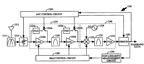
A block diagram of an exemplary receiver architecture of the present
invention is shown in FIG. 2. Within receiver 1200, the transmitted RF
signal is received by antenna 1212, routed through duplexer 1214, and
provided to attenuator 1216. Attenuator 1216 attenuates the RF signal to
provide a signal at the required amplitude and provides the attenuated
signal to RF processor 1210. Within RF processor 1210, the attenuated signal
is provided to pad 1222a and low noise amplifier (LNA) 1220a. LNA 1220a
amplifies the RF signal and provides the amplified signal to bandpass filter
1226. Pad 1222a provides a predetermined level of attenuation and connects
in series with switch 1224a. Switch 1224a provides a bypass route around
LNA 1220a when the gain of LNA 1220a is not needed. Bandpass filter 1226
filters the signal to remove spurious signals which can cause
intermodulation products in the subsequent signal processing stages. The
filtered signal is provided to pad 1222b and low noise amplifier (LNA) 1220b.
LNA 1220b amplifies the filtered signal and provides the signal to RF/IF
processor 1248. Pad 1222b provides a predetermined level of attenuation and
connects in series with switch 1224b. Switch 1224b provides a bypass route
around LNA 1220b when the gain of LNA 1220b is not needed. Within
CA 02312958 2003-12-12
747=69-261
RF/IF processor 1248, mixer 1230 downconverts the signal to
an intermediate frequency (IF) with the sinusoidal from
local oscillator (LO) 1228. The IF signal is provided to
bandpass filter 1232 which filters out spurious signals and
5 out-of-band downconversion products. In the preferred
embodiment, the filtered IF signal is provided to voltage
control amplifier (VGA) 1234 which amplifies the signal with
a variable gain which is adjusted by a gain control signal.
Amplifier 1234 can also be implemented as a fixed gain
10 amplifier, depending on the system requirement, and this is
also within the scope of the present invention. The
amplified IF signal is provided to demodulator 1250 which
demodulates the signal in accordance with the modulation
format used by the transmitter (not shown). RF processor
1210 and RF/IF processor 1248 is collectively referred to as
a front end.
A block diagram of an exemplary demodulator 1250
used for demodulation of quadrature modulated signals (e.g.
QPSK, OQPSK, and QAM) is illustrated in FIG. 4. In the
exemplary embodiment, demodulator 1250 is implemented as a
subsampling bandpass demodulator. The IF signal is provided
to bandpass sigma delta analog-to-digital converter (EO ADC)
1410 which quantizes the signal at a high sampling frequency
determined by the CLK signal. An exemplary design of a
ED ADC is described in detail in U.S. Patent No. 5,982,315
issued November 9, 1999 entitled "SIGMA-DELTA ANALOG-TO-
DIGITAL CONVERTER", and assigned to the assignee of the
present invention. The use of a ED ADC within a receiver is
disclosed in copending U.S. Patent No. 6,005,506 issued
December 21, 1999 entitled "RECEIVER WITH SIGMA-DELTA
CA 02312958 2003-12-12
74769-261
l0a
ANALOG-TO-DIGITAL CONVERTER", assigned to the assignee of
the present invention. The quantized signal is provided to
filter 1412 which filters and decimates the signal. The
filtered signal is provided to multipliers 1414a and 1414b
which downconvert the signal to baseband with the in-phase
and quadrature sinusoids from local oscillator (L02) 1420
and phase shifter 1418, respectively. Phase shifter 1418
provides 90 of phase shift for the quadrature sinusoidal.
The baseband I and Q signals are provided to lowpass filters
1416a and 1416b, respectively, which filter the signal to
provide the I and Q data. The baseband data in FIG. 2
comprises the I and Q data in FIG. 4. In the exemplary
embodiment, filter 1412 and/or lowpass filters 1416 also
provide scaling of the signal to enable demodulator 1250 to
provide baseband data at various amplitudes. Other
implementations of
CA 02312958 2000-06-05
WO 99/30427 11 PCT/US98/26053
demodulator 1250 can be designed to performed the demodulation of QPSK
modulated waveform and are within the scope of the present invention.
Referring back to FIG. 2, receiver 1200 comprises the basic
functionalities required by most receivers. However, the arrangement of
attenuator 1216, LNAs 1220a and 1220b, bandpass filters 1226 and 1232, and
mixer 1230 can be reordered to optimize the performance of receiver 1200 for
specific applications. For example, attenuator 1216 can be interposed
between LNA 1220a and bandpass filter 1226 to improve the noise figure
performance. Furthermore, a bandpass filter can be inserted before LNA
1220a to remove undesirable spurious signals before the first amplifier stage.
Different arrangements of the functionalities shown herein can be
contemplated and are within the scope of the present invention.
Furthermore, other arrangements of the functionalities shown herein in
combination with other receiver functionalities which are known in the art
can also be contemplated and are within the scope of the present invention.
In the present invention, attenuator 1216, switches 1224a and 1224b,
and demodulator 1250 are controlled by AGC control circuit 1260 such that
the IF signal from amplifier 1234 is at the required amplitude. The AGC
function is described in detail below. In the exemplary embodiment, LNAs
1220a and 1220b are fixed gain amplifiers. LNAs 1220a and 1220b and mixer
1230 are controlled by bias control circuit 1280 to adjust the DC bias current
and/or voltages of these active devices such that the required linearity
performance is achieved with minimal power consumption. The variable
IIP3 bias control mechanism is described in detail below.
The receiver architecture of the present invention can be adopted for
use in various applications, including cellular telephone and HDTV
applications. In the cellular telephone, receiver 1200 can be adopted for use
in CDMA communication systems operating at the personal
communication system (PCS). band or the cellular band.
A block diagram of an exemplary receiver which supports dual-band
(PCS and cellular) and dual-mode (CDMA and AMPS) is shown in FIG. 3.
The PCS band has a bandwidth of 60 MHz and a center frequency of
1900 MHz. The cellular band has a bandwidth of 25 MHz and a center
frequency of 900 MHz. Each band requires a unique RF bandpass filter.
Therefore, two RF processors are used for the two bands.
Receiver 1300 comprises many of the same components as those i n
receiver 1200 (see FIG. 2). Antenna 1312, duplexer 1314, and attenuator 1316
are identical to antenna 1212, duplexer 1214, and attenuator 1216 in receiver
1200. The attenuated signal from attenuator 1316 is provided to RF
CA 02312958 2000-06-05
WO 99/30427 PCT/US98R6053
12
processors 1310a and 1310b. RF processor 1310a is designed to operate at the
cellular band and RF processor 1310b is designed to operate at the PCS band.
RF processor 1310a is identical to RF processor 1210 in receiver 1200. RF
processor 1310a comprises two stages of low-noise amplifier (LNA) 1320a
and 1320b connected in cascade with bandpass filter 1326 interposed between
the stages. Each LNA 1320 has a parallel signal path comprising pad 1322
and switch 1324. RF processor 1310b is similar to RF processor 1310a except
that LNAs 1321a and 1321b and bandpass filter.1327 are designed to operate at
the PCS band. The output from RF processors 1310a and 1310b are provided
to multiplexer (MUX) 1346 which selects the desired signal in accordance
with a control signal from controller 1370 (not shown in FIG. 3 for
simplicity). The RF signal from MUX 1346 is provided to RF/IF processor
1348 which is identical to RF/IF processor 1248 in FIG. 2. The IF signal from
processor 1348 is provided to demodulator (DEMOD) 1350 which
demodulates the signal in accordance with the modulation format used at
the remote transmitter (not shown). Demodulator 1350, AGC control circuit
1360, bias control circuit 1380, and non-linearity measurement circuit 1390 in
FIG. 3 are identical to demodulator 1250, AGC control circuit 1260, bias
control circuit 1280, and non-linearity measurement circuit 1290 in FIG. 2,
respectively.
Controller 1370 connects to AGC control circuit 1360, bias control
circuit 1380, and MUX 1346 and controls the operation of these circuits.
Controller 1370 can be implemented as a microprocessor, a microcontroller,
or a digital signal processor programmed to perform the functions herein
described. Controller 1370 can also comprise a memory storage element for
storing the operating modes of receiver 1300 and the associated control
signals.
Referring to FIG. 2, an exemplary design of receiver 1200 especially
adopted for cellular telephone application is given in detail below. In the
exemplary embodiment, attenuator 1216 has an attenuation range of 20 dB
and provides an attenuation of 0.2 dB to -20 dB. Attenuator 1216 can be
designed with a pair of diodes or by field effect transistors (FETs), the
implementations of which are known in the art. In the exemplary
embodiment, LNAs 1220a and 1220b have fixed gains of 13 dB each. LNAs
1220a and 1220b can be off-the-shelf monolithic RF amplifiers or amplifiers
designed using discrete components. An exemplary discrete design of LNA
1220 is given in detail below. In the exemplary embodiment, pads 1222a and
1222b provide 5 dB of attenuation and can be implemented with resistors in
the manner known in the art. In the exemplary embodiment, bandpass
CA 02312958 2003-12-12
747=69-261
13
filter 1226 is a surface acoustic wave (SAW) filter which
has a bandwidth of 25 MHz, the entire bandwidth of the
cellular band, and is centered about 900 MHz.
In the exemplary embodiment, bandpass filter 1232
is also a SAW filter which has a bandwidth of 1.2288 MHz,
the bandwidth of one CDMA system, and is centered about
116.5 MHz. Mixer 1230 is an active mixer which can be an
off-the-shelf mixer, such as the Motorola MC13143, or other
active mixer which is designed in the manner known in the
art. Mixer 1230 can also be implemented with passive
components, such as double-balanced diode mixer. Amplifier
1234 can be a monolithic amplifier or an amplifier designed
with discrete components. In the exemplary embodiment,
amplifier 1234 is designed to provide a gain of 40 dB.
In the exemplary embodiment, the overall gain
range of receiver 1200, excluding demodulator 1250, is
+51 dB to -5 dB. This gain range presumes exemplary
insertion loss of -3 dB for bandpass filter 1226, gain of
+1 dB for mixer 1230, and insertion loss of -13 dB for
bandpass filter 1232. For CDMA applications, an AGC range
of 80 dB is typically required to adequately handle path
loss, fading conditions, and jammers. In the exemplary
embodiment, the AGC range provided by attenuator 1216, LNAs
1220a and 1220b, and pads 1222a and 1222b is 56 dB. In the
exemplary embodiment, the remaining 24 dB of AGC range is
provided by demodulator 1250 and/or amplifier 1234. Within
demodulator 1250 (see FIG. 4), ADC 1410 quantizes the analog
waveform and provides the digitized values to the subsequent
digital signal processing blocks. In the exemplary
embodiment, the required resolution for ADC 1410 is four
CA 02312958 2003-12-12
747=69-261
13a
bits. In the exemplary embodiment, an additional six bits
of resolution provides headroom for the yet unfiltered
jammers. ADC 1410 can be designed to provide more than ten
bits of resolution. Each additional bit over ten can be
used to provide 6 dB of gain control. Fortunately, at high
CDMA signal levels, the out-of-band jammer levels cannot
continue to be +72 dB above the CDMA signal. Therefore,
when the CDMA signal is strong, the jammers require less
than 6 bits of resolution for jammer headroom. In the
exemplary embodiment, the AGC function performed in
demodulator 1250 is active only when the CDMA signal is
strong, e.g., at the high end of the CDMA control range.
Thus, the extra bits of resolution which are initially
reserved for jammer headroom are now used for the AGC
function as the result of the strong CDMA signal levels.
The design of a subsampling bandpass EA ADC which provides
the performance required for receiver 1200 is disclosed in
the aforementioned copending U.S. Patent No. 6,005,506.
CA 02312958 2000-06-05
WO 99/30427 PCT/US98/26053
14
II. Amplifier Design
A schematic diagram of an exemplary discrete LNA design is shown
in FIG. 5A. Within LNA 1220, the RF input is provided to one end of AC
coupling capacitor 1512. The other end of capacitor 1512 connects to one end
of capacitor 1514 and inductor 1516. The other end of capacitor 1514 connects
to analog ground and the other end of inductor 1516 connects to one end of
resistors 1518 and 1520 and the base of transistor 1540. The other end of
resistor 1518 connects to the power supply Vdc and the other end of resistor
1520 connects to analog ground. Bypass capacitor 1522 connects to Vdc and
analog ground. In the exemplary embodiment, transistor 1540 is a low noise
RF transistor, such as the Siemens BFP420, which is commonly used in the
art. The emitter of transistor 1540 connects to one end of inductor 1542. The
other end of inductor 1542 connects to current source 1580 which also
connects to analog ground. The collector of transistor 1540 connects to one
end of inductor 1532, resistor 1534, and capacitor 1536. The other end of
inductor 1532 and resistor 1534 connect to Vdc. The other end of capacitor
1536 comprises the RF output.
Within LNA 1220, capacitors 1512 and 1536 provide AC coupling of
the RF input and output signals, respectively. Capacitor 1514 and inductor
1516 provide noise matching. Inductors 1516 and 1532 also provide
matching of the LNA input and output, respectively. Inductor 1532 also
provides a DC path for the bias current of transistor 1540. Inductor 1542
provides degeneration of the emitter impedance to improve linearity.
Resistors 1518 and 1520 set the DC bias voltage at the base of transistor
1540.
Resistor 1534 determines the gain of LNA 1220 and the output impedance.
Current source 1580 controls the bias current of transistor 1540 which
determines the IIP3 of LNA 1220.
A schematic diagram of an exemplary current source 1580 is shown in
FIG. 5B. The sources of n-channel MOSFETs 1582 and 1584 are connected to
analog ground. The drain of MOSFET 1584 is connected to one end of
resistor 1586. The other end of resistor 1586 connects to the drain of
MOSFET 1582 and comprises the output of current source 1580. Bypass
capacitor 1588 connects across the output of current source 1580 and analog
ground. The gate of MOSFET 1582 is connected to Vbiasl and the gate of
MOSFET 1584 is connected to Vbias2.
MOSFETs 1582 and 1584 provide the collector bias current Icc for
transistor 1540 which, in turn, determines the IIP3 operating point of LNA
1220. The gates of MOSFETs 1582 and 1584 are connected to a control
CA 02312958 2000-06-05
WO 99/30427 15 PCT/US98/26053
voltages Vbiasl and Vbias2, respectively. When Vbiasl is low (e.g. OV),
MOSFET 1582 is turned OFF and provides no collector bias current Icc for
transistor 1540. When Vbiasl is high (e.g. approaching Vdc), MOSFET 1582
is turned ON and provides the maximum collector bias current for
transistor 1540. Thus, Vbiasl determines the amount of collector bias
current Icc provided by MOSFET 1582. Similarly, Vbias2 determines the
amount of collector bias current provided by MOSFET 1584. However, the
voltage at the base of transistor 1540 and the value of resistor 1586 limit
the
maximum collector bias current provided by MOSFET 1584.
The IIP3 performance of LNA 1220 versus collector bias current Icc is
illustrated in FIG. 6A. Notice that the IIP3 increases approximately 6 dB per
octave increase (or doubling) in collector bias current. The collector bias
current of transistor 1540, the gain of LNA 1220, and the IIP3 of LNA 1220
versus the control voltage Vbiasl are illustrated in FIG. 6B. Notice that the
gain is approximately constant (e.g. gain variation of approximately 1 dB for
all Vbiasl voltages). Also, note that the IIP3 varies in similar manner with
the collector bias current Icc. Thus, the collector bias current can be
decreased, if high IIP3 is not required, with minimal effect on the gain of
LNA 1220.
FIGS. 5A and 5B illustrate an exemplary design of LNA 1220 and
current source 1580, respectively. LNA 1220 can be designed using other
topologies to provide the necessary performance (e.g. higher gain, improved
noise figure, better matching). LNA 1220 can be designed with other active
devices, such as bipolar-junction transistors (BJT), heterojunction-bipolar
transistors (HBT), metal-oxide-semiconductor field effect transistor
(MOSFET), gallium arsenide field effect transistor (GaAsFET), or other active
devices. LNA 1220 can also be implemented as monolithic amplifier in the
manner known in the art. Similarly, current source 1580 can be designed
and implemented in other manners known in the art. The various
implementations of LNA 1220 and current source 1580 are within the scope
of the present invention.
IQ. Variable IIP3 Bias Control
As described above, in-band intermodulation products can be created
by spurious signals passing through non-linear devices. One application
which has a demanding linearity requirement is a CDMA communication
system which is co-located with other cellular telephone systems, such as the
Advance Mobile Phone System (AMPS). The other cellular telephone
CA 02312958 2000-06-05
WO 99/30427 PCT/US9812_6053
16
systems can transmit spurious signals (or jaminers) at high power near the
operating band of the CDMA system, thereby necessitating high IIP3
requirement on the CDMA receiver. _
The spurious signal rejection requirement for a CDMA system is
defined by two specifications, a two-tone test and a single-tone test, in the
"TIA/EIA/IS-98-A Intermodulation Spurious Response Attenuation",
hereinafter the IS-98-A standard. The two-tone test is illustrated in FIG. 7A.
The two tones are located at f1= +900 KHz and f2 = +1700 KHz from the
center frequency of the CDMA waveform. The two tones are equal in
amplitude and 58 dB higher than the amplitude of the CDMA signal. This
test simulates an FM-modulated signal being transmitted on the adjacent
channel, such as the signal from an AMPS system. The FM-modulated
signal contains the bulk of the power in the carrier whereas the power in the
CDMA waveform is spread across the 1.2288 MHz bandwidth. The CDMA
signal is more immune to channel condition and is maintained at a low
power level by a power control loop. In fact, the CDMA signal is maintained
at the minimal power level necessary for a requisite level of performance to
reduce interference and increase capacity.
The single-tone test is illustrated in FIG. 7B. The single tone is located
at f1= +900KHz from the center frequency of the CDMA waveform and has
an amplitude of +72 dBc higher than the amplitude of the CDMA signal.
In accordance with IS-98-A, the linearity of the receiver is specified at
the CDMA input power level of -101 dBm, -90 dBm, and -79 dBm. For the
two-tone test, the jammers are at -43 dBm, -32 dBm, and -21 dBm (+58 dBc),
and the in-band equivalent signal of the intermodulation products are at
-104 dBm, -93 dBm, and -82 dBm, for the input power level of -101 dBm,
-90 dBm, and -79 dBm, respectively.
As illustrated in FIG. 7A, the spurious tones (or jammers) at
f1= +900 KHz and f2 = +1700 KHz produce third order intermodulation
products at (2f1-f2) = +100 KHz and (2f2-f1) =+2500 KHz. The product at
+2500 KHz can be easily filtered by the subsequent bandpass filters 1226 and
1232 (see FIG. 2). However, the product at +100 KHz falls within the CDMA
waveform and degrades the CDMA signal.
To minimized degradation in the performance of receiver 1200, the
IIP3 of the active devices within receiver 1200 is adjusted in accordance with
the amount of non-linearity in the received signal. Receiver 1200 is
designed to meet the two-tone intermodulation specification. However, in
practice, the jammers are present for only a fraction of the operating time of
receiver 1200. Furthermore, the amplitude of the jammers will rarely reach
CA 02312958 2003-12-12
74769-261
17
the +58 dB level as specified. Therefore, to design for the
worse case jammers and to operate receiver 1200 in the high
IIP3 mode in anticipation of the worse case jammers is a
waste of battery power.
In the present invention, the IIP3 of the active
devices, in particular LNA 1220b and mixer 1230, are
adjusted in accordance with the measured non-linearity in
the output signal from receiver 1200. In the exemplary
embodiment, the non-linearity is measured by the RSSI slope
method. The measurement of the RSSI slope is described in
detail in U.S. Patent No. 5,107,225, entitled "HIGH DYNAMIC
RANGE CLOSED LOOP AUTOMATIC GAIN CONTROL CIRCUIT", issued
April 21, 1992, assigned to the assignee of the present
invention. Referring to FIG. 2, bandpass filter 1232 has a
bandwidth of 1.2288 MHz and suppresses most of the jammers
and out-of-band intermodulation products. Intermodulation
products which fall in-band cannot be suppressed and add to
the CDMA waveform. The IF signal from amplifier 1234 is
provided to demodulator 1250 which processes the IF signal
and provides the digitized baseband data which comprises the
I and Q data. The baseband data is provided to non-
linearity measurement circuit 1290. In the exemplary
embodiment, non-linearity measurement circuit 1290 computes
the power of the signal in accordance with the following
equation:
1'= (22+Q2) , (5)
where P is the power of the baseband signals, and I and Q
are the amplitude of the I and Q signals, respectively. The
power measurement is provided to bias control circuit 1280.
CA 02312958 2003-12-12
747,69-261
17a
The power measurement contains the power of the
desired baseband I and Q signals as well as the power of the
intermodulation products. As described above, for second
order non-linearity, the intermodulation products increase
two dB for each dB increase.in the input signal level. For
third order non-linearity, the intermodulation products
increase three dB for each dB increase in the input signal
level. Thus, the amount of intermodulation can be estimated
by measurement of the RSSI slope which is defined as the
change in the output signal level versus the change in the
input signal level. The change in the input signal level
can be set at a predetermined increment (e.g. 0.5 dB). For
receiver 1200 operating in the linear range, 0.5 dB increase
in the input signal level corresponds to 0.5 dB increase in
the output signal level and an RSSI slope of 1Ø However,
as
CA 02312958 2000-06-05
WO 99/30427 PCT/US9$J2600
18
one or more active devices transitions into the non-linear operating region,
the RSSI slope increases. A higher RSSI slope corresponds to greater level of
non-linearity. An RSSI slope of 3.0 corresponds to receiver 1200 operating in
total compression (e.g. no increase in the desired output signal level as the
input is increased) and the output being dominated by third order
intermodulation products.
In the present invention, the RSSI slope can be compared against a
predetermined RSSI threshold. If the RSSI slope exceeds the threshold, the
IIP3 of the proper active device is increased. Alternatively, if the RSSI
slope
is below the RSSI threshold, the IIP3 is decreased. The RSSI threshold can be
adjusted during operation of receiver 1200 based on the required bit-error-
rate (BER) or frame-error-rate (FER) performance. A higher RSSI threshold
allows for higher level of intermodulation products before increasing the
IIP3, thereby minimizing power consumption at the expense of BER or FER
performance. The RSSI threshold can also be adjusted by a control loop
which sets the threshold for a required level of performance (e.g. 1% FER).
In the exemplary embodiment, the RSSI slope is selected to be 1.2. However,
the use of other RSSI thresholds are within the scope of the present
invention.
In the present invention, it is not critical to measure the amplitude of
the jammers directly. It is more important to measure the undesirable effect
of the jammers, in terms of higher level of intermodulation products, on
the desired signal. The RSSI slope is one method for measuring the level of
non-linearity. The level of non-linearity can also be measured by calculating
the change in the energy-per-chip-to-noise-ratio (Ec/Io) of the output signal
for an incremental change in the amplitude of the input signal. The
intermodulation products increase by a factor of three to one when receiver
1200 is in compression and the output signal is dominated by third order
intermodulation products. As with the RSSI slope method, the level of
non-linearity can be estimated by the change in Ec/Io versus the change in
the input signal level. Other methods to measure the level of non-linearity
can be contemplated and are within the scope of the present invention.
In the exemplary embodiment, to maximize performance, the IIl'3 of
the active devices are adjusted in a accordance with the amount of non-
linearity (e.g. through measurement of the RSSI slope) experienced by each
active device. LNAs 1220a and 1220b provide a fixed gain. Thus,-mixer 1230
experiences the largest signal level, I.NA 1220b experiences the next largest
signal level, and LNA 1220a experiences the smallest signal level (this
CA 02312958 2000-06-05
WO 99/30427 PCT/US98/26053
19
presumes that the gain of LNA 1220a is larger than the insertion loss of
bandpass filter 1226). With these assumptions, the IIP3 operating point of
mixer 1230 is increased first if a jammer is detected (e.g. through high RSSI
slope measurement). Once the IIP3 of mixer 1230 is fully adjusted (e.g. to the
highest IIP3 operating point), the IIP3 of LNA 1220b is increased.. Finally,
once the IIl'3 of LNA 1220b is fully adjusted, the IIP3 of LNA 1220a can be
increased. In the exemplary embodiment, LNA 1220a is maintained at a
predetermined IIP3 operating point to optimize the performance of receiver
1200. In the complementary manner, the IIP3 of LNA 1220b is decreased first
if no jammer is detected. Once the IIP3 of LNA 1220b is fully adjusted (e.g.
to
the lowest IIP3 operating point), the IIl'3 of mixer 1230 is decreased.
The IIP3 of LNA 1220b and mixer 1230 can be adjusted in continuous
manner (e.g. by providing for continuous Vbiasl and Vbias2 control
voltages) or in discrete steps. The present invention is directed to the use
of
continuous, discrete steps, or other methods for controlling the IIP3 of the
active devices.
The above described order of IIP3 adjustment presumes that IIP3 is the
only consideration. However, different applications may experience
different input conditions and have different performance requirements.
The order of IIP3 adjustment can be rearranged to meet these requirements.
Furthermore, the IlP3 adjustment can be reversed in direction from that
described above (e.g. decreasing IIP3 for increasing input signal level) to
optimize the performance of receiver 1200 for a particular operating
condition. Different order of IIP3 adjustment and different direction of IIP3
adjustment are within the scope of the present invention.
IV. Gain Control
Most receivers are designed to accommodate a wide range of input
signal levels. For CDMA receivers, the required AGC range is nominally
80 dB. In the exemplary embodiment of the present invention (see FIG. 2),
the AGC range is provided by attenuator 1216, LNAs 1220a and 1220b, pads
1222a and 1222b, demodulator 1250, and possibly amplifier 1234. In the
exemplary embodiment, attenuator 1216 provides an AGC range of 20 dB,
pad 1222a and 1222b each provide an AGC range of 5 dB, LNA 1220a and
1220b each provide an AGC range of 13 dB, and amplifier 1234 and/or
demodulator 1250 provides an AGC range of 24 dB. The AGC range of one
or more of these components can be adjusted and are within the scope of the
present invention. Furthermore, amplifier 1234 can be designed to provide
CA 02312958 2000-06-05
WO 99/30427 PCT/US98/26053
an AGC range to supplements those of other components. For example, the
AGC range of pads 1222 can be reduced to 2 dB each and amplifier 1234 can
be designed with 6 dB of AGC range.
In the exemplary embodiment, the first 2 dB of AGC range is provided
5 by demodulator 1250. Demodulator 1250 comprises bandpass subsampling
ED ADC 1410 which provides additional bits of resolution which can be used
for AGC control. The next 20 dB of AGC range is provided by attenuator
1216 and/or amplifier 1234. The next 18 dB of AGC range is provided by
LNAs 1220a and pad 1222a. The next 18 dB of AGC range is provided by
10 LNAs 1220b and pad 1222b. And the remaining 22 dB of AGC range is
provided by amplifier 1234 and/or demodulator 1250.
An exemplary diagram illustrating the AGC control operation of
receiver 1200 of the present invention for ascending CDMA input signal
power is illustrated in FIG. 8A. In this example, amplifier 1234 is
15 implemented as a fixed gain amplifier for simplicity. The CDMA input
power level can range from -104 dBm to -24 dBm. From -104 dBm to
-102 dBm, LNAs 1220a and 1220b are turned ON, switches 1224a and 1224b
are switched OFF, and the AGC is provided by demodulator 1250. From
-102 dBm to -85 dBm the AGC is provided by attenuator 1216. From -84 dBm
20 to -62 dBm, LNA 1220a is turned OFF, switch 1224a is switched ON, LNA
1220b remains ON, switch 1224b remains OFF, and the AGC is provided by
attenuator 1216. From -63 dBm to -46 dBm, LNAs 1220a and 1220b are
turned OFF, switches 1224a and 1224b are switched ON, and the AGC is
provided by attenuator 1216. Finally, above -46 dBm, attenuator 1216 is fully
attenuated, the IF signal level into demodulator 1250 increases dB per dB
with the input RF signal level, and the AGC is provided after ADC 1410 by
demodulator 1250.
An exemplary diagram illustrating the AGC control operation of
receiver 1200 for descending CDMA signal power is illustrated in FIG. 8B.
Again, amplifier 1234 is implemented as a fixed gain amplifier in this
example for simplicity. From -24 dBm to -46 dBm, LNAs 1220a and 1220b are
turned OFF, switches 1224a and 1224b are switched ON, and the AGC is
provided after ADC 1410 by demodulator 1250. From -46 dBm to -66 dBm,
the AGC is provided by attenuator 1216. From -66 dBm and -69 dBm,
attenuator 1216 is at the minimum attenuation state and the AGC is
provided by demodulator 1250. At -70 dBm, LNA 1220b is turned ON and
switch 1224b is switched OFF. From -70 dBm to -84 dBm, the AGC is
provided by attenuator 1216. From -84 dBm to -90 dBm, the AGC is
provided by demodulator 1250. At -91 dBm, LNA 1220a is turned ON and
CA 02312958 2000-06-05
WO 99/30427 PCT/US98/26053
21
switch 1224a is switched OFF. From -91 dBm to -102 dBm, the AGC is
provided by attenuator 1216. And from -102 dBm to -104 dBm, the AGC is
provided by demodulator 1250.
FIGS. 8A-8B illustrate the input RF signal levels where LNAs 1220a
and 1220b are turned ON and OFF. LNA 1220a is turned OFF as the input
signal level exceeds -85 dBm (see FIG. 8A) but is not turned ON again until
the signal level decreases past -91 dBm. The 6 dB of hysteresis prevents LNA
1220a from toggling between the ON and OFF states. LNA 1220b also is
provided with 6 dB of hysteresis for the same reason. Different amounts of
hysteresis can be used to optimize system performance and are within the
scope of the present invention.
The discussion above illustrates an exemplary implementation of the
required AGC control. The AGC control can also be implemented with AGC
amplifiers having adjustable gains. Furthermore, the arrangement of
attenuator 1216 and LNAs 1220a and 1220b as illustrated in FIG. 2 is just one
implementation which satisfies the CDMA specification. Other
implementations of the AGC functionalities using the elements described
herein, and other implementations using these elements in combination
with other elements or circuits which are known in the art, are within the
scope of the present invention.
V. Receiver Setting According to Measured Non-Linearity
In the first embodiment of the present invention, the IIP3 of the
active devices are set in accordance with the measured level of non-linearity
produced by receiver 1200. The level of non-linearity can be estimated by the
RSSI slope or by Ec/Io measurement. The timing diagram of an exemplary
RSSI slope measurement implementation is illustrated in FIG. 9. In the
exemplary embodiment, the input RF signal level is changed by varying the
attenuation of attenuator 1216 in narrow pulses. Each pulse is referred to as
a "wiggle". The RSSI slope is measured for each pulse and the
measurements are averaged over a predetermined period T to improve the
accuracy of the RSSI slope measurement. At the end of the period T, the
measured RSSI slope is compared to the RSSI threshold and the result is
used to adjust the IIP3 of the active devices in the manner described above.
As shown in FIG. 9, the RSSI slope measurement at Tp is less than the
RSSI threshold, indicating that receiver 1200 is operating withiri the linear
limit. Thus, the IIP3 of LNA 1220b is decreased to conserve power
consumption. Similarly, at the end of periods Tl ,T2, and T3, the measured
CA 02312958 2000-06-05
WO 99/30427 PCT/US98/26053
22
RSSI slope is less than the RSSI threshold and the I9P3 of LNA 1220b
continues to be decreased. At the end of period T4, the measured RSSI slope
is still less than the RSSI threshold and the IIP3 of mixer 1230 is decreased
since the IIP3 of LNA 1220b has been adjusted fully to the minimal IIP3
operating point. At the end of period T5, the measured RSSI slope is greater
than the RSSI threshold, indicating that the intermodulation products has
increased to an unacceptable level. The 11P3 of mixer 1230 is increased to
improve linearity in response thereto.
In the exemplary embodiment, each pulse is 200 sec in duration, the
period T is 5 msec, and the number of pulses within one period T is nine.
Using these values, the duty cyde is 36 percent. In the preferred
embodiment, the duty cycle of the pulses should be low enough so that the
Ec/Io of the desired signal is minimally degraded by the periodic
perturbation in the signal amplitude. The width of the pulses is selected to
be short in duration to minimize disturbance to AGC control circuit 1280.
Typically, the AGC control loop is slow and cannot track the changes in
signal level caused by the short attenuation pulses. This is particularly
important since the change in the amplitude of the output signal should
accurately reflect the changes in the amplitude of the input signal and the
intermodulation products, and not the changes caused by AGC control
circuit 1280. However, short pulse width results in less accurate
measurement of the output signal power. The present invention is directed
at the use of pulses of various widths and various duty cydes for the
functions described herein.
The amplitude of the perturbation in the input RF signal level is
selected to be small to minimize degradation in the output signal and to
minimize effect on the IIP3 of the entire receiver 1200. In the exemplary
embodiment, the attenuation step for RSSI slope measurement is 0.5 dB.
Other values for the attenuation step can be used and are within the scope of
the present invention.
In the exemplary embodiment, the RSSI threshold is selected to be 1.2.
The use of one RSSI threshold can result in toggling the IIP3 operating
points between successive periods T. To prevent this, two RSSI thresholds
can be used to provide hysteresis. The IIP3 is not increased unless the
measured RSSI slope exceeds the first RSSI threshold and the III'3 is not
decreased unless the measured RSSI slope is below the second RSSI
threshold. The use of a single threshold or multiple thresholds are within
the scope of the present invention.
CA 02312958 2000-06-05
Wa "50427 PCT/US98/26053
23
A diagram illustrating the IIP3 bias control operation of receiver 1200
of the present invention for ascending input RF power level is shown in
FIG. 10A. The input RF signal comprises a CDMA signal and two-tone
jammers which are +58 dBc above the CDMA signal. When the CDMA
signal power is between -104 dBm and -101 dBm, the IIP3 of mixer 1230 is set
at +10 dBm and the IIP3 of LNAs 1220a and 1220b are set at 0 dBm. As the
CDMA signal increases past -101 dBm, the measured RSSI slope exceeds the
RSSI threshold, and the IIP3 of mixer 1230 is increased to +15 dBm to
minimize the level of non-linearity. Attenuator 1216 provides attenuation
of the input RF signal between -104 dBm and -84dBm. At -84 dBm, LNA
1220a is bypassed and attenuator 1216 resets to its low attenuation state.
When the CDMA signal power is at -83 dBm, -79 dBm, -75 dBm, and
-71 dBm, the IIP3 of LNA 1220b is increased to minimize intermodulation
products. At approximately -64 dBm, LNA 1220b is bypassed and attenuator
1216 again resets to its low attenuation state.
A diagram illustrating the IIP3 bias control operation of receiver 1200
for descending input RF power level is shown in FIG. lOB. Again, the input
RF signal comprises a CDMA signal and two-tone jammers which are
+58 dBc above the CDMA signal. Initially, when the CDMA input signal
power is at -60 dBm, LNAs 1220a and 1220b are bypassed. When the CDMA
signal power decreases to -70 dBm, LNA 1220b is turned ON to provide the
necessary gain. At approximately -76 dBm, -80 dBm, -84 dBm, and -88 dBm,
the 11P3 of LNA 1220b is decreased to minimize power consumption. At
-90 dBm, attenuator 1216 reaches its upper attenuation range and LNA 1220a
is turned ON. At -100 dBm, the IIP3 of mixer 1230 is decreased to conserve
power since the input RF signal level is small.
As discussed above, the input RF power level where the IIP3 of mixer
1230 and LNAs 1220a and 1220b are adjusted are determined by the
measured RSSI slope. The RSSI slope measurement may not result in
linearly spaced IIP3 bias switch points as shown in FIGS. 10A and 10B.
Furthermore, the stepwise switch points can be replaced with continuously
adjustable bias control.
VI. Receiver Setting According to Operating Mode
In the second embodiment of the present invention, the _III'3 of the
active devices are set in accordance with the operating mode of the receiver.
As stated above, receiver 1300 (see FIG. 3) can be used in a cellular
telephone
which is required to operate in either PCS or cellular band. Each band can
CA 02312958 2000-06-05
WO 99/30427 PCT/US98J26053
24
support either digital and/or analog platforms. Each platform can further
comprise a variety of operating modes. The various operating modes are
utilized to improve performance and conserve battery power. For example,
different operating modes are used to support the following features of a
cellular telephone : (1) slotted mode paging for longer stand-by time, (2)
gain
step for dynamic range enhancement, (3) punctured transmitter output for
longer talk time, (4) frequency band selection for dual-band phones (PCS and
cellular), (5) multiple access toggling between systems (CDMA, AMPS, GSM,
etc.), and (6) means for circuit bias control in the presence of jammers.
The operating modes of the cellular telephone can have different
performance requirements. In the exemplary embodiment, each operating
mode is assigned a unique identifier comprising N mode bits. The mode
bits define particular characteristics of the operating mode. For example, one
mode bit can be used to select between the PCS and cellular band and
another mode bit can be used to select between digital (CDMA) or analog
(FM) mode. The N mode bits are provided to a logic circuitry within
controller 1370 which decodes the N mode bits into a control bus comprising
up to 2N control. bits. The control bus is routed to circuits within receiver
1300 which require control. For example, the control bus can direct the
following :(1) set the 11P3 of the mixer within RF/IF processor 1348 and the
LNAs within RF processors 1310a and 1310b, (2) set the gain of receiver 1300,
(3) set the DC bias voltages and/or current to other RF and IF circuitry
within receiver 1300, (4) select the desired signal band, and (5) set the
oscillators to the proper frequencies.
An exemplary implementation of the IIP3 control for receiver 1300
based on operating mode is illustrated in Tables 1 and 2. Receiver 1300
supports dual-band (PCS and cellular) and dual-mode (CDMA and FM). In
the exemplary embodiment, the PCS band only supports CDMA
transmission whereas the cellular band supports both CDMA and FM
transmissions (the FM transmission can be from the AMPS system). In the
exemplary embodiment, four mode bits are utilized. The four mode bits are
the BAND_SELECT, IDLE/, FM/, and LNA_RANGE bits. The
BAND_SELECT bit determines the band of operation and is defined as
1=PCS and 0=cellular. The IDI..E/ bit (0=idle) sets receiver 1300 into idle
mode (e.g. operating at lower IIP3) while the cellular telephone is inactive.
The FM/ bit (O=FM) sets receiver 1300 to process FM signal. _ And the
LNA RANGE bit (1=bypass) sets the gain of receiver 1300. When the
LNA_RANGE bit is set high, designating the bypass mode, Vbiasl and
CA 02312958 2000-06-05
W~O 99/30427 PCT/US98/26053
Vbias2 of the first LNA 1320a or 1321a are set low, and the LNA is turned
OFF.
When BAND_SELECT is set to 0 (cellular band), receiver 1300
operates in one of the cellular operating modes listed in Table 1. Table 1
5 only lists the IIP3 operating point of LNAs.1320a and 1320b. A similar table
can be generated for the IIP3 operating point of the active mixer within
RF/IF processor 1348. While in. the cellular mode, the DC bias current for
LNAs 1321a and 1321b are turned OFF to conserve battery power.
10 Table 1- Receiver Control for Cellular Operating Modes
IDLE/ FM/ LNA_ LNA LNA LNA LNA Operating
RANGE 1320a 1320a 1320b 1320b Mode
Vbiasl Vbias2 Vbiasl Vbias2
0 0 0 0 1 1 0 FM Rx
0 0 1 0 0 1 0 FMRx
0 1 0 1 0 1 1 CDMA Slotted
0 1 1 0 0 1 1 CDMA Slotted
1 0 0 0 1 1 0 FM Rx/Tx
1 0 1 0 0 1 0 FM Rx/Tx
1 1 0 1 1 1 1 CDMA Rx/Tx
1 1 1 0 0 1 1 CDMA Rx/Tx
When BAND_SELECT is set to 1 (PCS band), the telephone operates
in one of the PCS operating modes listed in Table 2. While in the PCS
mode, the bias current of LNAs 1320a and 1320b are turned OFF to conserve
15 battery power.
CA 02312958 2000-06-05
WO 99/30427 PCT/US98/26053
26
Table 2- Receiver Control for PCS Operating Modes
IDLE/ FM/ LNA_ LNA LNA LNA LNA Operating
RANGE 1321a 1321a 1321b 1321b Mode
Vbiasl Vbias2 Vbiasl Vbias2
0 0 0 x x x x not used
0 0 1 x x x x not used
0 1 0 1 0 1 1 PCS Slotted
0 1 1 0 0 1 1 PCS Slotted
1 0 0 x x x x not used
1 0 1 x x x x not used
1 1 0 1 1 1 1 PCS Rx/Tx
1 1 1 0 0 1 1 PCS Rx/Tx
Tables 1 and 2 list the IIP3 operating points of the LNAs to minimize
power consumption while maintaining the require performance.
Additional tables can be generated for other circuits which require control.
For example, a table can be generated which sets the AGC to the proper
operating range based on the expected input signal level for the desired
operating mode. Other tables can be generated to set the DC bias voltages or
current which are required by various circuits within receiver 1300.
VII. Receiver Setting According to Received Signal Level
In the third embodiment of the present invention, the IIP3 of the
active devices are set in accordance with the measured amplitude of the
signal at various signal processing stages within the receiver. Referring to
FIG. 2, power detectors can be connected to the output of selected
components to measure the power level of the signal. In the first
embodiment of this receiver setting scheme, power detectors canbe
connected to the output of LNA 1220a and 1220b and mixer 1230 to measure
the power of the RF signal from these components. The power
measurements are then provided to bias control circuit 1280 which use the
information to adjust the IIP3 operating point of any component operating
past a predetermined level of non-linearity. In the second embodiment of
this receiver setting scheme, power detectors can be connected to the output
of mixer 1230 and demodulator 1250 to measure the power of the RF signal
and baseband signal, respectively, from these components. The power
CA 02312958 2003-12-12
747=69-261
27
measurements are also provided to bias control circuit 1280.
The difference in power between these two measurements
represents the power from the out-of-band signals, which can
be used to infer the required IIP3 performance. Bias
control circuit 1280 adjusts the operating point of the
components in the manner described above to maintain the
required level of performance. The power detector can be
implemented in many manner known in the art, such was a
diode detector follow by a lowpass filter.
VIII. EA ADC Setting According to Required Dynamic Range
As disclosed in U.S. Patent 6,005,506, the EA ADC
within the receiver of the present invention can be designed
to provide the required dynamic range while minimizing power
consumption. Power consumption is especially important in
CDMA communication systems because of the portable nature of
the cellular telephone. The EA ADC can be designed to
minimize power consumption by providing for sections of the
EA ADC to be disabled when high dynamic range is not
required. The EA ADC can also be designed with adjustable
bias current which can be varied based on the amplitude of
the signal into the EA ADC and the required performance.
The reference voltage of the EA ADC can also be adjusted
lower when less dynamic range is required to minimize power
consumption. Finally, the sampling frequency of the EA ADC
can also be lowered when high dynamic range is not required
to further minimize power consumption. The features
described above can be combined, as appropriate, to provide
the required level of performance while maximizing power
savings.
CA 02312958 2003-12-12
74769-261
27a
In the exemplary CDMA communication system, the
receiver is designed to operate under various operating
conditions as specified by the IS-98-A standard. In the
exemplary embodiment, the input RF signal comprises a CDMA
signal which ranges from -104 dBm to -79 dBm. In addition,
IS-98-A specifies a two-tone and a single-tone operating
condition. For the two-tone operating condition, the input
RF signal comprises the CDMA signal and two jammers which
are each +58 dBc above the amplitude of the CDMA signal and
are located +900KHz and +1700KHz from the center frequency
of the CDMA signal. For the single-tone operating
condition, the input RF signal comprises the CDMA signal and
a signal jammer which is +72 dBc above the amplitude of the
CDMA signal and is located +900KHz from the center frequency
of the CDMA signal.
CA 02312958 2000-06-05
WO 99/30427 PCT/US98/26053
28
These specifications represent the worse case operating conditions of the
receiver.
In the exemplary embodiment, the MA ADC is designed with the
necessary dynamic range to operate under the worse case operating
conditions. In practice, these worse case conditions occur infrequently.
Therefore, operating the MA ADC in the high dynamic range mode at all
times represents a waste of resource. In the receiver of the present
invention, the MA ADC can be configured to minimize power consumption
when high dynamic range is not required.
In the exemplary embodiment, the amplitude of the desired signal
(e.g. the in-band CDMA signal) into the MA ADC is maintained at +20 dB
above the noise floor of the MA ADC. This can be accomplished by
measuring the amplitude of the desired signal after the digital signal
processing and using the measured amplitude to adjust the gains of the
front end. The above condition (e.g. +18 dB above the noise floor) results in
the requisite level of performance for the receiver. To satisfy this
condition,
a F,0 ADC with four bits of resolution can be utilized to quantize the desired
signal.
However, the signal into the MA ADC comprises the desired signal
plus jammers. The amplitude of the jammers can vary over a wide range
and can make up a significant portion of the signal into the IA ADC. The
desired signal and jammers need to fall within the ceiling of the MA ADC so
that clipping of these signals do not occur. Thus, the jammers need to be
properly quantized by the MA ADC (even though the jammers are
eventually filtered out by the subsequent digital signal processing) since
clipping of the jammers results in intermodulation products which may fall
into the signal band and degrade the desired signal.
In the exemplary embodiment, the EO ADC is designed to provide 12
bits of resolution to meet the worse case operating conditions. The
remaining eight bits of resolution are reserved for jammers and AGC
control. The dynamic range of the MA ADC can be adjusted such that the
desired signal and the jammers are properly quantized, without clipping,
while minimizing power consumption.
In the exemplary embodiunent, the required dynamic range can be
estimated by measuring the amplitude of the desire signal and the
amplitude of the signal into the MA ADC. The amplitude of the desired
signal can be measured by computing the RSSI of the desired signal. The
RSSI measurement is described in detail in the aforementioned U.S. Patent
No. 5,107,225. In the exemplary embodiment, the RSSI measurement is
CA 02312958 2000-06-05
WO 9950427 PCT/US98126053
29
performed on the desired signal after the digital signal processing which
removes undesirable images and spurious signals. The amplitude of the
signal into the MA ADC can be measured by a power detector connected to
the input of the EO ADC. The power detector can be implemented in the
manner known in the art, such as an envelop detector implemented with a
diode or a peak detector. The peak detector can detect if the input signal
into
the MA ADC is above the saturating voltage of the MA ADC which is half of
the reference voltage. When this occurs, the MA ADC can be switched to a
higher dynamic range mode. Alternatively, the amplitude of the signal into
MA ADC can be estimated from measurement of the amplitude of the signal
from various components within the front end, such as the output of mixer
1230 or the output of bandpass filter 1234 (see FIG. 2). Again, a power
detector can be used to measure the amplitude of the signal. The gain of the
components interposed between the power detector and the MA ADC is
taken into account in calculating the amplitude of the signal into the MA
ADC. Furthermore, the spectral content of the measured signal should
approximate the spectral content of the signal into the EA ADC to enhance
the accuracy of the estimate. Inaccuracy in the estimate results in a non-
optimal dynamic range adjustment mechanism.
Based on the measured amplitude of the desired signal and the signal
into the MA ADC, the required dynamic range can be computed as :
D&q,k, -d= 20log VADIC )+20.8
V~;.1a ~ (6)
where DRrequired is the required dynamic range in dB, VADC is the
amplitude of the signal into the MA ADC, and Vdesired is the amplitude of
the desired signal at the input of the MA ADC.
Alternatively, the required dynamic range can be determined based
on the operating mode of the receiver. Each operating mode can be
associated with a different operating condition. For example, CDMA mode
requires high dynamic range because of possible jammers near the signal
band. FM mode requires less dynamic range since the input requirements
are less stringent.
In the exemplary embodiment, 12 bits of resolution are provided by a
two-loop MASH 4-4 architecture as disclosed in copending U.S. Patent
Application No. 08/987,306. Referring to FIG. 11, loop 110a provides a first
dynamic range and has a low noise floor. Loop 110b provides a second
CA 02312958 2000-06-05
~.O 99/30427 30 PCT/US98/26053
dynamic range but has a slightly higher noise floor than loop 110a. The
lower noise floor of loop 110a is partially the result of biasing the
amplifiers
within loop 110a with higher bias current and using larger capacitors with
loop 110a. In the exemplary embodiment, each loop 110 within MASH ADC
100 can be selectively disabled, based on the amplitude of the signal into the
F.A ADC and the required dynamic range, to minimize power consumption.
In addition, the bias current of the amplifiers within each loop 110 can be
adjusted to minimize power consumption and maintain the required
performance.
When high dynamic range is required, the signal into the EA ADC is
provided to loop 110a, the bias current of all amplifiers is set high, and
MASH ADC 100 operates in the manner described above. This operating
condition may result from an input RF signal comprising the CDMA signal
and two large jammers at +58 dBc or an input RF signal comprising the
CDMA signal and one large jammer at +72 dBc. As the amplitude of the
desired signal increases or the amplitude of the jammers decreases, less
dynamic range is required. When this occurs, loop 110b can be disabled and
the output Yl from loop 110a comprises the output from the EA ADC.
Alternatively, loop 110a can be disabled, the signal into the EA ADC can be
provided to loop 110b, and the output Y2 from loop 110b comprises the
output from the F,A ADC. Thus, one to two loops can be enabled to provide
the required dynamic range.
The dynamic range thresholds wherein the loops are disabled can be
selected based on numerous considerations. The thresholds can be selected
based on the statistics of the amplitude of the input RF signal. For example,
the percentage of time the input RF signal comprises jammers of various
amplitudes can be tabulated. This information can be used to select the
dynamic range thresholds which yield the minimum power consumption
by ensuring that the minimal number of loop is enabled most of the time.
The thresholds can also be selected based on the design performance of the
EO ADC. For example, if a first loop design which provides for X dB of
dynamic range requires substantially more power than a second loop design
which provides for Y dB of dynamic range, where Y is only slightly less than
X, the second design may be preferred and the dynamic range threshold can
be selected in accordance with the performance of the second loop design.
Numerous other considerations can be contemplated when selecting the
dynamic range thresholds and are within the scope of the present invention.
Furthermore, each threshold can be implemented with hysteresis to prevent
CA 02312958 2000-06-05
WO 99/30427 PCT/US98/26053
31
toggling of the loops between the enabled and disabled states. An exemplary
implementation of hysteresis is described below.
The bias current of the amplifiers in each loop 110. can be adjusted to
minimize power consumption while providing the required performance.
In the exemplary embodiment, loop 110a is designed to consume a
maximum of 10 mA of bias current and loop 110b is designed to consume a
maximum of 6 mA of bias current. In the exemplary embodiment, within
loop 110a, the amplifier within resonator 130a is designed to consume 6 mA
and the amplifier within resonator 130b is designed to consume 4 mA.
When high dynamic range is required, the bias current for each amplifier is
set high. When high dynamic range is not required, the bias current can be
decreased. Dynamic range varies approximately proportional to the bias
current such that a two-fold decrease in bias current results in 6 dB less of
dynamic range. Thus, the bias current of the amplifier within resonator
130a can be decreased from 6 mA down to 3 mA and the bias current of the
amplifier within resonator 130b can be decreased from 4 mA down to 2 mA
when 6 dB less of dynamic range is required. Similarly, the bias current for
the amplifiers within loop 110b can be decreased accordingly when high
dynamic range is not required. In the present invention, the bias current
can be adjusted in discrete steps or in a continuous manner.
An additional mechanism to minimize power consumption is
through adjustment of the reference voltage within the EO ADC. The
dynamic range of the EA ADC is determined by the maximum input signal
swing and the noise from EA ADC which comprises the circuit noise and the
quantization noise. As the required dynamic range decreases, the reference
voltage can be lowered while maintaining approximately the same noise
level. This is especially true when one loop is switched out and the
quantization noise increases such that it is much greater than the circuit
noise because the reference voltage of the ED ADC is maintained constant.
By lowering the reference voltage such that the quantization noise is
approximately equal to the circuit noise, the desired level of performance is
provided while maintaining the signal level at a low level. By decreasing
the reference voltage and the signal swing within the EA ADC, the amplifier
bias current can be decreased. As an additional benefit, the amplifier driving
the F,A ADC has a lower maximum signal swing and can also be biased with
less current.
Adjustment of the amplifier bias current can be performed
independently of the disablement of the loops, or can be performed in
conjunction with the disablement of the loops. In the exemplary
CA 02312958 2000-06-05
W~O 99l30427 PCT/1JS98/26053
32
embodiment, the loops are enabled based on a coarse range of required
dynamic range and the bias current are used for fine adjustment of dynamic
range. Alternatively, analysis and measurements can be performed to
determine the dynamic range provided by various configurations of the EO
ADC. This information can be tabulated and stored. Then, based on the
required dynamic range, the MA ADC can be configured accordingly, using
the tabulated data. The various methods used to configure the MA ADC to
provide the required dynamic range while minimizing power consumption
are within the scope of the present invention.
In the exemplary embodiment, the MA ADC provides 79 dB of
dynamic range (or greater than 12 bits of resolution) when both loops are
enabled and an oversampling ratio (OSR) of 32 is utilized. For bandpass MA
ADC, the oversampling ratio is defined as the sampling frequency over two
OSR = fs
times the two-sided bandwidth of the input signal, or 2fBw . The
equivalent number of bits can be calculated from the dynamic range, and
vice versa, according to the equation :
DR=6.02=M+1.73 (7)
where M is the number of bits and DR is in dB. In the exemplary
embodiment, loop 110a provides 54 dB of dynamic range, loop 110b provides
42 dB of dynamic range, and loops 110a and 110b provide 79 dB of dynamic
range when combined. In the exemplary embodiment, when the required
dynamic range is less than 36 dB loop 110b is utilized, when the required
dynamic range is between 36 dB and 48 dB loop 110a is utilized, and when
the required dynamic range is greater than 48 dB loops 110a and 110b are
utilized. In the exemplary embodiment, a margin of 6 dB is reserved to
handle fluctuations in the amplitude of the input RF signal.
The dynamic range thresholds can be implemented with hysteresis to
prevent toggling between the enabled and disabled states. For the exemplary
embodiment descn"bed above, each dynamic range threshold comprises an
upper threshold and a lower threshold. The loop with the higher dynamic
range is not enabled unless the required dynamic range exceeds the upper
threshold and the loop with the lower dynamic range is not enabled unless
the required dynamic range falls below the lower threshold. For example,
with 6 dB of hysteresis, loop 110a is not enabled unless the required dynamic
range exceeds 51 dB. While operating with only loop 110a, loop 110b is
CA 02312958 2000-06-05
WO 99/30427 33 PCT/US98/26053
enabled and loop 110a is disabled only if the required dynamic range falls
below 45 dB.
An exemplary application of the present invention for a CDMA
communication system is tabulated in Table 3. When the desired signal
level is high, low dynamic range is required and only loop 110b is enabled.
When the desired signal level is low and the jammer level is high, high
dynamic range is required to properly quantize the jammer and desired
signal. And when the desired signal level is low and the jammer level is
low, two options are available. The signal into the EA ADC can be
amplified, increasing the low signal level into a high signal level which can
be sampled by loop 110b. Alteinatively, loop 110a can be used to sample the
signal but the bias current can be decreased to conserve power and the DAC
level within loop 110a can be decreased to match the low signal level.
Table 3- ADC Configuration Based on Input Signal
Signal Level Jammer Level ADC Configuration
low low enable loop 110b or loo 110b1
low high enable loop 110a and loop 110b
hi h low enable loop 110b
hi h high enable loop 110b
Note 1:
1) first option is to enable loop 110b and amplify the signal into the ED ADC
by 6 dB;
2) second option is to enable loop 110a and decrease the bias current and
DAC level in loop 110a
As described in copending Patent Application No. 08/987,306, the
dynamic range of the EA ADC is a function of the oversampling ratio.
Higher sampling frequency corresponds to higher oversampling ratio, since
the bandwidth of the input signal is fixed, and higher dynamic range.
However, higher sampling frequency can result in higher power
consumption by the circuits which are used to implement the EO ADC. For
example, the power consumption of CMOS circuits is proportional to the
frequency of the switching docks of the CMOS circuits. For bipolar circuits,
higher operating frequency requires wider bandwidth circuits which
typically require more bias current. Higher switching frequency requires
more bias current in the switches and more bias current in the amplifiers for
faster settling .
CA 02312958 2000-06-05
W~O 99/30427 34 PCT/US98l26053
In the present invention, the sampling frequency of the EA ADC can
be decreased to minimize power consumption when high dynamic range is
not required. Decreasing the sampling frequency allows the circuits within
the MA ADC to be biased with less current. Also, lower sampling frequency
can result in less power dissipation in the circuits within the MA ADC.
Theoretically, for a fourth order bandpass MA ADC, dynamic range
decreases 27 dB for each octave decrease in the oversampling ratio.
However, for oversampling ratio of less than 16, dynamic range decreases
faster than 27 dB/octave. In the preferred embodiment, the oversampling
ratio is maintained at a minimum of 16.
For many applications, changing the sampling frequency requires
careful analysis of the receiver frequency plan. For a subsampling E 0
receiver, the center frequency of the IF signal (e.g. the signal into the EA
ADC) is dependent on the sampling frequency. The first frequency
downconversion is adjusted to produce an IF signal at the new IF frequency
which is necessitated by the new sampling frequency. Care should be
exercised such that spurious signals and harmonics of excessive amplitude
do not fall in the new IF band.
The receiver can also be designed with two or more MA ADCs to
support two or more operating modes. This allows each MA ADC to be
optimize to provide the required performance while minimizing power
consumption. The appropriate EA ADC can be switched on depending on
the operating mode. For example, a receiver can be designed with two MA
ADCs, one for CDMA mode and one for FM mode. The MA ADC for the FM
mode can be designed to consume significantly less power because of the
lower. signal bandwidth and the lower required dynamic range. The
appropriate F.0 ADC can be switched on depending on whether the receiver
is operating in the CDMA or FM mode.
The previous description of the preferred embodiments is provided to
enable any person skilled in the art to make or use the present invention.
The various modifications to these embodiments will be readily apparent to
those skilled in the art, and the generic principles defined herein may be
applied to other embodiments without the use of the inventive faculty.
Thus, the present invention is not intended to be limited to the
embodiments shown herein but is to be accorded the widest scope consistent
with the principles and novel features disclosed herein.
WE CLAIM: