Note: Descriptions are shown in the official language in which they were submitted.
CA 02313398 2000-06-07
WO 99/32929 PCTNS98/26610
ELECTRODEPOSITION CELL WITH HIGH LIGHT TRANSMISSION
BACKGROUND OF THE INVENTION
This invention is concerned with devices having controllable transmittance.
Sunlight transmitted through windows in buildings and transportation vehicles
can generate heat (via the greenhouse effect) that creates an uncomfortable
environment and increases air conditioning requirements and costs. Current
approaches to providing "smart windows" with adjustable transmission for use
in
various sunlight conditions involve the use of light absorbing materials.
These
approaches are only partially effective, since the window itself is heated and
because
these devices, such as electrochromic devices, are relatively expensive and
exhibit
limited durability and cycle life. Certain liquid crystal-based window systems
switch
between transmissive and opaque/scattering states, but these systems require
substantial voltages to maintain the transparent state. There is an important
need for
an inexpensive, durable low voltage device with variable transmissivity.
In prior art attempts to exploit reversible electrodeposition of a metal for
light
modulation, the deposits obtained on transparent substrates presented a rough
and
black, gray, or sometimes colored appearance (typical of finely-divided
metals) and
exhibited poor reflectivity and high light absorbance, especially when thick.
Such
deposits have been investigated for display applications involving reflectance
from the
2o background, with white pigments often being added to improve contrast.
Warszawski
(U.S. Patent No. 5,056,899), which is concerned with displays, teaches that
reversible
metal electrodeposition is most appropriate for display applications, since
significant
disadvantages for transmission devices were given (e.g., the possibility of
metal
deposition at the counter electrode). Such teachings imply that the
application of
reversible metal deposition to smart windows must involve light absorption by
the
finely divided electrodeposited metal, which would result in heating of the
device
itself and thus the space inside. The prior art literature also teaches that,
for
transmission-type devices, reversible metal electrodeposition requires the use
of an
1
CA 02313398 2000-06-07
WO 99/32929 PCT/US98/26610
auxiliary counter electrode reaction; otherwise, metal would plate on the
counter
electrode as the deposit was de-plated from the working electrode.
Electrolytes described in the prior art literature contain auxiliary redox
species
(e.g., bromide, iodide, or chloride) that are oxidized (e.g., to bromine,
iodine, or
s chlorine) at the counter electrode during metal deposition, introducing
chemistry
related instabilities during long term operation and greatly reducing the
memory effect
by causing dissolution of the metal deposit on open circuit, e.g., 2Ago + Br2 -
-->
2AgBr. In most cases, this auxiliary redox process hinders metal deposition at
the
counter electrode during erasure, introducing a threshold voltage that is
desirable for
t o display applications. This auxiliary redox process represents a
significant side reaction
even when metal plating/deplating occurs at the counter electrode and a
threshold
voltage is not observed. See, e.g., Warszawski, Columns 3-4 (when copper or
nickel
were present in the counter electrode paste) and Duchene, et al., Electrolytic
Display,
IEEE Transactions on Electron Devices, Volume ED-26, Number 8, Pages 1243-1245
~5 (August 1979); French Patent No. 2,504,290 (October 22, 1982). High
switching
voltages of at least 1 V were used for all the electrodeposition devices which
have
been found in the patent and literature prior art.
Warszawski teaches that the use of a grid counter electrode would give a less
uniform deposit since deposition on the transparent working electrode is
highly
20 localized in the vicinity of the counter electrode grid lines (a
consequence of the very
thin film of gel electrolyte used). Warszawski also teaches the use of an
aqueous gel
electrolyte to minimize sensitivity to atmospheric contaminants and to avoid
the
necessity of having a leak tight seal. Such electrolytes, however, have much
more
limited temperature and voltage operating ranges compared with organic-based
2s electrolytes with high boiling solvents.
Prior art literature teaches that the memory effect is temporary. This is a
consequence of the occurrence of a counter electrode reaction other than metal
plating/deplating. The energetic oxidation products generated at the counter
electrode
2
CA 02313398 2000-06-07
WO 99/32929 PCT/US98/2b610
can cause dissolution of the metal deposit on the working electrode either
chemically
on open circuit (slow) or electrochemically during short circuit (fast).
Nishikitani et al. (European Patent No. 0,618,477) teaches that the counter
electrode in electrochromic devices for smart window applications can be a
metal grid
s which is substantially transparent. Since no metal electrodeposition occurs
in
electrochromic devices, however, the grid in this case is used to provide a
transparent
electrode, not to maintain transparency by localizing metal deposition. In
addition, to
provide adequate electrical capacity for electrochromic devices, Nishikitani's
grid
would need a very high surface area (at least 10 m2/g and preferably 50 to
5,000 m2/g)
and a line width of 50 to 5,000 p.m; alternatively, a plurality of dots on a
conducting
substrate can be used, but the dots must contain fine particles having
electrical
capacitance of not less than 1 farad/g.
SUMMARY OF THE INVENTION
The electrodeposition device of this invention permits efficient and precise
is control over the propagation of visible light and other electromagnetic
radiation. The
device includes a transparent first electrode, with a second electrode
distributed in
localized areas. An electrolytic solution is disposed between the first and
second
electrodes such that ions of a metal which can electrodeposit on the
electrodes are
dissolved in the electrolytic solution. A plurality of atoms of the metal are
deposited
20 on either the first or second electrode.
When a negative electrical potential is applied to the first electrode
relative to
the second electrode, the applied potential tends to cause deposited metal to
be
dissolved from the second electrode into the electrolytic solution and to be
electrodeposited from the solution onto the first electrode, thereby impeding
the
2s propagation of the radiation through the device. Conversely, when the
polarity is
reversed and a positive electrical potential is applied to the first electrode
relative to
the second electrode, the applied potential tends to cause deposited metal to
be
dissolved from the first electrode and electrodeposited from the solution onto
the
second electrode, thereby increasing the transmissivity of the device.
3
CA 02313398 2000-06-07
WO 99/32929 PCT/US98/26610
In various embodiments, the second electrode may be made substantially
transparent to the radiation and may be distributed so as to block the
radiation in a
desired pattern, such as, for example, a graphic design. The second electrode
may be a
continuous electrical conductor, such as an electrochemically stable
conductive mesh
pattern on a glass substrate, or a discontinuous electrical conductor, such as
a dot
matrix pattern on a transparent conducting film on glass. An underlayer may be
provided between the second electrode and the second substrate to improve
adhesion.
The first electrode may be disposed uniformly on a first substrate, or may be
disposed in a pattern. The electrolytic solution may include a gelling agent
to form an
aqueous or a non-aqueous gel electrolyte.
DESCRIPTION OF THE DRAWINGS
s Figure 1 is a cross sectional view depicting the general design of an
electrodeposition device constructed according to the invention.
Figure 2 is a cross sectional view similar to Figure 1, but illustrating the
configuration of the device when sufficient negative electrical potential has
been
applied to the first electrode relative to the second electrode to cause
substantial
quantities of the metal to deposit onto the first electrode.
Figure 3 is a cross sectional view similar to Figures l and 2, but depicting
the
status of the device when sufficient positive electrical potential has been
applied to the
first electrode relative to the second electrode to cause substantially all of
the metal to
deposit in distributed regions on the second electrode.
~ s Figure 4 is a cross sectional view of a curtained version of the device.
DESCRIPTION OF THE INVENTION
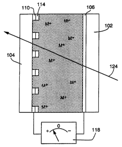
Figure 1 is a cross sectional view depicting the general design of an
electrochemical device constructed according to our invention (some
dimensions,
particularly layer thicknesses, are disproportionate in the drawings in order
to more
2o effectively illustrate the structure and function of the invention). The
device, which
allows precise, reversible control over the transmission of electromagnetic
radiation,
4
CA 02313398 2000-06-07
WO 99/32929 PGTNS98/26610
includes first and second substrates 102 and 104 which are substantially
transparent to
the radiation to be controlled. An electrically conducting and
electrochemically stable
film 106, which is also substantially transparent, is deposited on the first
substrate.
The film 106 functions as a first electrode. A second electrochemically stable
s electrode 110 is deposited on the second substrate. Unlike the first
electrode 106,
however, the second electrode 110 is applied in a special configuration.
Rather than
being deposited in a uniform layer, the second electrode is distributed in
localized
areas on the second substrate.
An electrolytic solution 112 is located between and in electrical contact with
the electrodes 106 and 110. In the configuration depicted by Figure 1, the
device is
initially charged by depositing a metallic layer 114 on the locally
distributed electrode
110, i.e., the layer 114 is deposited on the electrode 110 prior to assembly
of the
device. As those skilled in the art will appreciate, and as further explained
in the
discussion below regarding the operation of the device, this metallic layer
may be,
~ s alternatively, initially deposited on the electrode 110, on the electrode
106, or divided
between a partial deposit on the electrode 106 and a partial deposit on the
electrode
110. The amount of metal in this initially deposited layer or layers
establishes the
maximum amount of metal which will be available for deposit, as explained in
more
detail below, to control the transmittance of the device. Metal ions 116,
which contain
2o the same metal atoms as the layer 114, are dissolved within the
electrolytic solution
112 such that the metal atoms in solution can be reversibly electrodeposited
on and
electrodissolved from the first and second electrodes.
The device is intended for use in conjunction with a source of electrical
potential 118 which has a reversible polarity and an adjustable potential
value. The
2s source 118 is connected between the first and second electrodes 106 and
110. When a
negative electrical potential is applied to the first electrode 106 relative
to the second
electrode 110, metal 114 deposited on the second electrode 110 will tend to be
dissolved from the second electrode into the electrolytic solution 112, while
metal
CA 02313398 2000-06-07
WO 99/32929 PC'f/US98/26610
ions 116 in the solution will tend to be electrodeposited from the solution
onto the
first electrode 106.
When the polarity of the applied potential is reversed, such that a positive
potential is applied to the first electrode 106 relative to the second
electrode 110,
s deposited metal will tend to be dissolved from the first electrode into the
solution 112
and dissolved metal will tend to be electrodeposited from the solution onto
the second
electrode.
The amount of deposited metal which remains on the first electrode will
determine the impediment which the device presents to the radiation. Since the
second
electrode is distributed in localized areas, metal deposited on the second
electrode will
not substantially impede the transmission of radiation through the device,
much like
the scene outside a window can be easily viewed through a window screen made
of a
grid of wire or fiberglass. The process is reversible and may be maintained at
virtually
any point between substantially complete deposition on and substantially
complete
~ s erasure from the first electrode. Thus the device may be adjusted to any
transmissive
value from approximately 0% to approximately 100%.
Figure 2 is a cross sectional view similar to Figure 1, but illustrating the
performance of the device when su~cient negative electrical potential has been
applied to the first electrode relative to the second electrode for a su~cient
period of
2o time to cause a substantial layer of the metal to deposit onto the first
electrode. In this
condition, a layer 120, created by the deposited metal, will tend to impede
the
transmission of radiation, illustrated by the light beam 122, which impinges
on the
device, either by reflection or by absorption, as explained further below.
Figure 3 is a cross sectional view similar to Figures 1 and 2, but
illustrating the
2s behavior of the device when sufficient positive electrical potential has
been applied to
the first electrode relative to the second electrode for a sufficient period
of time to
cause substantially all of the metal to dissolve from the first electrode and
to deposit
as the distributed metallic layer 114 on the second electrode. In this
condition, the
mirror will impose a minimal impediment to incoming radiation, thereby
allowing
6
CA 02313398 2000-06-07
WO 99/32929 PCT/US98/26610
substantially all such incoming radiation to be transmitted through the
device, as
illustrated by the light beam 124.
Figure 4 is a cross sectional view of a "curtained" version of the device
which
is capable of forming both a reflective minor layer and a black, absorbing
curtain
s layer. In this embodiment, an electrically conducting transparent film 406a
is
deposited on a transparent substrate 402a, while another electrically
conducting
transparent film 406b is deposited on a transparent substrate 402b. Between
these
components, a substrate 404 has a locally distributed electrode 410a deposited
on one
side, with a similar locally distributed electrode 410b deposited on the other
side. As
explained above in connection with the embodiment depicted in Figures 1-3, the
device is initially charged with metallic layers 114a and 114b deposited on
electrodes
410a and 410b, respectively. Electrolyte solution 412a is positioned between
and in
electrical contact with the electrodes 406a and 410a, while an electrolyte
solution
412b is positioned between and in electrical contact with the electrodes 406b
and
15 410b. Metal ions 416a are dissolved within the solution 412a, while metal
ions 416b
are dissolved within the solution 412b. The solutions 412a and 412b may be the
same
or different, but should typically be chosen to optimize the operation of the
respective
sides of the device, as explained in more detail below. Similarly, the ions
416a and
416b may be identical or different, depending on the structural and operating
2o parameters chosen for each side of the device. A surface modification layer
408 on the
electrode 406a facilitates nucleation of electrodeposited metal on the
electrode in a
substantially uniform mirror layer.
A negative electrical potential applied to the electrode 406a, relative to the
electrode 410a, will cause metal ions to deposit in a substantially uniform
layer on the
2s surface modification layer 408, forming a minor surface which will reflect
light
passing through the device from the right side of Figure 4. A negative
electrical
potential applied to the electrode 406b, relative to the electrode 410b, will
cause metal
ions to deposit on the electrode 406b. Because of the design parameters chosen
for
this electrode, including the absence of a surface modification layer on the
electrode
7
CA 02313398 2000-06-07
WO 99/32929 PCTNS98/26610
410b, however, the tatter deposit will tend to be finely divided and porous,
so that it
appears black or gray. This deposit will thus tend to block the transmission
of light
through the device from the left by absorption. This embodiment thus provides
the
user with the option to employ both absorbing and reflecting layers, each of
which
may be adjusted for the amount of absorption or reflection, respectively. One
use for
such a device would be in the sunroof of an automobile. When the device is
configured to form a substantially reflecting mirror surface, the mirror
surface will
tend to reflect both light striking the surface from outside of the vehicle as
well as
from the interior of the vehicle. Since such a reflective panel might be
undesirable on
the interior ceiling of the automobile, the curtain layer can be activated so
that the
sunroof would appear as a darkened non-reflective panel from the interior. The
curtained embodiment may also be used where heating is desired, e.g., by means
of
heat radiated and/or conducted as a result of the light absorbed by the layer.
Fabrication of a Preferred Embodiment
The preferred first electrode utilizes a glass or plastic substrate which is
uniformly coated on one side with a transparent, high conductivity (S 10
S2/square)
ITO (indium tin oxide) film. An electrical bus connection is formed around the
perimeter of the ITO coating with conducting Ag epoxy or a vacuum evaporated
metal
strip.
2o The preferred second electrode includes an adherent, electrochemically
inert
metal grid pattern, e.g., Ti/Au or Cr/Au, deposited on a glass or plastic
substrate via
vacuum deposition. A square, electrically continuous grid pattern with 25 wm
wide
lines 500 p.m apart will provide ~ 90% light transmission. The grid is
electrically
connected through a Ag epoxy or evaporated metal bus around the perimeter of
the
2s substrate. Prior to cell assembly, the grid is plated with a quantity of
metal, an excess
being preferable. (Alternatively, the first electrode can be plated in this
fashion).
The preferred electrolyte is an optically clear gel electrolyte with the
following
components:
8
CA 02313398 2000-06-07
WO 99/32929 PCT/US98/26610
1. An appropriate solvent with a low freezing point, high boiling point, and
high
dielectric constant, e.g., propylene carbonate (~p. -49°C, b.p.
241°C), or y
butyrolactone (fp. -43°C, b.p. 202°C). These solvents have large
windows of
electrochemical potential stability and are used in commercial batteries and
electrolytic capacitors.
2. A supporting electrolyte salt, such as a lithium salt with a strongly
acidic
anion, e.g., perchlorate, hexafluorophosphate, trifluoromethanesulfonate,
bistrifluoromethanesulfonimide, etc., to provide conductivity to the
electrolyte.
Electrolytes of such lithium salts (~ 1 M) in a propylene carbonate (PC) or Y-
butyrolactone (GBL) solvent are highly conductive and are used in advanced
batteries and capacitors. Other soluble supporting electrolyte salts, e.g.,
containing other alkali metal ions or tetraalkylammonium ions, can also be
used.
3. An active metal salt or complex which is soluble (~0.1 - 1 M), and
~ 5 thermally/photolytically stable in the above lithium salt electrolyte, to
enable
the reversible plating of the metal layer onto the first and second
electrodes.
This salt can be based on various metal ions, e.g., silver(I), copper(I),
bismuth(III), or other metal systems. Examples include silver perchlorate and
silver trifluoromethanesulfonate.
20 4. An additive to complex the metal ions, which may be required by some
systems to stabilize them with respect to thermal or photolytic decomposition
to the elemental metals and increase the voltage required for
electrodeposition
(thus improving the plating quality). For example, Ag(I) and Cu{I) can be
stabilized by nitriles, amines, phosphines, sulfur donors, etc., e.g.
25 [Cu(nitrile)4]CF3S03. Additives may also be desirable for preventing
dendrite
growth, which can lead to electrical shorting.
5. An electrochemically inert polymer stiffener, e.g., polymethylmethacrylate
(PMMA) or polyacrylonitrile (PAN), which dissolves in the liquid electrolyte
to form a transparent plastic-like gel at room temperature. With an
appropriate
9
CA 02313398 2000-06-07
WO 99/32929 PCTNS98/26610
amount of stiffener, the resulting gel electrolyte can retain the conductivity
of
the liquid electrolyte, yet be cut and applied as a "solid state" component. A
typical gel electrolyte composition which is free-standing at room temperature
contains about 6% (by weight) lithium salt (~ 0.5 - 1 M), 4% silver salt (---
0.1 -
0.5 M), 20% PMMA, and 70% solvent (e.g., PC + benzonitrile stabilizer).
This composition may be cast onto a glass sheet (at elevated temperature or
with excess volatile solvent), allowed to cool or evaporate to the desired
level,
peeled off of the glass, and then sandwiched between the two electrodes.
The electrochemical device of this invention can be fabricated using a liquid
(without the polymer stiffener) or a gel electrolyte, with the latter being
preferred.
In both cases, the two electrodes may be separated by a gasket or O-ring of
appropriate chemical compatibility (e.g., silicone rubber). The preferred
electrode
separation is about 0.5 - 3.0 mm and contains either the liquid or gelled
electrolyte. Electrical contact is made to the metal/silver epoxy bus on each
~ 5 electrode and connected to a voltage source for switching.
Examples
1. An electrolyte was prepared containing 1.35 g silver perchlorate (~0.2 M),
1.91 g
lithium perchlorate (~0.6 M), and 7.62 g PMMA in 7.5 ml BN and 22.5 ml PC.
The first electrode was a 7.6 cm diameter glass disk with a 10 S?Jsquare ITO
2o coating and a 15 A titanium/40 ~r gold flash. (The titanium underlayer
enhanced
the adhesion of the gold to the ITO). The second electrode was fashioned from
a
glass substrate with a fine evaporated Ti/Au 1,000 A square grid pattern with
25
p,m thick lines separated by 500 p,ln spacings; S coulombs (~ 5.6 mg) of
silver
were electroplated onto the grid. Electrical contacts were made to both
electrodes
2s via peripheral strips of silver epoxy which were located outside of and not
in
contact with the electrolyte. Cell fabrication was carried out by sandwiching
the
electrolyte (which flowed slowly at 100°C) between the electrodes,
using a 2.4
mm thick silicone rubber O-ring spacer/seal. and clamping the assembly
together
CA 02313398 2000-06-07
WO 99/32929 PCT/US981Z6610
in a circular frame; excess electrolyte was rinsed away with acetone. The cell
was
switched at t 0.3 V between transparency and a mirror.
2. An example of a system which forms a mirror deposit using an ITO first
electrode
without a nucleating layer is based on a silver cyanide electrolyte
composition: 15
g/L AgN03, 23.5 g KCN, 15 g K2C03, in 400 ml of water. A mirror deposit forms
on the ITO second electrode when biased at -0.6V versus Ag/Ag(CN) 2. The
silver
erases upon biasing at +0.6V.
3. If a mirror deposit is not required, one could construct a device employing
a
locally distributed electrode and an electrolyte, without a nucleating layer.
Such a
1o device can be designed to yield a finely divided, black or gray deposit.
The
aqueous bismuth electrolyte reported by Howard and Ziegler (Solar Energy
Materials and Solar Cells, Volume 39, Pages 309-316 ( 1995)), for example,
provides such a deposit which will tend to absorb rather than reflect light
propagating through the device.
Features of the Invention
It may be desirable for some applications to use a second electrode vrith an
inert metal pattern which is not electrically continuous. Since the
overvoltage for
metal deposition on conducting oxides like ITO is much greater than on a
metal, inert
2o metal islands distributed on a conducting oxide film, which lowers the
sheet
resistance, will behave like localized isolated electrodes with respect to the
metal
deposition. In this embodiment of the invention, current is conducted through
the
conducting substrate film (e.g., ITO) to the metallic islands without causing
metal
electrodeposition elsewhere. The voltage is chosen so that the metal
electrodeposits
only on the isolated metal sites, although current to the sites is carried by
the
underlying conducting oxide film. A second electrode pattern could thus be
chosen to
be less perceptible to the eye, e.g., a fine dot matrix. Conversely, a pattern
could be
selected to be intentionally visible for aesthetic effects, e.g., an array
patterned to
represent an image.
11
CA 02313398 2000-06-07
WO 99/32929 PCT/US98/26610
The second electrode, which can be in the form of a fine inert metal mesh,
like
a window screen, enables most of the light to be transmitted. Such a fine
grid, which
localizes the metal deposit for maximum light transmission, permits the use of
the
same reversible electrochemical reaction (metal electrodeposition/dissolution)
at both
electrodes, greatly simplifying the overall system, eliminating the need for a
cell
separator, and avoiding high voltages. Thus, the system involves a net
reversible
transfer of the same metal from a plated layer at one electrode to a
distributed
localized state at the other, with no net chemical change in the overall
system. Very
little voltage is required for switching and it is not necessary to maintain
an applied
voltage to preserve a given switched state. This is attained by excluding
redox species
other than the metal ions to be deposited from the electrolyte and by limiting
the
operating voltage so that solventlcounterion breakdown is thermodynamically
not
possible. A fine grid counter electrode localizes the second electrode deposit
for
maximum light transmission.
~ 5 No highly energetic species are produced at the electrodes. As a result, a
particular switched state is maintained indefinitely at open circuit.
The device of this invention requires neither a high electrode surface area
nor
high electrical capacity, so that metal traces (having high electrical
conductivity) can
be used and much greater window transparency can be attained via finer line
widths,
2o greater spacing, or smaller dot diameters.
High light transmission through the second electrode is attained via a fine
electrochemically stable metal mesh pattern (deposited on glass or plastic) to
localize
the metal deposit.
The electrochemical device is operated well within the electrolyte stability
25 region, so that excessive metal plating or deplating is not harmful. In
fact, the device
is self limiting for both electrodes when biased within the voltage stability
region,
since the current will practically cease when the deposited metal is depleted
at either
electrode. By limiting the amount of metal deposited on the second electrode
prior to
12
CA 02313398 2000-06-07
WO 99/32929 PCT/US98I26610
cell assembly, overplating of the first electrode under a protracted applied
voltage is
precluded.
No cell separator is needed since the same redox couple (metal
deposition/dissolution) involving a solid product is used at both electrodes
and side
s reactions are avoided.
A wide temperature operating range is obtained by using electrolytes based on
high boiling organic solvents, e.g., propylene carbonate, sulfolane, y-
butyrolactone,
tetraglyme, etc.). Use of mixtures of these solvents can extend the
temperature range
to lower operating temperatures.
Use of a "solid state" gel electrolyte which incorporates an electrochemically
inert polymer stiffener facilitates device fabrication and minimizes
sensitivity to
atmospheric contamination by preventing convectional transport (diffusion is a
very
slow process) as well as cell leakage.
The preferred embodiments of this invention have been illustrated and
~ s described above. Modifications and additional embodiments, however, will
undoubtedly be apparent to those skilled in the art. Furthermore, equivalent
elements
may be substituted for those illustrated and described herein, parts or
connections
might be reversed or otherwise interchanged, and certain features of the
invention may
be utilized independently of other features. Consequently, the exemplary
2o embodiments should be considered illustrative, rather than inclusive, while
the
appended claims are more indicative of the full scope of the invention.
13