Note: Descriptions are shown in the official language in which they were submitted.
CA 02313630 2000-07-OS
BACKGROUND OF THE INVENTION
1. Field of the Invention
The invention pertains to the field of document scanners. Specifically, the
present
invention relates to scanners for documents having some form of conductive
indicia
l embedded, imprinted or affixed thereon.
2. Description of the Related Art
The sale of lottery tickets is a multi-billion dollar a year business. These
tickets are
nearly universally available in grocery stores, convenience stores and
countless other venues.
They provide inexpensive and safe opportunities for consumers to spend a small
amount of
money in exchange for a chance to win goods, services or cash. Moreover, the
sale of lottery
tickets often benefits the local community by providing a welcome additional
source of
funding for education and health programs, among others.
One popular type of lottery tickets is the so-called scratchable lottery
ticket, in which
a number of discrete areas of the ticket are covered with a latex or similar
material that
covers underlying symbols, numbers or icon-like drawings. An example of such a
scratchable lottery ticket is shown at reference numeral 100 in Fig. 1. In
such a typical
lottery ticket, the buyer scratches the latex covering layers 110 from all or
only a few such
areas, to reveal the underlying symbols, numbers or icons. In such tickets,
winning is often
achieved by matching a number of such symbols, by spelling a given word, or by
completing
a sequence. An example of a scratchable lottery ticket in which a plurality of
latex areas has
been scratched off is shown at 200 in Fig. 2. For example, by scratching off
five latex
covered areas and matching three of the underlying symbols, numbers or icons,
the buyer
1
CA 02313630 2000-07-OS
wins a free ticket, a prize or a predetermined cash sum. In Fig. 2, two icons
are shown
within the areas identified by reference numerals 220 and 230. In this manner,
by scratching
off the latex covering from five areas and matching the dollar bill icons
shown in areas 220
three times, the buyer may redeem his or her lottery ticket for a
predetermined cash payment.
A great many such tickets are sold annually. To determine whether a given
lottery
ticket is a winning ticket, therefore, requires countless hours from the
cashiers, store
employees and the like who must closely examine the ticket and make the
appropriate
decisions. It is thus desirable to automate this process. Moreover, lottery
ticket fraud is
sometimes difficult to detect. For example, some latex covered areas may have
been
partially scratched off and re-covered, without the knowledge of the store
owner or the
person that is charged with making the determination as to whether a
particular ticket is a
winning lottery ticket.
A variety of security measures and systems for automating the reading of such
tickets
have been adopted. For example, conductive ink patterns have recently been
added to the
latex-covered areas. The conductive ink patterns can assume various shapes or
follow
elaborate fine patterns similar to those found in high-density printed
circuits. Such ink
patterns, by their conductive nature, allow the presence, integrity and
uniformity of the latex
layer to be determined using electro-mechanical sensing means. Capacitive
sensors have
been utilized for that purpose. For example, a scratchable lottery ticket may
be inserted in an
appropriate sensing device. As the ticket travels past a number of
transmitting and receiving
electrodes separated by a shielding electrode, the coupling capacitances
between transmitting
and receiving electrodes will be different depending on whether the latex
layer has been
scratched off or not. This is because electric charges accumulate on the
conductive ink
patterns applied to the latex as the ticket passes under the electrodes. When
such conductive
2
CA 02313630 2000-07-OS
ink patterns are no longer present or have been fraudulently altered, or when
their
corresponding latex layers have been partially or completely scratched off,
the coupling
capacitances between transmitting and receiving electrodes will differ from a
baseline
capacitance established when the latex layer and conductive ink patterns are
intact.
By correlating the sensed capacitances with their spatial position on the
lottery ticket,
it is possible to determine which of the latex layers have been altered or
scratched off, by
analysis of their electrical signatures. However, this capacitive sensing
method suffers from
a number of drawbacks that limit its effectiveness and functionality. Chief
among these is
the sensitivity of such a capacitive sensor to distance variations between the
conductive ink
pattern and the sensing electrodes. As such lottery tickets have often been
extensively and
rather indelicately handled by the consumer, they may have become deformed or
bent. As
the lottery tickets are introduced into the capacitive sensor device, bends,
creases and other
non-uniform features may adversely affect the capacitive coupling between the
transmitting
and receiving electrodes, and thus the reliability of the reading. Other
sources of distance
variations are misalignment of the sensors within the sensor device itself.
Such a
misalignment may also cause erroneous readings.
The precise distance requirement between the conductive ink pattern and the
sensing
electrodes also implies that a predetermined amount of pressure must be
applied between the
capacitive sensor and the paper media to insure uniformity of the readings.
This makes it
difficult to integrate such capacitive scanning techniques in tandem with
other scanning
techniques, such as optical image sensing. This pressure also makes it
difficult to advance
the ticket through the sensor at high speeds without damage thereto.
Moreover, capacitive coupling sensitivity to distance and misalignment
requires large
electrode plates and therefore inherently limits this technique's ability to
resolve small
3
CA 02313630 2000-07-OS
patterns. What is needed, therefore, is a method and apparatus to electro-
mechanically read
such scratchable lottery tickets that is less sensitive to distance variations
occasioned by
bends and creases in the lottery tickets, as well as by misalignment of the
sensors.
What is also needed is a method and an apparatus to more reliably and
accurately
read such scratchable lottery tickets by sensing and analyzing the electrical
signatures of the
conductive ink patterns applied to the latex covered areas of the tickets.
Furthermore, what are also needed are a method and an apparatus capable of
being
readily scaled down to resolve ever finer and increasingly dense conductive
ink patterns, to
deter fraud.
What is also needed is a non-contact sensing method that is readily applicable
to
high-speed scanners.
SUMMARY OF THE INVENTION
In accordance with the above-described objects and those that will be
mentioned and
will become apparent below, a sensor for determining a state of conductive ink
patterns
applied to scratchable latex layers or similar scratchable layers of instant-
win tickets,
according to an embodiment of the present invention, comprises:
an RF source;
an array of RF transmission antennas, each of the antennas being connectable
in turn
to the RF source to transmit an RF signal across the conductive ink patterns
of the ticket;
at least one RF receiving antenna disposed so as to receive the RF signal
transmitted
across the conductive ink patterns;
signal conditioning means for conditioning received RF signals induced on said
at
least one RF receiving antenna; and
4
CA 02313630 2000-07-OS
computing means for receiving and processing the conditioned signals to
determine
the state of the conductive ink patterns.
According to other embodiments, the sensor may further comprise a switching
circuit
connected between the RF source and the array of RF transmission antennas, the
switching
circuit connecting selected RF transmission antennas of the array to the RF
source according
to a control and timing signal. The array of RF transmission antennas may
comprise, for
example, conductive traces printed on a substrate or coils embedded into the
substrate. The
substrate may be, for example, a printed circuit board, a ceramic material, or
other composite
or machined material suitable for RF applications.
The signal conditioning means may include means for amplifying and isolating
the
signal induced on said at least one RF receiving antenna. The amplifying and
isolating
means may include low noise amplifier means connected to the RF receiving
antenna or
antennas and a discriminator means for substantially eliminating all unwanted
signals outside
of the frequency band of interest. The discriminator means may include
bandpass filter
means, adaptative bandpass filter means, an array of bandpass filter means to
provide a
frequency spectrum measurement, means for measuring the phase change between
the RF
source and the signal induced in the RF receiving antenna or antennas, or
adaptative
bandpass filter means that track the source RF frequency sweep to provide
continuous
spectrum amplitude and phase measurement. The signal conditioning means may
include
means for quantizing signals induced on the RF receiving antenna or antennas,
the quantizing
means being connected to the computing means. The quantizing means may include
sample
and hold (S/H) means and analog to digital converter means. The RF receiving
antenna or
antennas may face the array of RF transmission antennas and may be disposed so
as to allow
the instant-win ticket to be slid between the RF receiving antenna or antennas
and the array
5
CA 02313630 2000-07-OS
of RF transmission antennas. The array of RF transmission antennas and the RF
receiving
antenna or antennas may be disposed so as not to contact the ticket as the
ticket is advanced
through the sensor. The sensor may further comprise a transparent plate
between the array of
RF transmission antennas and the RF receiving antenna or antennas, the ticket
being slid
across the transparent plate by a feed roller during operation of the sensor.
Another embodiment of the present invention is a non-contact method of sensing
a
state of conductive indicia applied to documents, comprising the steps of
generating and transmitting an RF signal in a vicinity and across the
document;
receiving the RF signal, the RF signal being affected by a state of the
conductive
indicia;
conditioning the received RF signal; and
processing the conditioned RF signal so as to extract information relative to
the state
of the conductive indicia.
According to further embodiments of the non-contact sensing method of the
present
invention, the transmitting step may comprise the step of selectively
connecting an RF
source to at least one of a plurality of RF transmitting antennas. The
connecting step may
comprise the step of generating a timing and control signal and transmitting
the timing and
control signal to a switching means to selectively connect the RF source to
one or more of
the plurality of RF transmitting antennas. The receiving step may comprise the
step of
selectively receiving the transmitted RF signal with at least one RF signal
receiving means.
The conditioning step may comprise one or more of the following steps:
amplifying the
received RF signal; discriminating the received RF signal from other signals
received during
the receiving step; and quantizing the received RF signal. The quantizing step
may comprise
6
CA 02313630 2000-07-OS
the steps of sampling and holding the received RF signal; and converting the
sampled and
held signal to digital form suitable for input and processing in digital
processing means. The
discriminating step may comprise one or more of the following steps: bandpass
filtering the
received RF signal; measuring a phase change between the transmitted and
received RF
signals; and adaptatively bandpass filtering the received RF signal while
tracking a
transmitted RF frequency sweep, thereby providing continuous spectrum
amplitude and
phase measurement. A further step of advancing the document past the plurality
of RF
signal transmitting antennas may be carried out during the transmitting and
receiving steps.
BRIEF DESCRIPTION OF THE DRAWINGS
For a further understanding of the objects and advantages of the present
invention,
reference should be made to the following detailed description, taken in
conjunction with the
accompanying figures:
FIG. 1 shows an example of a lottery ticket in which the purchaser is invited
to
scratch off one or more latex covered areas to reveal an icon, image or dollar
amount.
Fig. 2 shows the lottery ticket of Fig. l, with a plurality of latex covered
areas
scratched off by the purchaser, to reveal the images thereunder.
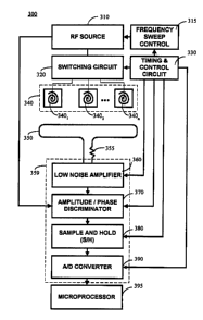
Fig. 3 shows a block diagram of the sensing mechanism of the document scanner
according to an embodiment of the present invention.
Fig. 4 shows one possible physical layout of the major elements of the
inductive
document scanner according to an embodiment of the present invention.
DETAILED DESCRIPTION OF THE INVENTION
The present invention is a method and an apparatus for testing the uniformity
and
integrity of conductive indicia printed, imbedded or otherwise affixed to
documents. One
7
CA 02313630 2000-07-OS
possible application among many such applications relates to determining the
integrity of
latex or other materials covering documents, instant win tickets and the like,
onto which have
been printed a conductive pattern using, for example, conductive ink. The
method and
device according to the present invention sense the integrity of such
conductive ink patterns
and automatically map the scratched off areas of such a lottery ticket.
According to the
present invention, a radio frequency field is created by an array of
transmitting antennas
mounted above and out of contact with or gently applied against the ticket or
other
document, and at least one receiving antenna is placed nearby. When each of
the
transmitting antennas are energized by a radio frequency (hereafter, RF)
source, a signal is
induced and flows through the receiving antenna or antennas as the ticket is
advanced across
and/or over the receiving antenna. The signal induced within the receiving
antenna is
affected by the presence, absence or state of the conductive indicia on the
ticket or document.
By conditioning the received signal and comparing the voltages developed at
the receiving
antenna with pre-determined and pre-stored thresholds while the document is
being advanced
over the array of transmitting antennas, an array of clusters of voltage
magnitudes developed
at the receiving antenna may be constructed. This array of clusters of voltage
values may be
considered a three dimensional map of the conductive ink patterns, as the
array contains both
2-D spatial information as well as voltage magnitudes related to the integrity
of the
conductive ink patterns. Each cluster of voltage values within the array may
be correlated
with individual conductive ink patterns of individual latex covered areas on
the ticket, as the
number and configuration of conductive ink patterns on a given type of ticket
are known, as
is the speed and orientation at which the ticket is fed into the inductive
scanner. The
magnitude of the voltages within each cluster may then be quantized, and the
resultant
numerical values compared, using a table look up scheme, to pre-stored
baseline values.
8
CA 02313630 2000-07-OS
Analyses other than table look up may be carried out; the present invention
not being limited
thereto for analysis of the voltage magnitudes. The result of the comparison
or other analysis
may be utilized to identify fraudulent, tampered, invalid or winning tickets,
or verify the
uniformity of the latex covered areas prior to shipping the lottery tickets or
other document.
An embodiment of the present invention will be described with reference to
Figs. 3
and 4. The inductive document scanner 300 of Fig. 3 includes an RF source 310
having a
predetermined fixed frequency or a variable frequency controlled by the sweep
generator
315. The RF source 310 is connected to the array 340 of transmitting antennas
340,, 3402...
340" via a switching circuit 320. The switching circuit 320 may sequentially
connect each of
the transmitting antennas 340,, 3402... 340 in tum to the RF source 310 while
delivering a
predetermined power level. Alternatively, selected ones of the transmitting
antennas 340,,
3402... 340" may be connected to the RF source 310 in a predetermined
sequence. The
frequency of the switching by the switching circuit 320 must be commensurate
with the
number of transmitting antennas 340,, 3402... 340 within the array 340, the
speed at which
the lottery ticket or other document is advanced across the array 340, as well
as with rise
time of the pulses induced on the receiving antenna 350. For example, the
switching circuit
320 may switch between the transmitting antennas 340,, 3402... 340" every 0.1
ms when
there are ten such transmitting antennas. A timing and control circuit 330
provides the
timing and control signals for the switching circuit 320. Specifically, the
timing and control
circuit 330 provides the switching circuit 320 with an appropriate timing
signal to switch
between the transmitting antennas 340,, 3402... 340n. The sweep generator 315
provides a
sweep control signal to the RF source 310. The sweep generator 315 receives
timing signals
from the timing and control circuit 330.
9
CA 02313630 2000-07-OS
The transmitting antennas 340,, 3402... 340 of the array 340 may be antennas
formed
of a printed conductive material, such as a copper layer on or within a small
printed circuit
board or may be a conductive material deposited on a ceramic substrate, for
example. The
transmitting antennas 340,, 3402... 340" may have a circular spiral shape, a
rectangular spiral
shape or most any other shape that is effective in transmitting at least some
of the radiated
energy toward the conductive ink patterns applied on the lottery ticket or
other document to
be scanned at the selected frequency. Disposed nearby or across from the
ticket or other
document and facing the array 340 of transmitting antennas 340,, 3402... 340"
is at least one
receiving antenna 350. The receiving antenna 350 can be a single elongated
conductive loop
covering substantially the full width of the document, as shown in Fig. 3, an
array of
interconnected elongated conductive loops of predetermined length, or an array
of miniature
RF receiving antennas. In the latter case, a plurality of miniature RF
receiving antennas may
be disposed facing corresponding transmitting antennas 340,, 3402... 340. The
outputs of
each of the plurality of miniature RF receiving antennas may be connected to
the next stage
via a multiplexes controlled by the timing and control circuit 330. The
receiving antenna 350
may be a loop pattern such as a copper layer on a printed circuit board or may
be made by
more elaborate techniques that are known to those of skill in the RF arts.
As the ticket is advanced over the array 340 and as the switching circuit 330
applies
RF energy in turn to each of the transmitting antennas 340,, 3402... 340", a
signal is induced
in the receiving antenna or antennas 350. The magnitude of the induced signal
is a function
of the magnitude of the applied RF energy, the degree of inductive coupling
between the
receiving antenna or antennas 350 and the transmitting antennas 340,, 3402...
340n connected
to the RF source 310, as well as a function of the presence, absence or state
of the conductive
indicia or ink patterns on, within or under the latex covered areas of the
ticket or other
CA 02313630 2000-07-OS
document. Signal conditioning means 359 are connected to the receiving antenna
350. The
signal conditioning means 359 may include a low noise amplifier circuit 360
connected to
the receiving antenna or antennas 350 that amplifies the signal induced on the
receiving
antenna or antennas 350. The timing and control circuit 330 may turn the low
noise
amplifier on and off with the same frequency as it applies RF power to the
transmitting
antennas 340" 3402... 340", thus ensuring that the signal amplified is indeed
the signal of
interest, i.e. a signal that corresponds in time to one of the conductive
patterns on the latex
covered areas as the ticket is advanced through the sensor. Alternatively, the
low noise
amplifier 360 may operate continuously, independently of the timing and
control circuit 330.
An amplitude/phase discriminator circuit 370 is connected to the low noise
amplifier 360.
The discriminator circuit 370 isolates the signal of interest. This may be
carried out, for
example, by a high order bandpass filter, centered on the frequency of the RF
source 310. A
high order filter will insure that only the signal of interest is selected,
greatly attenuating or
eliminating all signals that fall outside the passband of the filter. The
discriminator 370 may
be manually or automatically tunable, to center on a given frequency or to
track the
frequency sweep controlled by the frequency sweep control 315. The
discriminator 370 may
thus comprise an adaptive filter that limits the spectral content of the
amplified signal output
from the low noise amplifier 360 to the frequency band of interest, such as
the frequency of
the RF source 310 or some multiple thereof. This reduces the effects of noise,
and other
unwanted perturbations caused by, for example, other RF signals generated by
motors and
other sources within and/or near the scanner. Moreover, the discriminator may
comprise an
array of filters, each filter of the array being centered around a
predetermined frequency to
provide multiple outputs, thus providing a spectrum analysis measurement. In
an alternative
embodiment, the discriminator may comprise a phase discriminator to measure
the phase
11
CA 02313630 2000-07-OS
change between the RF source and the induced signal. The output or outputs of
the
discriminator 370 may then be input to a sample and hold (S/H) circuit 380.
The S/H circuit
380 may be controlled by a S/H timing signal output from the timing and
control circuit 330,
to insure that the sampling is carried out when the signal of interest is
available at the output
S of the discriminator 370. The sampled and held signal is then converted to
digital form, in
the AID converter 390. An 8 or 12 bit A/D converter may provide sufficient
resolution.
However, A/D converters of higher resolution may also be employed. The timing
of the
conversion is controlled by an AID timing signal output from the timing and
control circuit
330, to insure that the voltages across the storage circuits within the S/H
circuit 380 have
ramped up to their final value. The digitally converted information is then in
a format that is
appropriate for input to a microprocessor or DSP - digital signal processor,
such as
microprocessor 395 in Fig. 3. For example, the digitized information may be
placed on the
microprocessor's data bus by a suitable bus interface, the structure of which
is known to
those of skill in the digital arts. The microprocessor or other processing
engine 395 stores
these digitized values and uses these values to construct and store an array
of clusters of
voltage magnitude values corresponding to the induced signal on the receiving
antenna 350.
Each of the clusters spatially corresponds to a conductive ink pattern or
patterns of an
individual latex covered area on the ticket or other document, such as the
latex covered areas
210, 220 or 230 in Fig. 2. The numerical voltage values within each of the
clusters
correspond to the magnitude of the signal within the spectral band of interest
received at the
receiving antenna or antennas 350
By advancing the lottery ticket (or other document having conductive indicia
thereon)
through the inductive scanner according to the present invention in the
direction indicated by
the arrow 240 in Fig. 2, and by scanning the conductive indicia of the latex
areas in a
12
CA 02313630 2000-07-OS
direction perpendicular thereto, an accurate map or numerical representation
of the
magnitudes of the induced voltages may be constructed. This scanning is
accomplished by
the switching circuit 320 switching between the transmitting antennas 340,,
3402... 340" in
succession or in some predetermined order. For example, each or a selected
transmitting
antenna 340,, 3402... 340" may be energized once or a pre-determined number of
times from
the RF source 310 for every 1 mm, for example, of travel by the lottery ticket
past the
inductive sensor according to the present invention. Therefore, should the
latex covered
areas having the conductive indicia thereon have a width dimension (the
dimension that is
parallel to the direction 240) 1 cm wide, 10 measurements of the induced
voltages will be
taken for each latex covered area. These 10 measurements will be conditioned,
digitized,
stored and analyzed by processing engine 395 within the inductive scanner 300
in the manner
described above. Therefore, with 10 measurements along the width of each of
the latex
covered areas, an accurate digital representation of the conductive ink
patterns on each of the
latex covered areas may be acquired. For greater accuracy, a greater number of
samples may
1 S be acquired per unit length of lottery ticket. However, a point of
diminishing returns may be
reached, where the sampling frequency exceeds that necessary to develop an
accurate
representation of the smallest features of the conductive ink patterns.
Therefore, the
sampling frequency and thus the frequency of the switching circuit 320 density
will be
adjusted according to the requirements of the application at hand, with the
finest feature of
the conductive indicia dictating the choice of frequency in the RF source 310.
Fig. 4 shows the cross-section of one possible physical layout of the major
elements
of the inductive document scanner according to an embodiment of the present
invention.
The document to be scanned with the conductive indicia printed or affixed
thereon is shown
at reference numeral 420. Such a document 420 may be, for example, a lottery
ticket, such
13
CA 02313630 2000-07-OS
as shown at 200 in Fig. 2. The direction along which the document 420 is
introduced into the
inductive scanner according to the present invention is shown at 425.
According to one
embodiment, the operator manually advances the document 420 into the scanner
along the
direction 425 until the document is grabbed by the rotating feed roller 410.
S Advantageously, the inductive scanner according to the present invention may
be
equipped with the Anti-Skew Auto-Start features and structures disclosed in
commonly
assigned US patent application Serial Number 08/904,337, the disclosure of
which is
incorporated herewith by reference. In this manner, the feed roller 410 will
only grab the
document 420 when it is acceptably aligned, thus ensuring accurate and
trustworthy
measurements of the state of the conductive ink patterns printed on or
embedded in the latex
covered areas of the document 420.
As the feed roller 410 rotates in the direction of the arrow 415, the document
420 is
grabbed and slid across the transparent plate 460 and over the optical sensor
430. The
optical sensor 430 may be used for a variety of tasks, such as optical
character recognition,
or detection of any number of visible security features on the document 420.
The optical
sensor 430 may include a plurality of proximity sensors to detect the size and
orientation of
the document inserted into the inductive sensor according to the present
invention. A simple
vote algorithm of the sensors that are activated by the presence of the
document 420 enables
the determination of document size and position. A scanner controller module,
such as
disclosed in commonly assigned US patent application No. 08/931,131, the
disclosure of
which is hereby incorporated by reference, may be advantageously utilized to
provide the
necessary control signals for the sensor.
According to one embodiment of the present invention, the transmitting antenna
array
440 and the receiving antenna or antenna array 450 (similar to elements 340
and 350 in Fig.
14
CA 02313630 2000-07-OS
3, respectively) may face each other on either side of the document 420 as it
is advanced by
the feed roller, as shown in Fig. 4. In this manner, the lines of magnetic
flux developed by
the array 440 cut through the document 420 and the conductive ink patterns
disposed
thereon. The induced current on the receiving antenna or antennas 450 will,
therefore, be
partially modulated depending on the presence, absence or partial presence of
the conductive
ink patterns on the document 420. By conditioning, digitizing, storing and
analyzing the
waveforms induced on the receiving antenna or antennas 450, the state (intact,
partially
scratched off or missing, for example) of the conductive indicia (and hence of
the latex layer)
may be determined by suitable signal processing in the microprocessor 395. The
RF
transmission antennas 340,, 3402... 340 and the RF receiving antenna or
antennas 350 are
preferably disposed a distance away from the ticket as it is advanced through
the sensor.
This non-contact method does not damage the latex layer when the ticket is
advanced at high
speed through the sensor and is suitable for integration into high-speed
optical scanners.
While the foregoing detailed description has described several embodiments of
this
invention, it is to be understood that the above description is illustrative
only and not limiting
of the disclosed invention. For example, the shape, number, configuration and
location of
the transmitting and receiving antennas may differ from the embodiments
described herein.
Moreover, the signal conditioning elements disclosed herein may vary from that
described
and illustrated without, however, departing from the spirit and scope of the
present invention.
A number of other modifications will no doubt occur to persons of skill in
this art. All such
modifications, however, should be deemed to fall within the scope of the
present invention.
Thus, the invention is to be limited only by the claims as set forth below.