Note: Descriptions are shown in the official language in which they were submitted.
CA 02313656 2000-07-10
Patent Application
Attorney Docket No. D/991571
FLANGE DEVICE WITH FINISHED SURFACE
This invention relates in general to a conductive composite
flange device for supporting a hollow cylindrical member without the use of an
adhesive or additional grounding member.
The xerographic imaging process begins by charging a
photoconductive member to a uniform potential, and then exposing a light
image of an original document onto the surface of the photoreceptor, either
directly or via a digital image driven laser. Exposing the charged
photoreceptor to light selectively discharges areas of the surface while
allowing other areas to remain unchanged, thereby creating an electrostatic
latent image of the document on the surface of the photoconductive member.
A developer material is then brought into contact with the surface of the
photoreceptor to transform the latent image into a visible reproduction. The
developer typically includes toner particles with an electrical polarity
opposite
that of the photoconductive member. A blank copy sheet is brought into
contact with the photoreceptor and the toner particles are transferred thereto
by electrostatic charging the sheet. The sheet is subsequently heated,
thereby permanently affixing the reproduced image to the sheet. This results
in a "hard copy" reproduction of the document or image. The photoconductive
member is then cleaned to remove any charge and/or residual developing
material from its surface to prepare it for subsequent imaging cycles.
Electrostatographic imaging members are well known in the art.
One type of photoreceptor conventionally utilized for copiers and printers
comprises a hollow electrically conductive drum substrate which has been dip
coated with various coatings including at least one photoconductive coating
1
CA 02313656 2000-07-10
comprising pigment particles dispersed in a film-forming binder. These
photoreceptors are usually supported on an electrically conductive shaft by
drum supporting hubs or end flanges. The hubs are usually constructed of
plastic material and have a hole through their center into which a supporting
axle shaft is inserted. Since hubs are usually constructed of electrically
insulating plastic material, an electrical grounding means comprising a
flexible
spring metal strip is secured to the hub and positioned to contact both the
electrically conductive axle shaft and the electrically conductive metal
substrate of the photoreceptor drum.
Unfortunately, this metal ground shim is often bent out of
alignment when inserted into one end of a photoreceptor drum. Such
misalignment can result in the metal strip not contacting the interior of the
drum or the axle or both after insertion of the hub into the end of the drum
is
completed. Further, coatings electrically insulating in the dark that are
formed
on the surface of the interior of the drum during dip coating can adversely
affect electrical grounding of the drum to the electrically conductive drum
axle
shaft. If inadequate electrical grounding of the drum to the axle shaft is
detected after the drum has been inserted into a modular replacement unit in
which photoreceptor and various other subsystems such as cleaning and
charging units are permanently mounted, repair of the drum is usually
impossible without destruction of the module.
Accordingly, a need remains for an apparatus which is capable
of supporting hollow cylindrical members without the use of an adhesive, to
facilitate recycling.
In one aspect of the invention, a flange device is arranged for
forming a conductive interference fit with a photoreceptor, the photoreceptor
comprising a hollow cylindrical member having an inner diameter, an inner
surface and enclosing a cavity, the flange device comprising a flange, the
flange comprising a conductive plastic and having a length, a diameter and a
2
CA 02313656 2000-07-10
surface, the flange length and diameter being sized so that, when the flange
is
inserted in the photoreceptor cavity, an interference fit is formed between
the
flange surface and the photoreceptor inner surface; the flange surface being
finished so that sufficient friction exists between the flange surface and the
photoreceptor inner surface to enable the flange to rotatably drive the
photoreceptor.
In another aspect of the invention, a method of forming a ground
circuit between a photoreceptor and an electrostatographic machine, the
photoreceptor comprising a hollow cylindrical member having an inner
diameter, an inner surface and enclosing a cavity, comprises the steps of:
forming a flange device made of conductive plastic, the flange device
including
a flange support member and a flange; sizing the flange with respect to the
photoreceptor inner diameter; fitting the flange in the photoreceptor cavity,
where the flange is sized and shaped with respect to the inner diameter so as
to provide an interference fit to withstand compressional and torsional forces
applied to the flange device; and contacting a conductive photoreceptor
support to the flange device, thereby completing the electrical ground circuit
between the photoreceptor, flange device and electrostatographic machine;
where the forming step includes a step of finishing the flange surface so that
sufficient friction is established between the flange surface and the inner
diameter of the photoreceptor.
In still another aspect of the invention, a flange device and a
photoreceptor are combined, the photoreceptor comprising a hollow cylindrical
member having an inner diameter, an inner surface and enclosing a cavity, the
flange device comprising a flange, the flange comprising a conductive plastic
and having a length, a diameter and a surface, the flange extending in the
photoreceptor cavity, the flange length and diameter being sized so that a
conductive interference fit is formed between the flange surface and the
photoreceptor inner surface; the flange surface being finished so that
sufficient
3
CA 02313656 2003-05-29
friction exists between the photoreceptor inner surface and the flange surface
to
enable the photoreceptor to be rotatably driven by the flange.
In another aspect of the present invention, there is provided a
flange device capable of translating a rotational force from an outside source
to a
hollow cylindrical member having an inner surface comprising: a flange support
member for applying the rotational force; and a flange connected to the flange
support member, the flange being made from a conductive plastic and having a
length, an inner diameter, and an outer diameter, wherein the outer diameter
of
the flange is sized with respect to the inner surface of the hollow
cylindrical
member and the length of the flange is such that an interference fit is formed
between the flange and the inner surface of the hollow cylindrical member, the
interference fit being maintained in the absence of an adhesive and thereby
forming an electrical path between the flange and the hollow cylindrical
member.
In another aspect of the present invention, there is provided a
method of forming a ground circuit between a photoreceptor having an inner
diameter and an electrostatographic machine, comprising: forming a flange
device made of conductive plastic, the flange device including a flange
support
member and a flange; sizing the flange with respect to the inner diameter of
the
photoreceptor; fitting the flange in the photoreceptor, wherein the flange is
sized
and shaped with respect to the inner diameter of the photoreceptor so as to
provide an interference fit to withstand compressional and torsional forces
applied to the flange device; and contacting a conductive photoreceptor
support
to the flange device thereby completing the electrical ground circuit between
the
photoreceptor, flange device and electrostatographic machine.
In another aspect of the present invention, there is provided a
method of forming a ground circuit between a photoreceptor having an inner
diameter and an electrostatographic machine, comprising: forming a flange
device made of conductive plastic the conductive plastic including
approximately
82 wt. % polycarbonate, 12 wt. % carbon and 6 wt. % TefIonTM, the flange
device
4
CA 02313656 2004-02-16
including a flange support member and a flange; sizing the flange with respect
to the inner diameter of the photoreceptor, fitting the flange in the
photoreceptor, wherein the flange is sized and shaped with respect to the
inner diameter of the photoreceptor so as to provide an interference fit to
withstand compressional and torsional forces applied to the flange device;
and contacting a conductive photoreceptor support to the flange device,
thereby completing the electrical ground circuit between the photoreceptor,
flange device and electrostatographic machine.
According to an aspect of the present invention, there is
provided a flange device arranged for forming a conductive interference fit
with a photoreceptor, the photoreceptor comprising a hollow cylindrical
member having an inner diameter, an inner surface and enclosing a cavity,
the flange device comprising a flange, the flange comprising a
conductive plastic and having a length, a diameter and a surface, the
conductive plastic comprising a polymer plastic, a non-stick material, and one
of carbon fiber and metal flakes,
the flange length and diameter being sized so that, when the
flange is inserted in the photoreceptor cavity, an interference fit is formed
between the flange surface and the photoreceptor inner surface;
the flange surface being finished so that sufficient friction exists
between the flange surface and the photoreceptor inner surface to enable the
flange to rotatably drive the photoreceptor.
According to another aspect of the present invention, there is
provided a method of forming a ground circuit between a photoreceptor and
an electrostatographic machine, the photoreceptor comprising a hollow
cylindrical member having an inner diameter, an inner surface and enclosing
a cavity, the method comprising the steps of:
forming a flange device made of conductive plastic, the flange
device including a flange support member and a flange, the conductive plastic
comprising a polymer plastic, a non-stick material, and one of carbon fiber
and metal flakes;
4a
CA 02313656 2004-02-16
sizing the flange with respect to the photoreceptor inner
diameter;
fitting the flange in the photoreceptor cavity, where the flange is
sized and shaped with respect to the inner diameter so as to provide an
interference fit to withstand compressional and torsional forces applied to
the
flange device; and
contacting a conductive photoreceptor support to the flange
device, thereby completing the electrical ground circuit between the
photoreceptor, flange device and electrostatographic machine;
where the forming step includes a step of finishing the flange
surface so that sufficient friction is established between the flange surface
and
the inner diameter of the photoreceptor.
According to a further aspect of the present invention, there is
provided in combination:
a flange device and a photoreceptor,
the photoreceptor comprising a hollow cylindrical member
having an inner diameter, an inner surface and enclosing a cavity,
the flange device comprising a flange, the flange comprising a
conductive plastic and having a length, a diameter and a surface, the
conductive plastic comprising a polymer plastic, a non-stick material, and one
of carbon fiber and metal flakes,
the flange extending in the photoreceptor cavity, the flange
length and diameter being sized so that a conductive interference fit is
formed
between the flange surface and the photoreceptor inner surface;
the flange surface being finished so that sufficient friction exists
between the photoreceptor inner surface and the flange surface to enable the
photoreceptor to be rotatably driven by the flange.
According to another aspect of the present invention, there is
provided a flange device capable of translating a rotational force from an
outside source to a hollow cylindrical member having an inner surface
comprising:
a flange support member for applying the rotational force; and
4b
CA 02313656 2004-02-16
a flange connected to the flange support member, the flange
being made from a conductive plastic and having a length, an inner diameter,
and an outer diameter, wherein the conductive plastic comprises a polymer
plastic, a non-stick material, and one of carbon fiber and metal flakes; the
outer diameter of the flange is sized with respect to the inner surface of the
hollow cylindrical member and the length of the flange is such that an
interference fit is formed between the flange and the inner surface of the
hollow cylindrical member, the interference fit being maintained in the
absence of an adhesive and thereby forming an electrical path between the
flange and the hollow cylindrical member.
According to a further aspect of the present invention, there is
provided a method of forming a ground circuit between a photoreceptor
having an inner diameter and an electrostatographic machine, comprising:
forming a flange device made of conductive plastic, the flange
device including a flange support member and a flange, the conductive plastic
comprising a polymer plastic, a non-stick material, and one of carbon fiber
and metal flakes;
sizing the flange with respect to the inner diameter of the
photoreceptor;
fitting the flange in the photoreceptor, wherein the flange is sized
and shaped with respect to the inner diameter of the photoreceptor so as to
provide an interference fit to withstand compressional and torsional forces
applied to the flange device; and
contacting a conductive photoreceptor support to the flange
device, thereby completing the electrical ground circuit between the
photoreceptor, flange device and electrostatographic machine.
According to another aspect of the present invention, there is
provided a method of forming a ground circuit between a photoreceptor
having an inner diameter and an electrostatographic machine, comprising:
forming a flange device made of conductive plastic, the
conductive plastic comprising approximately 82 wt.% polycarbonate, 12 wt.%
4c
CA 02313656 2004-02-16
carbon fiber and 6 wt.% PolyTetraFluoroEthylene (PTFE), the flange device
including a flange support member and a flange;
sizing the flange with respect to the inner diameter of the
photoreceptor;
fitting the flange in the photoreceptor, wherein the flange is sized
and shaped with respect to the inner diameter of the photoreceptor so as to
provide an interference fit to withstand compressional and torsional forces
applied to the flange device; and
contacting a conductive photoreceptor support to the flange
device, thereby completing the electrical ground circuit between the
photoreceptor, flange device and electrostatographic machine.
In one embodiment, the conductive plastic includes
approximately 82 wt. % polycarbonate, 12 wt. % carbon fiber and 6 wt.
TeflonTM.
FIG. 1 depicts a three dimensional view of a conductive flange
device 102 of the present invention as mounted to an electrostatographic
photoreceptor 10.
FIG. 2 is a front view of the flange of the present invention.
FIG. 3 is a rear view of the conductive composition flange of the
present invention.
FIG. 4 is a side view of the conductive composite flange device
102 of the present invention, the flange device 102 including an outer
diameter 106 and a corresponding outer diameter surface 106A.
FIG. 5 is a front view of the flange device 102, including the
foregoing outer diameter 106 and the corresponding outer diameter surface
106A.
FIG. 6 is a schematic view of the assembly device for inserting
the flange device.
While the present invention may be employed in any suitable
device that requires support for a drum, it will be described herein with
reference to and more specifically to a conductive composite end flange for
4d
CA 02313656 2004-02-16
supporting hollow cylindrical support members in an electrostatographic
imaging system without the use of an adhesive.
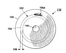
Referring now to the drawings, FIG. 1 depicts a schematic, three
dimensional view of the conductive photoreceptor flange of the present
invention, mounted to an electrostatographic photoreceptor as indicated by
10. Flange 102 is connected to flange support member 104. Flange and
flange support member form flange device 110.
4e
CA 02313656 2000-07-10
As shown, photoreceptor 12 comprises a hollow cylindrical
member with inner diameter 18 and corresponding inner surface 18A, the
photoreceptor 12 enclosing a cavity or hollow 12A. Also, flange 102 has outer
diameter 106 with corresponding outer surface 106A. As explained below, the
magnitude of flange 102's outer diameter 106 and the physical finish of flange
102's outer surface 106A are selectively arranged so that when flange 102 is
inserted substantially inside photoreceptor 12's inner cavity or hollow 12A
sufficiently so that flange 102 is substantially surrounded by photoreceptor
12,
photoreceptor 12's inner surface 18A and flange 102's outer surface 106A are
caused to sufficiently engage and contact each other, thus forming an
interference fit.
Photoreceptor support 22 supports flange device 110.
Photoreceptor support 22 is conductive and completes the electrical ground
circuit between photoreceptor 12 and flange device 110 and the xerographic
system. Of course photoreceptor support 22 need not pass through the entire
length of the photoreceptor, it being well-known to have a shaft on each end
of
a photoreceptor to separately support each flange device. Photoreceptor
support 22 could also take the form of a drive dog, a conductive shoe or a
conductive roller which contact flange support 104 to drive photoreceptor 12,
rather than a gear as shown and discussed below.
In the embodiment shown, flange support member 104 includes
a gear 20 or similar device mounted to an externally-supplied rotational or
torque drive force such as an electric motor (not shown) to cause rotation of
gear 20 about axis x as indicated by arrow y. Gear 20 is attached to one or
both ends 14 and 16 of photoreceptor 12, causing photoreceptor 12 to rotate
past corona device 24 for charging of the photoreceptor to a uniform
electrostatic potential. A light image of an original document is exposed onto
the surface of photoreceptor 12 to form an image on the photoreceptor
s
CA 02313656 2000-07-10
surface. A developer material is then brought into contact with the surface of
the photoreceptor to transform the latent image into a visible reproduction.
FIGS. 2 and 3 depict front and rear views of conductive
photoreceptor flange 102 of the present invention. As shown, flange 102 has
an outer diameter 106, and a thickness 108.
Referring to FIGS. 4 and 5 it is seen that flange 102 has a length
112, to assist in providing torsional and axial support for photoreceptor 12.
As
mentioned above, flange 102's outer diameter surface 106A is purposely
finished in such a manner as to encourage frictional contact and gripping of
photoreceptor 12's inner surface 18A, the foregoing surface finishing being
specially depicted in FIG. 5 by a series of uneven, bumpy or "wiggley" lines
on
an upper portion of outer diameter surface 106A.
As shown, flange support 104 has opening 120 formed
therethrough for insertion of photoreceptor support 22 in the xerographic
machine. As indicated above, photoreceptor 12 rotates about axis x in the y
direction, due to the rotation of gear 20. As shown, photoreceptor support 22
is a shaft, however may be any type of well-known supports and may include a
dog that attaches directly to flange support 104 and transmits the torsional
force. Flange 102 serves to transfer the torsional force applied by the
outside
source from gear 20 to photoreceptor 12. While flange 102 provides axial as
well as torsional support, the primary loads applied to it result from the
torque
from the outside source. Photoreceptor 12 must often operate under torsional
loads of as much as 45 Ibs-in. Thus, flange 102 must be able to withstand
loads of this magnitude in order to successfully transfer the required torque
from an outside source, such as a motor (not shown), to photoreceptor 12.
It will be appreciated that the magnitudes of length 112, the
magnitude of outer diameter 106, and the finish of outer diameter surface
106A must all be considered when flange 102 is being designed. If design
constraints unrelated to rotation of photoreceptor 12 (such as the
configuration
6
CA 02313656 2000-07-10
of the cavity of the machine) place limitations on either or both of these
dimensions, length 112 can be changed as long as the outer diameter 106's
magnitude and the finish of outer diameter surface 106A are altered
accordingly.
For example, a longer photoreceptor 12 with a relatively small
diameter can be supported by flange 102 as long as flange 102's decrease in
outer diameter 106 is accompanied by a proportional increase in length 112,
increase in roughness of outer diameter surface 106A, or both. Similarly, a
relatively shorter photoreceptor 12 can be supported by flange 102 as long as
flange 102's outer diameter 106 magnitude is increased and the roughness of
outer diameter surface 106A is increased along with any required decrease in
length 112.
Prior to assembly, outer diameter 106 is slightly larger than the
inner diameter 18 of photoreceptor 12. Flange 102 must be forced into the
inside of photoreceptor 12 such that outer diameter 106 will come in firm
contact with the inside surface of photoreceptor 12. This requires
photoreceptor 12 to be manufactured such that it will expand slightly in the
outward radial direction as flange 102 is inserted into its inside surface.
This
also requires flange 102 to be strong enough to withstand the inner radial
compression load that will then be exerted upon it, once it has been press fit
into the inside of photoreceptor 12 and maintain the interference fit
throughout
the printer operating temperature range. Preferably, the outer surface of
flange 102 is controlled in order to prevent scratching or gouging of the
inner
surface of photoreceptor 12 and to optimize the friction between the inner
surface of photoreceptor 12 and the surface of flange 102.
In one embodiment, flange 102 is formed by a molding process
using a composite material which is a combination of plastic and a conductive
material compatible with the plastic in an amount sufficient to form an
electrical
ground path between the photoreceptor 12 and the flange 102.
CA 02313656 2000-07-10
A required degree of micro-roughness of the flange 102 outer
diameter surface 106A is necessary to achieve the necessary friction to
maintain the interference fit between the flange 102 and the photoreceptor 12.
A degree of surface roughness of at least Society of the Plastics Industry-
Society of Plastics Engineers ("SPI-SPE") level 4 is required, corresponding
to
surface variations of 0.4 to 0.48 micrometers in magnitude. This degree of
roughness is only a minimum. Some applications may require even higher
degrees of roughness, such as SPI-SPE levels 5 and 6.
The desired degree of roughness of outer diameter surface 106A
of flange 102 may be achieved in a number of ways, including without
limitation the following.
In a first, pre-molding process embodiment, before forming
flange 102 by the molding process, corresponding variations are created in the
inner surface of the mold which is later used to form flange 102. These
variations in the mold surface can be formed by any convenient means, such
as machining, treating with abrasives, or the like. Once the desired surface
variations are created in the mold, the mold is then used in the molding
process to form the flange 102. As a result, the molded flange 102 contains
the desired level of variations in its surface 106A.
In a second, molding process embodiment, while forming flange
102 by the molding process, one or more parameters in the plastic molding
process itself such as, for example, mold temperature, mold pressure and
mold flow, are adjusted as needed to form the required variations in texture
of
flange 102 surface 106A.
In a third, post-molding process embodiment, after forming
flange 102 by the molding process, a secondary post-molding process is used
to create the desired surface finish variations directly in the post-molded
flange
102 surface 106A. These variations in flange 102 surface 106A can be
g
CA 02313656 2003-05-29
created by any convenient means, such as machining, treating with abrasives,
or the like.
The plastic must have a high mechanical strength and high
softening temperature. This combination of component materials provides
strength, dimensional stability and friction coefficient to withstand the
torsional
force that is applied to the photoreceptor/flange mating surface during the
printing operation and to the inner compression load that is applied to the
flange during and after assembly.
The coefficients of thermal expansion of the photoreceptor drum
and the flange need to be matched so that the interference fit is maintained
independent of the temperature. The coefficient . of thermal expansion
depends upon the type of material used and the dimensions of the material
affect the amount of thermal expansion. Matching the coefficients of thermal
expansion of the flange 102 and photoreceptor 12 is critical in
electrophotographic systems where the temperature can range between 40 to
150 degrees Fahrenheit. Of course, the coefficients of thermal expansion will
change with the type of material used, however it is possible to match the
thermal coefficients of thermal expansion for differing flange and
photoreceptor materials.
Minimizing the mass of the flange while providing for the
necessary surface area contact between the flange 102 and photoreceptor 12
inner diameter 18 allows for optimum heat transfer. It is desired that flange
thickness 108 be as thin as possible, however flange thickness must be
adequate to support the torque it must withstand during insertion and machine
operation..
In one embodiment, flange 102 is made from 82 wt.
polycarbonate, 12 wt. % carbon fiber, and 6 wt. % PolyTetraFluoroEthylene
(PTFE), referred to as M2386 and which is supplied by DSM Engineering
Plastics,
Evansville, Indiana. The M2386 product provides good thermal loading
9
CA 02313656 2000-07-10
characteristics but other combinations of these elements may be used, and
the invention is not limited to this embodiment. In a preferred embodiment,
the
thermal coefficient of expansion for a photoreceptor made of aluminum is
approximately 13.6 millionths of an inch per inch per degree Fahrenheit, while
for the flange made of M2386 the thermal coefficient of expansion is
approximately 15 millionths of an inch per inch per degree Fahrenheit. Those
skilled in the art will also recognize that it is even possible to practice
the
invention by substituting similar or equivalent material for those listed. For
example, the plastic may be any polymer plastic which can be mixed with
carbon fiber or metal flakes to create a conductive polymer mix. Various other
non-stick materials which may be substituted for PTFE are
FluorinatedEthylenePropylene (FEP), TetraFluoroEthylene (TFE), Ethylene
ChIoroTrifluoroEthylene (ECTFE), PerFIuoroAlkoxy resin (PFA), Ethylene
TetraFluoroEthylene (ETFE), PolyChIoroTrifIuorEthylene (PCTFE) and
PolyVinyladeneFluoride (PVDF).
Flange device 110 may be formed by any well-known fabrication
processes such as injection molding, machining or reaction injection molding.
Preferably, flange 102 and flange support 104 are integrally formed, however
they may be fabricated separately from the same or different materials and
then joined together to form flange device 110.
In one embodiment, flange length 112 is 7.5 mm, flange
thickness 108 is 3.54 mm, flange inner diameter is 28.5 mm, flange outer
diameter is 35.4 mm, flange outer diameter surface finish has a roughness
between 0.3 and 1.2 micrometers, photoreceptor inner diameter is 28.5 mm
and photoreceptor outer diameter is 30.0 mm, with the thickness of
photoreceptor being .75 mm.
Turning now to FIG. 6, where an assembling apparatus 200 for
assembling flange device 110 to photoreceptor 12 is shown. There is a need
to assure that after flange device 110 is assembled to photoreceptor 12 that
CA 02313656 2000-07-10
the interference fit formed therebetween will meet the torque and proper
assembly requirements between the photoreceptor 12 and flange 102.
Photoreceptor 12 is supported by V-block 210 and stop block 212, which hold
the photoreceptor in place during insertion of flange 102. Stop block is fixed
in
place. Assembling apparatus 200 uses a displacement sensor 220 to monitor
the assembly stroke or the distance d flange 102 is inserted and a force
sensor 230 to measure assembly force F. Threshold values of the
displacement and assembly force are set for each device and detected by
assembly indicator 240. A force and/or displacement value above or below
the threshold value will trigger a signal which alerts an operator to improper
assembly of the flange device 110 with photoreceptor 12.
As set forth above, with correct material, diameter and thickness
choices for flange 102 and photoreceptor 12, and flange length 112 for flange
102 an interference fit can be formed to withstand the torsional forces to
which
the flange and photoreceptor are subjected during machine operation. The
amount of torque the interference fit can withstand is directly related to the
tightness of the interference fit. There are problems if the interference fit
is too
low or too high.
One aspect of the interference fit depends upon the size of the
outer diameter 106 of flange 102 with respect to the inner diameter 18 of
photoreceptor 12. Where the flange outer diameter is about the same as the
photoreceptor inner diameter, a relatively low insertion force is required,
which
results in a relatively low interference fit. There is a minimum interference
fit
that will support the torque requirements of the operating flange and
photoreceptor.
To withstand the operating torque requirements, outer diameter
106 of flange 102 must be larger than inner diameter 18 of photoreceptor 12.
As the outer diameter of flange 102 increases in size with respect to the
inner
diameter of photoreceptor 12, the interference fit increases and thus the
n
CA 02313656 2000-07-10
torque the assembled flange and photoreceptor can withstand increases.
However, there is a point where the interference fit becomes too high. This
occurs when the inserted flange causes the photoreceptor end 14 to bulge
excessively at its end due to the fact that the flange outer diameter 106 is
sized too large with respect to the photoreceptor inner diameter 18. In the
case of photoreceptors, the maximum interference fit occurs when the inserted
flange diameter begins to affect the total indicated runout (TIR) of the
photoreceptor. It is important to keep the TIR below specified parameters in
order to insure the proper operation of the photoreceptor. See the above
preferred embodiment for an example of sizing the flange with respect to the
photoreceptor.
Another aspect of the interference fit depends upon the distance
flange 102 is inserted into photoreceptor 12. The further the flange is
inserted
into the photoreceptor, the greater the surface contact area. It is important
that distance d is the same as flange length 112 to assure proper seating and
alignment of flange 102 into photoreceptor 12.
A third aspect of the interference fit is the surface finish of the
flange outer diameter surface 106A. A roughness similar to that cited in the
above embodiment is necessary to assure proper coefficient of friction
between the flange outer diameter surface 106A and the hollow cylindrical
member inner surface 18A.
To insure that the proper interference fit is achieved between
flange 102 and photoreceptor 12 assembly apparatus 200 is used. Flange
102 of flange device 110 is initially placed in photoreceptor end 14 as shown
in FIG. 6 by any known placement method such as manually or robotically.
Assembly force F is then applied to the end of flange device 110 as shown,
which pushes flange 102 a distance d. The desired assembly force F has been
previously determined based on the size of the outer diameter 106 of flange
102 and the size of the inner diameter of the photoreceptor so that a good
i2
CA 02313656 2000-07-10
interference fit is obtained. The desired insertion distance d has also been
designed based on the flange outer diameter and photoreceptor inner
diameter to insure the desired interference forces. The optimum size of the
outer diameter of the flange with respect to the inner diameter of the
photoreceptor and distance d are specified to achieve an interference fit that
can withstand up to 45 Ibs-inch torque during operating conditions.
During the flange insertion, distance d is measured by
displacement detector 220 such as a linear variable differential transformer
(LVDT) and assembly force F is measured by force sensor 230 such as a load
cell. Force sensor is rigidly attached to stop block 212. In the preferred
embodiment described above, the assembly force is approximately 60 Ibs-in.
All force exerted axially on the photoreceptor is measured by force sensor
230. This information is then communicated to assembly indicator 240 which
uses the measured assembly force F and the measured distance d to insure
that the correct force has been applied over the correct distance. If both the
measured assembly force F and measured distance d meet the previously
determined desired measurements, then the interference fit will withstand the
operating torque requirements. If either of these parameters is not met during
the flange assembly process, then the assembly is deemed to have been
improper. The defective interference fit information is indicated by assembly
indicator 240. The assembly apparatus provides for very valuable quality
control that measures the interference fit during, rather than after, the
assembly process.
Flange 102 may be inserted in the photoreceptor ends one at a
time or two at the same time. If two flange devices are inserted at the same
time, then additional care must be taken to insure that the photoreceptor is
sufficiently held in place by V-block 210 in order to withstand the forces
applied at both ends. Also, when two flange devices are inserted at the same
time or the photoreceptor is held in place, another component of the assembly
13
CA 02313656 2000-07-10
device at the other end is necessary to measure the assembly force and
distance d.
The present invention has significant advantages over prior
methods and apparatus for supporting hollow cylindrical members without
using an adhesive or additional grounding members. First, the present
invention maintains excellent electrical grounding of an electrostatographic
substrate solely by the conductive composite flange device.
Also, the present invention quickly achieves excellent anchoring
of the flange device to a hollow cylindrical member, while also facilitating
recycling of the flange device and hollow cylindrical member. This is possible
because the flange device does not score, scratch, or dig into the inner
surface of the hollow cylindrical member.
A further advantage of the present invention is improved ease
with which intentional separation of the flange 102 and photoreceptor 12 can
be achieved for purposes of re-use or re-cycling. This advantage is achieved
based on the fact that no adhesive is used to fit the flange 102 to the
photoreceptor 12.
While various embodiments of a flange device with finished
surface, in accordance with the present invention, have been described
hereinabove, the scope of the invention is defined by the following claims.
14