Note: Descriptions are shown in the official language in which they were submitted.
CA 02313683 2000-07-07
DATA SWITCHING SYSTEM AND DATA SWITCHING METHOD
BACKGROUND OF THE. INVENTION
1. Field of the Invention
The present invention relates to a data switching
system. More particularly, the present invention relates
to a system and method for switching data which minimizes
the number of identifiers to be used for relaying and
switching multi-media data including audio data and image
data at a high speed, for example.
2. Description of the Related Art
Fig. 17 shows a block diagram of an ATM~cell sorting
apparatus which is disclosed in Japanese Unexamined Patent
Publication No. Hei 10-56459. This conventional ATM cell
sorting apparatus deals with ATM cells which are
capsulated based upon ATM Adaptation Layer Type 5 (AAL 5).
With reference to the figure, an ATM cell sorting
apparatus 31 is composed of an input unit 32, a VPI/VCI
(virtual path identifier/virtual channel identifier)
replacing unit 33, a switching unit 34, an output unit 35,
a first VPI/VCI replacement table 36 and a second VPI/VCI
replacement table 37. The input unit 32 receives an ATM
cell transmitted from the outside of the ATM cell sorting
CA 02313683 2000-07-07
2
apparatus 31. The VPI/VCI replacing unit 33 performs a
VPI/VCI replacing operation of the ATM cell received by
the input unit 32. The switching unit 34 receives the ATM
cell replaced by the VPI/VCI replacing unit 33 and outputs
the VPI/VCI replaced ATM cell through a designated output
port. The output unit 35 receives the ATM cell outputted
through the designated output port from the switching unit
34 and transmits the ATM cell through the designated
output port to the outside of the ATM cell sorting
apparatus 31.
The operation of the conventional ATM sorting
apparatus 31 is now explained.
When the VPI/VCI replacing unit 33 receives an ATM
cell from the input unit 32, the VPI/VCI replacing unit 33
performs a searching operation with a VPI/VCI which is
contained in the ATM cell as a key in the second VPI/VCI
replacement table. In the case of the ATM cell being
identified as of Type 1, as a result of searching, which
categorizes a cell including the internet protocol (IP)
address of a destination of transmission, then the VPI/VCI
replacing unit 33 performs another searching operation
with the IP address of the destination of transmission as
a key in the first VPI/VCI replacement table 36 to obtain
a VPI/VCI of the destination of transmission which
corresponds to the IP address of the destination of
CA 02313683 2000-07-07
3
transmission and a corresponding output port number. The
VPI/VCI replacing unit 33 then writes the VPI/VCI of the
destination of transmission and the output port number
into the second VPI/VCI replacement table 37. At the same
time, the VPI/VCI replacing unit 33 replaces the VPI/VCI
of the ATM cell to be processed with the VPI/VCI of the
destination of transmission obtained and then sends the
ATM cell to the switching unit 4. The cell is outputted
from the switching unit 4 through an output port
identified by the corresponding output port number
obtained.
In the case of the inputted ATM cell being
identified as of Type 2 or as not being of Type l, as a
result of searching, the VPI/VCI replacing unit 33
performs a searching operation with a VPI/VCI of a source
of transmission as a key in the second VPI/VCI replacement
table 37 to obtain the VPI/VCI of the destination of
transmission and the corresponding output port number
which have been written into the second VPI/VCI
replacement table 7 when dealing with the ATM cell of Type
1. Then, the VPI/VCI replacing unit 33 replaces the
VPI/VCI of the received cell to be processed with the
VPI/VCI of the destination of transmission obtained and
sends the cell to the switching unit 34. The switching
unit 34 outputs the ATM cell through an output port
CA 02313683 2000-07-07
4
identified by the corresponding output port obtained. The
items of information written into the second VPI/VCI
replacement table 37 are deleted after the third bit of
the payload type of the ATM cell having a value 1 is
processed.
There is another type of conventional art which is
shown in "Asynchronous Transmission Mode Communication
System" disclosed in Japanese Unexamined Patent
Publication No. Hei 07-15444. This conventional art has
the different objective of the invention focusing on the
prevention of data loss from the objectives of the present
invention. According to this conventional art, buffer
stores are provided before or at an input port side of an
ATM switch. The Asynchronous Transmission Mode
Communication System outputs a packet of cell data being
ready for transmission after determining whether output
port server data handling capacity is available.
According to the configuration of this conventional
apparatus, however, having the buffer stores at the input
port side, two or more VPI/VCI identifiers are still
required for transmitting ATM data in the case of two or
more cells being stored in the respective buffer stores
try to be switched and outputted through a shared output
port.
The conventional art is based upon such a feature
CA 02313683 2000-07-07
that cells of two or more packets sharing a VPI/VCI of AAL
5 are not to be multiplexed or intermingled in a cell
string. Therefore, the cell sorting operation is performed
with the VPI/VCI of each ATM cell to distinguish the
5 packet of the cell from other packets by the ATM switch.
An ordinary ATM switch is provided with two or more input
channels and two or more output channels. The ordinary ATM
switch has a switching function of ATM cells so as to
input a cell from an input channel and output the cell to
a specific output channel.
As a result, according to the cell switching
approaches of the conventional art, cells of different
packets which are inputted through various input channels
and to be transmitted towards a shared output channel can
be multiplexed or intermingled in a single cell string.
Therefore, in order to distinguish cells of different
packets which are inputted through various input channels
at each output channel, a large number of different
VPI/VCI identifiers are required to be assigned to the
individual cells of different packets. This does not allow
packets of cells to be transmitted towards the same
destination to share a VPI/VCI if the packets of cells are
inputted through different input channels. For this reason,
the conventional art poses the problem that a large-scale
ATM network cannot be allowed with a limited number of
CA 02313683 2000-07-07
6
VPI/VCI identifiers for data switching.
SUMMARY OF THE INVENTION
One embodiment of the present invention is directed
primarily to solving the above identified problem. An
object of the embodiment of the present invention is to
provide a data switching system which minimizes the number
of VPI/VCI identifiers to reduce possible restrictions
caused by the number of VPI/VCI identifiers in
communications among terminals.
These and other objects of the embodiments of the
present invention are accomplished by the present
invention as hereinafter described in further detail.
According to one aspect of the present invention, a
data switching system for switching a plurality of fixed-
length ATM cells, each of the plurality of fixed-length
ATM cells having a Virtual Path Identifier/Virtual Channel
Identifier (VPI/VCI), includes a buffer store and a
VPI/VCI replacing unit. The buffer store stores the
plurality of fixed-length ATM cells, and outputs a
variable-length packet including the plurality of fixed-
length ATM cells after detecting a flag for identifying a
final cell of the plurality of fixed-length ATM cells. The
VPI/VCI replacing unit receives the variable-length packet
from the buffer store, and replaces the VPI/VCI of the
CA 02313683 2000-07-07
- 7
each of the plurality of fixed-length ATM cells with a
single kind of the VPI/VCI to be assigned to the variable-
length packet.
The buffer store may be provided with a plurality of
queue buffer stores which corresponds to a plurality of
input ports. Bach of the plurality of queue buffer stores
corresponds to one of the plurality of input ports. The
each of the plurality of queue buffer stores stores the
plurality of fixed-length ATM cells in a queue in the case
of the plurality of fixed-length ATM cells being inputted
to the data switching system through the one of the
plurality of input ports.
According to another aspect of the present invention,
a data switching method for switching a variable-length
packet divided into a plurality of fixed-length ATM cells,
each of the plurality of fixed-length ATM cells having a
Virtual Path Identifier/ Virtual Channel Identifier
(VPI/VCI), includes the steps of storing the plurality of
fixed-length ATM cells in a queue for outputting the
variable-length packet including a final cell of the
plurality of fixed-length ATM cells, detecting a flag for
identifying the final cell of the plurality of fixed-
length ATM cells, and replacing the VPI/VCI of the each of
the plurality of fixed-length ATM cells with a single kind
of the VPI/VCI to be assigned to the variable-length
CA 02313683 2000-07-07
8
packet including the final cell.
Further scope of applicability of the present
invention will become apparent from the detailed
description given hereinafter. However, it should be
understood that the detailed description and specific
examples, while indicating preferred embodiments of the
invention, are given by way of illustration only, since
various changes and modifications within the spirit and
scope of the invention will become apparent to those
skilled in the art from this detailed description.
BRIEF DESCRIPTION OF THE DRAWINGS
The present invention will become more fully
understood from the detailed description given hereinafter
and the accompanying drawings which are given by way of
illustration only, and thus are not limitative of the
present invention, and wherein:
Fig. 1 shows a block diagram of a data switching
system according to a first embodiment of the present
invention;
Fig. 2 shows a schematic block diagram of a switch-
output queue buffer store 51 provided in a cell switch 4 of
the data switching system of Fig. 1;
Fig. 3 shows a schematic block diagram of a packet
CA 02313683 2000-07-07
9
sorting unit 8, of the data switching system of Fig. 1;
Fig. 4 shows a diagram illustrating a cell string of
a packet according to the embodiment of the present
invention;
Fig. 5 shows a diagram illustrating a typical
incoming string of cells through an input port to the data
switching system according to the embodiment of the
present invention;
Fig. 6 shows a diagram illustrating a packet sorting
operation performed by the packet sorting unit 81 of the
data switching system of Fig. 1;
Fig. 7 shows a block diagram of a data switching
system according to a second embodiment of the present
invention;
Fig. 8 shows a block diagram of a packet sorting
unit 141 of the data switching system of Fig. 7;
Fig. 9 shows a block diagram of a data switching
system according to a third embodiment of the present
invention;
Fig. 10 shows a block diagram of a packet sorting
unit 161 of the data switching system-of Fig. 9;
Fig. 11 shows a block diagram illustrating a
switching operation of the data switching system of the
third embodiment;
Fig. 12 shows a block diagram illustrating the
CA 02313683 2000-07-07
switching operation of the data switching system of the
third embodiment;
Fig. 13 shows a block diagram illustrating the
switching operation of the data switching system of the
5 third embodiment;
Fig. 14 shows a block diagram illustrating the
switching operation of the data switching system of the
third embodiment;
Fig. 15 shows a block diagram illustrating the
10 switching operation of the data switching system of the
third embodiment;
Fig. 16 shows a block diagram illustrating the
switching operation of the data switching system of the
third embodiment; and
Fig. 17 shows a block diagram of a conventional ATM
cell sorting apparatus.
DETAILED DESCRIPTION OF THE PREFERRED EMBODIMENTS
Reference will now be made in detail to the present
preferred embodiments of the invention, examples of which
are illustrated in the accompanying drawings, wherein like
reference numerals indicate like elements through out the
several views.
Embodiment 1.
CA 02313683 2000-07-07
A first embodiment of the present invention
introduces a data switching system having two or more
packet sorting units placed before corresponding output
ports. Each of the packet sorting units is provided with
two or more queue buffer stores corresponding to
individual input ports. In the packet sorting units,
incoming cells are sorted according to input ports through
which the respective cells are inputted, and stored in the
queue buffer stores corresponding to the individual input
ports. The stored cells are outputted in a packet from the
respective queue buffer stores in a row when a final
member cell of the packet is received by the respective
queue buffer stores to complete a packet including a first
member cell and a final member cell. Each packet of cells
is then assigned a VPI/VCI for transmission from the data
switching system. According to the data switching system
of this embodiment, two or more packets of cells may be
assigned the same VPI/VCI in a repeated manner. This can
minimize the number of VPI/VCI identifiers to be used for
transmitting two or more packets of cells. In other words,
there is no necessity of having different VPI/VCI
identifiers provided for different input ports. A
configuration of the data switching system according to
the first embodiment is now discussed.
Fig. 1 shows a block diagram illustrating the
CA 02313683 2000-07-07
12
configuration of the data switching system according to
the first embodiment of the present invention.
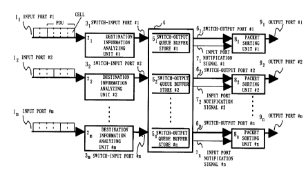
Referring now to the figure, the data switching
system has m number of input ports bearing reference
numerals llthrough 1" such as input ports #1, #2 and #m
through which ATM cells are inputted to the data switching
system, where m is a positive integer and this condition
is to be followed in the descriptions below. Reference
numerals 2lthrough 2,~ denote destination information
analyzing units such as destination information analyzing
units #1, #2 and #m. Each of the destination information
analyzing units analyzes destination information included
in a received ATM cell from a corresponding input port to
determine an output port through which the received ATM
cell is to be outputted from the data switching system.
Reference numerals 3, through 3,~ denote switch-input ports
such as switch-input ports #1, #2 and #m. The switch-input
ports 31 through 3m receive ATM cells through a destination
information analyzing operation performed by the
destination information analyzing units 2lthrough 2,~ to be
inputted to a cell switch, bearing a reference numeral 4.
The cell switch 4 performs a switching operation to sort
received ATM cells through the switch-input ports 31
through 3W based upon the output port determined through
the destination information analyzing operation. Reference
CA 02313683 2000-07-07
13
numerals 51 through 5~ denote output queue buffer stores
provided in the cell switch 4 such as output queue buffer
stores #1, #2 and #n, where n is a positive integer and
this condition is to be followed in the descriptions below.
The output queue buffer stores 51 through 5" store sorted
cells temporarily to be outputted from the cell switch 4.
The output queue buffer stores 5, through 5n correspond
respectively to output ports. Reference numerals 61
through 6" denote switch-output ports such as switch-output
ports #1, #2 and #n through which the cell switch 4
outputs sorted cells queued in the output queue buffer
stores 51 through 5n. Reference numerals 71 through 7"
denote input port notification signals such as input port
notification signals #1, #2 and #n. The input port
notification signals 7,through 7n being outputted from the
cell switch 4 to identify the input port of an outputted
cell from the respective switch-output ports 6, through 6n
through which the outputted cell was inputted to the data
switching system. Reference numerals 8lthrough 8" denote
packet sorting units such as packet sorting units #1, #2
and #n for further sorting received sorted cells from the
switch-output ports 61 through 6" according now to input
port through which the received cells were inputted and
outputting sorted received cells in a packet. Reference
numerals 9lthrough 9n denote output ports such as output
CA 02313683 2000-07-07
- 14
ports #1, #2 and #n for outputting cells from the packet
sorting units or the data switching system.
Fig. 2 shows a schematic block diagram illustrating
the configuration of the output queue buffer stores 51
through 5n provided in the cell switch 4 which correspond
to the respective output ports 9lthrough 9~, one only of
which, bearing the reference numeral 51, is shown. Each of
the output queue buffer stores 51 through 5~ includes queue
buffer stores corresponding to the respective input ports
11 through 1".
Fig. 3 shows a schematic block diagram illustrating
the configuration of the packet sorting units 8lthrough 8"
one only of which, bearing the reference numeral 8,, is
shown. The packet sorting units #1 811s provided with a
packet sorting queue buffer store 101 and a VPI/VCI
replacing unit 111. The packet sorting queue buffer store
101 is provided with queue buffer stores corresponding to
the respective input ports. The VPI/VCI replacing unit 111
performs a VPI/VCI replacing operation of a VPI/VCI
provided within the header of each cell.
An operation of the data switching system of this
embodiment is now discussed.
It is assumed that the data switching system
according to this embodiment receives ATM cells of packet
data and AAL 5 is employed as a type of ATM Adaptation
CA 02313683 2000-07-07
Layer (AAL). With AAL 5, as shown schematically in Fig. 4,
flag is used for indicating a final cell. The flag is set
to the payload type (PT) bit of a final member cell of
each packet. The flag also identifies a gap between
5 packets of cells. Fig. 5 shows a typical incoming string
of cells to the data switching system through the
respective input ports 11 through 1m. As shown
schematically in Fig. 5, it is assumed that the data
switching system may receive through the respective input
10 ports 11 through 1,~ an intermingled or multiplexed string
of cells including cells of different packets to be
transmitted towards different output ports. However, the
data switching system never receive through the respective
input ports 1, through 1~ an intermingled or multiplexed
15 string of cells including cells of different packets to be
transmitted towards the same output port.
For example, it is assumed that a cell to be
transmitted towards the output port #1 9, arrives at the
input port #1 11 and inputted to the data switching system.
The inputted cell is then inputted to the destination
information analyzing unit #1 2, to be subjected to a
destination information analyzing operation so as to
identify an output port through which the inputted cell is
to be outputted from the data switching system. With the
output port being identified, the inputted cell is sent to
CA 02313683 2000-07-07
1 6
the cell switch 4.
The cell switch 4 stores the cell temporarily in the
output queue buffer store 51 which corresponds to the
output port #1 91 towards which the cell is to be
transmitted. Specifically, in the output queue buffer
store 5,, the cell is stored in a queue buffer store
corresponding to the input port #1 11 because the cell is
inputted to the data switching system through the input
port #1 11. The temporarily stored cell is then read out
from the queue buffer store to be outputted through the
switch-output port #1 61 to the packet sorting unit #1 81.
When the cell is outputted to the packet sorting unit #1 81,
the input port notification signal #1 7, is outputted to
notify the packet sorting unit #1 81 that the cell was
inputted to the data switching system through the input
port #1 11. This input port notification operation by the
input port notification signal #1 71 depends upon such a
cell sorting and storing method employed in the cell
switch 4 as sorted cells to be transmitted towards the
output port #1 91 in the output queue buffer store 51 are
further sorted according to corresponding input ports to
be stored in the queue buffer stores corresponding to the
respective input ports.
The output queue buffer stores 51 through 5" each are
provided with the queue buffer stores corresponding to the
CA 02313683 2000-07-07
17
respective input ports 11 through 1~. There are several
possible methods such as Round Robin Method for reading
out cells from the respective queue buffer stores
corresponding to the respective input ports 11 through lm
in each of the output queue buffer store 51 through 5n.
However, these possible methods for reading out cells may
accompany no specific restriction therewith. However, in
such a specific case of cells as they are inputted through
the same input port and have the same level of priority,
the cells should be read out according to an original
order in the queue so that the order of the cells is not
changed.
As shown schematically in Fig. 6, the cell, when
being inputted to the packet sorting unit #1 81 from the
switch-output port #1 61 is stored in the packet sorting
queue buffer store 10,. The packet sorting queue buffer
store 101 is provided with queue buffer stores
corresponding to the respective input ports. The cell is
stored in a queue buffer store corresponding to the input
port #1 11 because the cell is inputted to the data
switching system through the input port #1 11. The cell is
read out on a packet basis from the packet sorting queue
buffer store 101 only when all the member cells of a packet
meet in the packet sorting queue buffer store 101 to
complete the packet.
CA 02313683 2000-07-07
1 8
Completion of each packet with all the member cells
can be determined by observing the payload type (PT) bits
of incoming cells to see a final cell. As aforementioned,
a final cell identifies itself with the flag being
provided in the payload type (PT) bit. The cells being
read out from the packet sorting queue buffer store 101 on
a packet basis are subjected to a VPI/VCI replacing
operation performed by the VPI/VCI replacing unit 111 on a
packet basis. The packet sorting operation performed in
the packet sorting unit 81 is illustrated schematically in
Fig. 6. As illustrated in the figure, intermingled or
multiplexed cells in an incoming string to the packet
sorting queue buffer store 101 are sorted according to the
input port to be outputted in a sorted string of cells
including a final cell in a complete packet in a row. The
complete packet of cells are assigned a single VPI/VCI to
be transmitted. Thus, according to this embodiment, no
cells of different packets are intermingled in an
outputting string of cells from the packet sorting queue
buffer store 101, and therefore, the number of VPI/VCI
identifiers can be minimized.
The cell switch 4 performs a switching operation of
cells, the cell being of a fixed-length, on a cell basis.
This allows the data switching system to process data at a
high speed among two or more input/output devices. Because
CA 02313683 2000-07-07
19
the switching operation is performed on a cell basis, the
cell switch 4 still outputs an intermingled string of
processed cells of different packets through the
respective switch-output ports 61 through 6n in this stage,
the different packets of cells having been inputted to the
data switching system through different input ports 11
through 1,~. In the next stage, however, the packet sorting
unit #1 81, for example, receiving the intermingled string
of cells of different packets from the cell witch 4, sorts
the intermingled cells on a packet basis to obtain
complete packets of cells. The complete packet of cells
are outputted from the data switching system one by one
with a single VPI/VCI. This allows the single VPI/VCI to
be shared by different packets of cells which have been
inputted to the data switching system through different
input ports. In other words, the single VPI/VCI can be
used in a repeated manner among two or more packets of
cells one after another when being outputted from the data
switching system.
Thus, the data switching system according to this
embodiment includes the packet sorting units 8lthrough 8n
being placed at back of the cell switch 4, each of which
has such a queue buffer store as the packet sorting queue
buffer store 101 which is provided with the queue buffer
stores corresponding to the respective input ports 11
CA 02313683 2000-07-07
through 1,~ for sorting incoming cells according to the
input ports based upon the input port notification signals
7lthrough 7~ issued by the cell switch 4 for identifying
the corresponding input ports through which the individual
5 cells were inputted to the data switching system. This
allows the data switching system to output cells on a
packet basis in a row, which also allows the data
switching system to minimize a number of VPI/VCI
identifiers for an efficient data transmission.
Embodiment 2.
A second embodiment of the present invention
introduces a variation of the data switching system of the
first embodiment. According to the data switching system
of the first embodiment, the packet sorting units 81
through 8" sort cells according to the input ports based
upon the input port notification signals #1 71 through #n
7n, respectively, received from the cell switch 4, whereas
corresponding packet sorting units of the data switching
system of the second embodiment sort cells based upon
information which is added to individual cells for
identifying the respective input ports #1 11 through #m 1m
through which the cells have been inputted to the data
switching system.
The data switching systera of the second embodiment
CA 02313683 2000-07-07
2 1
is discussed below with reference to Figs. 7 and 8. Fig. 7
shows a block diagram of the data switching system
according to the second embodiment of the present
invention. Referring to the figure, reference numerals 121
through 12p denote input port information adding units such
as input port information adding units #l, #2 and #m. The
input port Information adding units 121 through 12,~ each
add input port information to inputted individual ATM
cells for identifying input ports through which the cells
are inputted to the data switching system. In Fig. 7, the
input port information adding units 121 through 12" are
placed in front of the destination information analyzing
units 21 through 2,~. However, the input port information
adding units 121 through 12,~ may alternatively be placed in
back of the destination information analyzing units 21
through 2,~. Further alternatively, the input port
information adding units 121 through 12,~ and the
destination information analyzing units 2lthrough 2,~ may be
combined in such a manner that an input port information
adding operation and a destination information analyzing
operation are performed in a combined unit. Reference
numerals 131 through 13m denote output queue buffer stores
provided in the cell switch 4 for storing incoming cells
in queues for the time being. The output queue buffer
stores 131 through 13,~ correspond to the respective output
CA 02313683 2000-07-07
- 22
ports 91 through 9n.
Reference numerals 141through 14" denote packet
sorting units such as packet sorting units #1, #2 and #n.
The data switching system of this embodiment is
characterized primarily with the packet sorting units 141
through 14". The packet sorting units 141through 14"
receive sorted cells outputted to the respective switch-
output ports 6lthrough 6" corresponding to the output ports
91 through 9". The packet sorting units 141 through 14"
further sort the sorted cells according to the
corresponding input ports based upon the input port
information which is added to individual cells at the
respective input port information adding units 121 through
12ro. The packet sorting units 141through 14" then sort
inputted cells on a packet basis.
Components other than those identified above of the
data switching system of this embodiment are to be
considered the same in function and configuration as the
components of the data switching system of the first
embodiment illustrated in Fig. 1 such as the input port 11
through 1~,, the destination information analyzing units 21
through 2,~, the switch-input ports 31 through 3,~, the cell
switch 4, the switch-output ports 61 through 6n, and the
output port s 91 through 9" .
Fig. 8 shows a block diagram of the packet sorting
CA 02313683 2000-07-07
23
units 141 through 14,~ of this embodiment one only of which,
bearing the reference numeral 141, is shown as an example.
The packet sorting unit 141 is provided with an input port
information analyzing unit 151, the packet sorting queue
buffer store 101 including a plurality of queue buffer
stores corresponding to the respective input ports 11
through 1,~ and the VPI/VCI replacing unit 111 for replacing
a VPI/VCI provided within the header of an ATM cell. The
packet sorting queue buffer store 101 and the VPI/VCI
replacing unit 111 are the same in function and
configuration as those of the packet sorting queue buffer
store 101 and the VPI/VCI replacing unit 111 of Fig. 1.
An operation of the data switching system according
to the second embodiment is now discussed in detail with
reference to Figs. 7 and 8.
Similarly to the first embodiment, it is assumed
that the data switching system of this embodiment receives
ATM cells of packet data. AAL 5 is employed as an ATM
Adaptation Layer in this embodiment. Cells of different
packets arriving at the data switching system through the
respective input ports 11 through 1,~ are not intermingled
or multiplexed in a single string on a cell basis if the
different packets are to be transmitted to the same output
port.
In the case that a cell to be transmitted toward the
CA 02313683 2000-07-07
- 24
output port #1 91 arrives at the data switching system
through the input port #1 11, the arriving cell is received
by the input port information adding unit #1 121 where the
input port information for identifying the input port #1 11
is added to the cell. The cell with the input port
information is transmitted to the destination information
analyzing unit #1 21 where the destination information of
the cell is analyzed to identify an output port through
which the cell is to be outputted from the data switching
system. The cell is then transmitted to the cell switch 4.
The cell switch 4 stores this cell temporarily in
the output queue buffer store #1 131 corresponding to the
output port #1 91 towards which the cell is to be
transmitted. The temporarily stored cell is then read out
from the output queue buffer store #1 131 and then inputted
to the packet sorting unit #1 141 through the switch-output
port #1 61. In the packet sorting unit #1 141, the cell is
inputted to the input port information analyzing unit 151
where the input port of the cell is determined and then
the cell is sent to the packet sorting queue buffer store
101. The packet sorting queue buffer store 101 is provided
with a plurality of queue buffer stores corresponding to
the respective input ports 11 through 1~. In the packet
sorting queue buffer store 101, the cell is stored in one
of the queue buffer stores corresponding to the input port
CA 02313683 2000-07-07
- 25
#1 11 because the cell was inputted through the input port
#1 11. In this manner, cells in the packet sorting queue
buffer store lOlare stored in appropriate queue buffer
stores corresponding to the respective input ports 11
through 1~ which are determined by the input port
information analyzing unit 151.
Then the cells are read out from the packet sorting
queue buffer store 101 on a packet basis only when the flag
of a final cell is detected so that all the member cells
of a packet are stored in a queue buffer store to complete
the packet. The cells read out from the packet sorting
queue buffer store 101 in a packet are then subjected to a
VPI/VCI replacing operation performed in the VPI/VCI
replacing unit 111. Cells are read out on a packet basis
from the packet sorting queue buffer store 101 so that a
VPI/VCI replacing operation is performed also with the
packet based cells on a packet basis in the VPI/VCI
replacing unit 111.
The cell switch 4 performs a cell based switching
operation for fixed-length cells. The cell switch 4 is
capable of high speed switching among two or more
input/output devices. Thus, cells are switched on a cell
basis so that cells of different packets inputted through
different input ports are outputted in an outputting
string in an intermingled or multiplexed manner at the
CA 02313683 2000-07-07
26
switch-output ports 61 through 6" corresponding to the
respective output ports 91 through 9". However, at the next
stage, in the packet sorting units 141 through 14", the
intermingled string of cells are sorted on a packet basis
so that the same VPI/VCI can be assigned to two or more
different packets of cells inputted through different
input ports to be outputted from the data switching system.
In other words, a VPI/VCI used for a packet of cells can
be reused in a repeated manner for a different packet of
cells when a former packet is outputted from the data
switching system.
Thus, the data switching system according to this
embodiment includes the packet sorting units 141through 14n
being placed at back of the cell switch 4. Each of the
packet sorting units 141through 14" has such a queue buffer
store as the packet sorting queue buffer store 101. The
packet sorting queue buffer store 101 is provided with the
queue buffer stores corresponding to the respective input
ports llthrough 1" for sorting incoming cells according to
the input ports based upon the input port information
added to the individual cells for identifying the
corresponding input ports through which the individual
cells were inputted to the data switching system. This
allows the data switching system to output cells on a
packet basis in a row, which also allows the data
CA 02313683 2000-07-07
27
switching system to minimize a number of VPI/VCI
identifiers for an efficient data transmission.
Embodiment 3.
A third embodiment of the present invention
introduces a data switching system having a plurality of
packet sorting units being placed at back of the
respective input ports. On the contrary to the packet
sorting units 8lthrough 8n being placed at back of the cell
switch 4 according to the data switching system of the
first embodiment, the plurality of packet sorting units of
this embodiment is placed before a cell switch. In
addition to that, the data switching system of the third
embodiment introduces an alternative inventive method for
outputting cells in order to minimize the number of
VPI/VCI identifiers.
Fig. 9 shows a block diagram of the data switching
system according to the third embodiment.
Reference numerals llthrough 1,~ denote m number of
input ports through which ATM cells are inputted to the
data switching system. Reference numerals 161through 16,~
denote packet sorting units such as packet sorting units
#1, #2 and #m which are coupled directly to the respective
input ports 11 through l,~ for receiving the ATM cells from
the corresponding input ports. The packet sorting units
CA 02313683 2000-07-07
28
161through 16~ determine output ports through which the
respective inputted ATM cells are to be outputted from the
data switching system, perform a VPI/VCI replacing
operation of the received ATM cells, sort the cells having
a VPI/VCI replaced according to the output ports, and then
output the sorted cells on a packet basis. In addition to
that, each of the packet sorting units 161through 16"
issues a transmission request signal on a packet basis of
the ATM cells and outputs a packet of the ATM cells upon
reception of a transmission enable signal in response to
the transmission request signal. Reference numerals 171
through 17" denote transmission request signals which are
transmitted from the respective packet sorting units 161
through 16~ in order tv request a permission for
transmitting a packet of ATM cells. Reference numerals 181
through 18,~ denote transmission enable signals which are
transmitted to the respective packet sorting units 161
through 16,~ in order to permit the transmission of the
packet of ATM cells in response to the transmission
request signal. Reference numerals 191through 19m denote
completion notifying signals which are transmitted from
the respective packet sorting units 161through 16,~ in order
to inform of a completion of transmitting the packet of
ATM cells upon completion of the transmission of the
packet of ATM cells. Reference numerals 3lthrough 3,~
CA 02313683 2000-07-07
29
denote switch-input ports through which the sorted packet
based ATM cells are inputted to a cell switch 4B.
The cell switch 4B is provided with an arbitration
unit 20 and a cell switching unit 21. The arbitration unit
20 performs an arbitration operation of transmission
requests by means of the transmission request signals 171
through 17~ sent from the respective packet sorting units
161through 16" so as to permit the respective packet
sorting units 161through 16~ to transmit a packet of cells
in response to selected ones of the transmission request
signals 171through 17~, by transmitting the transmission
enable signals 181through 18". In addition to that, the
arbitration unit 20 controls the cell switching unit 21 by
means of a switch control signal 22. The cell switching
unit 21 is controlled by the arbitration unit 20 to output
packets of cells to appropriate switch-output ports.
Reference numerals 9lthrough 9n denote the output ports
through which the data switching system outputs and
transmits packet based sorted cells. According to the data
switching system of this embodiment, the switch-output
ports are equated to the output ports 9lthrough 9".
Fig. 10 shows a block diagram of the packet sorting
units 161through 16,~, one only of which, bearing the
reference numeral 161, is shown as an example. The packet
sorting unit 161 is composed of an output port
CA 02313683 2000-07-07
' 30
determination unit 23, a VPI/VCI replacing unit 24, an
output queue buffer store 26 and a control circuit 25. The
output queue buffer store 26 is provided with a plurality
of FIFO (First-in First-out) memories corresponding
respectively to the output ports 9lthrough 9~.
An operation of the data switching system of this
embodiment is now discussed.
Similarly to the data switching system of the first
embodiment, it is assumed that the data switching system
of this embodiment receives ATM cells of packet data. AAL
5 is employed as an ATM Adaptation Layer. It is also
assumed that ATM cells of different packets can be
intermingled or multiplexed on a cell basis in an
inputting string to the data switching system through the
respective input ports 11 through 1~ only if the ATM cells
of different packets are not to be transmitted towards the
same output port. In other words, ATM cells of different
packets to be transmitted towards the same output port
cannot be intermingled or multiplexed on a cell basis in a
single inputting string.
In the case that an ATM cell arrives at the input
port #1 1, and the ATM cell is to be transmitted towards
the output port #1 91, the ATM cell is first sent to the
packet sorting unit #1 161. In the packet sorting unit #1
161, the cell is inputted to the output port identifying
CA 02313683 2000-07-07
31
unit 231 where an output port through which the ATM cell is
to be outputted from the data switching system 1s
determined. Then the ATM cell is inputted to the VPI/VCI
replacing unit 241 where the value of the VPI/VCI of the
ATM cell is replaced. The ATM cell is then stored in the
output queue buffer store 261 temporarily. In the output
queue buffer store 261, the ATM cell is stored in an
appropriate one of the FIFO memories corresponding the
output port 91. The FIFO memory receives and stores member
cells of a packet of which the ATM cell is a member one
after another. When all the member cells of the packet
meet in the FIFO memory or the output queue buffer store
261 with a detection of the flag indicating a final cell,
then the control circuit 251 issues a request for
permitting the transmission of a complete packet of the
ATM cells by transmitting the transmission request signal
#1 171. The control circuit 251, upon reception of a
permission of the transmission of the complete packet of
the ATM cells by means of the transmission enable signal
#1 181, controls the output queue buffer store 261 to
output the complete packet of ATM cells from the FIFO
memory. When all the member cells of the complete packet
are outputted from the output queue buffer store 261, then
the control circuit 251 notifies the cell switch 4B of the
completion of the transmission of the packet of cells by
CA 02313683 2000-07-07
32
transmitting the completion notifying signal #1 191.
An operation of the arbitration unit 20 provided in
the cell switch 4B is now discussed with reference to Figs.
11 through 16. The data switching system of this
embodiment is primarily characterized with the arbitration
unit 20 which employs an arbitration logic for a
simultaneous switching operation of two or more packets
outputted from a plurality of the packet sorting units 161
through 16,~ with no cells of different packets Intermingled
in an outputting string. The cell switching unit 21
provided in the cell switch 48 has a function of a cross-
over type switch. Figs. 11 through 16 show an operational
series of arbitration performed by the arbitration unit 20
together with the respective packet sorting units #1 161,
#2 162 and #3 163 and the cell switching unit 21.
Referring now to Fig. 11, the switching unit 21 has
inputs 1, 2 and 3 corresponding respectively to the
switch-input ports #1 31, #2 32 and #3 33 and outputs 1, 2
and 3 corresponding respectively to the output ports #1 91,
#2 92 and #3 93. Cells stored in the respective FIFO
memories of the output queue buffer stores 261, 26z and 263
are labeled with f, m or a for distinguishing a front cell,
a middle cell, or an end or final cell, respectively. The
cells are also distinguished by labeling numerals 1, 2 and
3 for identifying output ports #1 91, #2 9a and #3 93
CA 02313683 2000-07-07
33
towards which the cells are to be transmitted. Accordingly,
a cell being labeled with a sign m:l, for example, is one
of middle cells of a packet which is to be transmitted
towards the output port #1 91 corresponding to the output 1
of the cell switching unit 21. Fig. 11 shows a situation
when the arbitration unit 20 receives a plurality of the
transmission request signals 171through 17p at one time.
According to the figure, the packet sorting unit #2 162
receives an end cell to complete a packet which is to be
transmitted towards the output port #1 9, stored in an FIFO
memory corresponding to the output port #1 91 in the output
queue buffer store 262 and the packet sorting unit #3 163
also receives an end cell to complete a packet which is to
be transmitted towards the output port #3 93 stored in an
FIFO memory corresponding to the output port #3 93 in the
output queue buffer store 263. Then the control circuits
25a and 253 transmit the transmission request signals 172
and 173 respectively to the arbitration unit 20 at the same
time.
Fig. 12 shows an arbitration operation of the
arbitration unit 20 in response to the transmission
request signals 172 and 173. The arbitration unit 20
transmits the transmission enable signal 182 to the packet
sorting unit #2 16z to permit a transmission of the packet
to be transmitted towards the output port #1 91 and also
CA 02313683 2000-07-07
34
the transmission enable signal 183 to the packet sorting
unit #3 163 to permit a transmission of the packet to be
transmitted towards the output port #3 93. In addition to
that, the arbitration unit 20 instructs the cell switching
unit 21 to output the packet of cells which will be
received through the input 2 to the output 1 and to output
the packet of cells which will be received through the
input 3 to the output 3. Accordingly, the cell switching
unit 21 performs a cell switching operation in compliance
with the instruction of the arbitration unit 20 so as to
output a string of cells of the packet to be transmitted
towards the output port #1 91 to the output 1 and a string
of cells of the packet to be transmitted towards the
output port #3 93 to the output 3.
Figs. 13 through 16 show a series of an arbitration
operation performed by the arbitration unit 20 to deal
with another case. Referring now to Fig. 13, two end cells
'of different packets, one to be transmitted towards the
output port #1 91 and the other to be transmitted towards
the output port #2 92, arrive in a row at the packet
sorting unit 161 during which the outputs 1 and 2 of the
cell switching unit 21 are used for transmitting the
packets of cells from the packet sorting units 16a and 163
respectively. An arriving cell to be transmitted towards
the output port #1 91 is inputted to an FIFO memory
CA 02313683 2000-07-07
corresponding to the output port #1 91 to complete a packet
of cells in the output queue buffer store 261. Accordingly,
the control circuit 251 transmits the transmission request
signal 171 for transmitting the packet of cells to be
5 transmitted towards the output port #1 91 to the
arbitration unit 20 as shown in Fig. 14. The arbitration
unit 20 receives the transmission request signal 171.
However, a path towards the output 1 is used by outputting
the packet of cells received from the packet sorting unit
10 162 through the input 2 of the cell switching unit 21.
Then, in this situation, the arbitration unit 20 gives no
permission for transmitting the packet of cells to be
transmitted towards the output port #1 91. The arbitration
unit 20 can issue the transmission enable signal 181 only
15 after the currently outputting operation of the packet of
cells to the output 1 is completed.
On the other hand, as shown in Fig. 15, the other
end cell to be transmitted towards the output port #2 92 is
inputted to an FIFO memory corresponding to the output
20 port #2 92 to complete a packet in the output queue buffer
store 261. The control circuit 251 then outputs the
transmission request signal 171 for transmitting this
packet of cells to be transmitted towards the output port
#2 92. In this situation, no packet of cells uses a path
25 towards the output 2 in the cell switching unit 21 so that
CA 02313683 2000-07-07
36
the arbitration unit 20 gives a permission of transmitting
outputting the packet to be transmitted towards the output
port #2 9a to the packet sorting unit #1 161. As a result,
as shown in Fig. 16, the packet of cells to be transmitted
towards the output port #2 9z is outputted from the packet
sorting unit #1 161 to the switching unit 21 through and
then outputted from the cell switching unit 21 through the
output 2.
As aforementioned, the data switching system of this
embodiment having the packet sorting units 161through 16~
being placed at back of the input ports llthrough h sorts
received ATM cells of different packets inputted through a
single input port to complete a packet of ATM cells,
switches the ATM cells on a packet basis and outputs the
complete packet of ATM cells in a row to the plurality of
output ports. Therefore, the cell switch 4B receives a
packet based incoming string of sorted ATM cells being
ready for transmission from the respective packet sorting
units 161through 16~. In other words, the cell switch 4B
receives no intermingled or multiplexed string of ATM
cells inputted through various input ports which are to be
transmitted towards a single output port. For this reason,
a VPI/VCI can be used for two or more packets of ATM cells
to be transmitted from the data switching system in a
repeated manner. In addition to that, two or more packets
CA 023136832000-07-07
37
of cells can be switched to be outputted at one time if
the packets are not to be transmitted through the same
output port.
Thus, the data switching system of this embodiment
is characterized with the packet sorting units 161through
16,~ placed before the cell switch 4B and the arbitration
unit 20. The arbitration unit controls the cell switching
operation of the cell switching unit 21 so as to output
packets of cells in a well organized manner.
The invention being thus described, it will be
obvious that the same may be varied in many ways. Such
variations are not to be regarded as a departure from the
spirit and scope of the invention, and all such
modifications as would be obvious to one skilled in the
art are intended to be included within the scope of the
following claims.