Note: Descriptions are shown in the official language in which they were submitted.
CA 02313925 2000-07-17
TUNABLE BANDPASS FILTER
FIELD OF THE INVENTION
The present invention relates to microwave filters in wireless
telecommunications
systems. In particular, the present invention relates to dielectric resonator
filters operating in
microwave and millimeter wave rectangular waveguides or cavities of
transceivers.
BACKGROUND OF THE I~1VENTION
Over the years a wide variety of microwave and millimeter wave filters have
been
developed, each satisfying specific application requirements but none offering
the optimum
combination of low insertion loss, higher order mode rejection, high unloaded
Q factor, high
temperature stability, reduced filter size, tunability, and ease of
manufacturing.
The first-generation filters consisted of empty cascaded conductive cavities
connected
together and separated by metallic walls with iris-controlled couplings. These
filters are bulky
and not particularly suitable for use at low frequencies such as those below
the X-band. One
solution to this problem was the construction of a coaxial structure
supporting a TEM mode with
a capacitive gap called a comb-line, as described in G.L. Matthaei, "Comb-line
Bandpass Filters
of Narrow or Moderate Bandwidth", Microwave Journal, Vol. 6, August 1963.
While this
technology offers a greater reduction in size compared to the size of empty
rectangular or
cylindrical cavities, its moderate Q factor does not meet the stringent Q
factor specifications
required in certain modern telecommunication systems.
To obtain a high Q factor, the filter configurations most commonly used in
today's
telecommunication systems consist of a dielectric puck mounted inside a
conductive housing
without touching the metal conductor, as described in the following
references: (a) J.F. Liang and
W.D. Blaire, "High Q TEo, Mode DR Filters for PCS Wireless Base Stations",
IEEE
Transactions, Microwave Theory Tech., Vol. 1, MTT-46, Dec. 1998; (b) X-P Liang
and K.A.
Zaki, "Modeling of Cylindrical Dielectric Resonators in Rectangular Waveguides
and Cavities",
IEEE Trans. Microwave Theory Tech., Vol. MTT-4l,Dec. 1993: and (c) US Patent
5,777,534
to Harrison et al., entitled "Inductor Ring for Providing Tuning and Coupling
in Microwave
Dielectric Resonator Filters". In these structures the electromagnetic field
is concentrated inside
-1-
CA 02313925 2000-07-17
the puck and vanishes gradually outside. While the relatively wide cavity used
in these structures
reduces the ohmic loss on the metallic wall and increases the Q factor, it
also increases the size
and weight of the filter. Moreover, an undesirable electromagnetic mode
(called the HE"",8 mode)
is excited in such structures. This mode produces spurious responses close to
the filter
bandwidth, which affects the filter rejection performance.
With the advent of cellular mobile phone systems, new filter technologies
using dielectric
materials have been developed which yield moderate Q factors and reduced size,
such as that
described in Kikuo Wakino et al, "Miniaturization Technologies of Dielectric
Resonator Filters
for Mobile Communications", IEEE Trans. Microwave Theory Tech., Vol. MTT-42,
July 1994.
However, the topology of the majority of these technologies involve complex
geometry that
requires high machining accuracy and increased assembly time.
Other recent technologies have been developed to reduce spurious response. A
simple
configuration of such schemes has been proposed by A. Abdelmonem, J-F. Liang
and K.A. Zaki,
"Full-wave Design of Spurious-free DR TE Mode Bandpass Filters", IEEE Trans.
Microwave
1 S Theory Tech., Vol. MTT-43, April 1995. While the spurious response in this
structure is
substantially free, the resonators are not tunable. They also require high
machining tolerance and
high precision in the selection of the value of the dielectric constant.
An example of a prior art device tuning arrangement for a dielectric resonator
filter 40
is illustrated in Fig. 1. The filter 40 includes a metallic disk 42 attached
to the upper surface of
a housing structure 44 by a screw 46. A dielectric resonator 48 is mounted on
a support 50
centrally positioned within a cavity 52 of filter 40. The distance between the
top surface of the
resonator 48 and the bottom surface of the disk 42 can be varied up and down
by rotating the
screw 46. The disk 42 interacts with the magnetic field of the resonator 48
causing perturbation
of the resonance frequency of the cavity 52. A disadvantage of this Topology
is the excitation
of undesirable spurious hybrid modes at frequencies that are close to the
filter's passband.
It is therefore desirable to provide a substantially smaller-size filter for
both microwave
and millimeter wave frequency bands that uses internally-tunable dielectric
resonators. It is
further desirable to provide dielectric resonators that have a high Q factor,
are easily
manufactured and mounted, and provide substantial improvement in out-of band
hybrid mode
rejection performances.
-2-
CA 02313925 2000-07-17
SUMMARY OF THE INVENTION
It is an object of the present invention to obviate or mitigate at least one
disadvantage of
prior art bandpass filters. In particular, it is an object of the present
invention to provide a
dielectric resonator filter, particularly for microwave and millimeter wave
applications, that is
tunable.
In accordance with a first aspect of the present invention , there is provided
a tunable
dielectric resonator filter. The tunable dielectric resonator filter consists
of an electrically
conductive housing defining a cavity, and a dielectric resonator disposed in
the cavity. A tuning
aperture is formed in the resonator. The aperture is substantially parallel to
a direction of an
electric field excited within the resonator. A tuning device, such as a rod or
screw, received
within the tuning aperture. The depth of penetration of the tuning device
within the resonator
determines a frequency response of the resonator.
Typically, a coupling probe is provided to couple a signal to and from the
cavity. The
coupling probe excites the cavity in a TE mode, and can be within the cavity
or disposed in a
coupling aperture provided in the resonator. The filter of the present
invention in effectively
excited in a LSE mode. The resonator can be provided with an electrically
conductive coating,
on any of its top, bottom or side surfaces.
By coupling together a series of dielectric resonator filters according to the
present
invention, a tunable bandpass filter can be formed. Typically, the coupling is
achieved by irises.
Alternatively, an oscillator can be formed by coupling together a dielectric
resonator filter
according to the present invention with an oscillating element.
BRIEF DESCRIPTION OF THE DRAWINGS
Preferred embodiments of the present invention will now be described, by way
of
example only, with reference to the attached Figures wherein:
Figure 1 is a side view of a prior art filter;
Figure 2 is a top view of a six-pole, dielectric resonator filter in
accordance with the
present invention;
Figure 3 is a cross-sectional view of the dielectric resonator filter shown in
Figure 2;
-3-
CA 02313925 2000-07-17
Figure 4 is a top view of a filter cavity showing the unloaded and loaded
sections of a
rectangular resonator;
Figure 5 is a top view of a filter cavity showing the unloaded and loaded
sections of a
cylindrical resonator;
Figure 6 is a cross-sectional view of Figure 4 or Figure 5 showing the
uniformity of the
dielectric resonator geometry in the direction of the electric field;
Figure 7 is a cross-sectional view of the input/output coupling section of a
filter having
a shorted coupling rod positioned outside the dielectric resonator in
accordance with the present
invention;
Figure 8 is a cross-sectional view of the input/output coupling section of a
filter having
an open-ended coupling rod positioned outside the dielectric resonator in
accordance with the
present invention;
Figure 9 is a cross-sectional view of the input/output coupling section of a
filter having
an open-ended coupling rod positioned within the dielectric resonator in
accordance with the
1 S present invention;
Figure 10 is a cross-sectional view of a filter having two open-ended cross-
coupling rods
between two non-adjacent dielectric resonators in accordance with the present
invention;
Figure 11 is a perspective view of a dielectric resonator inserted in a
rectangular metallic
housing in accordance with the present invention;
Figure 12 is a perspective view of a dielectric resonator inserted in a
rectangular metallic
housing showing a small air gap between the top of the resonator and the top
of the housing;
Figure 13 is a cross-sectional view of a dielectric resonator inserted in a
rectangular
metallic housing showing the insertion of an expandable conductor slab in the
air gap of Fig. 12;
Figure 14 is a perspective view of a rectangular dielectric resonator that has
been metal-
plated on its top and bottom surfaces;
Figure 1 S is a perspective view of a rectangular dielectric resonator that
has been metal-
plated only on its bottom surface in accordance with another aspect of the
present invention.
Figure 16 is a perspective view of a cylindrical dielectric resonator that has
been metal-
plated on its top and bottom surfaces;
Figure 17 is a perspective view of a cylindrical dielectric resonator that has
been metal-
-4-
CA 02313925 2000-07-17
plated only on its bottom surface;
Figure 18 is a top view of a filter showing the longer-spaced coupling between
two
adjacent rectangular resonators without an iris coupler;
Figure 19 is a top view of a filter showing the longer-spaced coupling between
two
adjacent cylindrical resonators without an iris coupler;
Figure 20 is a top view of a filter showing the shorter-spaced coupling
between two
adjacent rectangular resonators with an iris coupler;
Figure 21 is a top view of a filter showing the shorter-spaced coupling
between two
adjacent cylindrical resonators with an iris coupler;
Figure 22 is a perspective view of a rectangular resonator with partial
metallic plating on
one of its lateral sides;
Figure 23 is a perspective view of a cylindrical resonator with partial
metallic plating on
its cylindrical surface;
Figure 24 is a top view of a filter showing rectangular and cylindrical
resonators adjacent
to one another;
Figure 25 is a top view of a filter showing two similar rectangular resonators
positioned
90° from one another;
Figure 26 is a graph showing the measured insertion loss and return loss
responses of a
reduced-size filter constructed in accordance with the present invention;
DETAILED DESCRIPTION OF THE INVENTION
Generally, the present invention provides a tunable dielectric resonator
filter operating
in a LSE,°a mode. The filter of the present invention is substantially
reduced in size and weight
when compared to prior art TE°,a filters. Further, it is much easier to
tune than prior art dielectric
resonator filters, while still satisfying the desired requirements of low
insertion loss, good out-of
band rej ection performance, relatively large unloaded Qs, high-temperature
stability, and ease
of manufacturing and mounting.
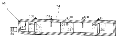
Referring now to Fig. 2 and Fig. 3, there is shown a top view and a cross-
sectional view
of a six-pole, dielectric resonator filter 60 according to one aspect of the
present invention,
including six resonant cavities 62, 64, 66, 68, 70 and 72 housed within the
metallic walls of a
-5-
CA 02313925 2000-07-17
rectangular waveguide structure 74. External coupling of the filter is
performed by the coupling
devices 76, 78 and 80,82, whereas internal coupling between cavities is
performed by the irises
84, 86, 88, 90, and 92 and by the cross coupler 94. Rectangular-shaped
dielectric resonators 96,
98, 100, 102, 104 and 106, having a high dielectric constant and high
intrinsic Q, are positioned
centrally within their respective cavities and flush with the top and bottom
walls of the metallic
structure 74, as shown in Fig. 3. Substantially central to each dielectric
resonator and in the same
direction as the electric field (y-axis) is an opening that penetrates the
entire resonator, allowing
for the insertion of metallic or dielectric tuning screws (or rods) 108, 110
and 112.
Noted that no relative dimensional information should be inferred from these
figures, that
a smaller or greater number of cavities may be used according to the frequency
selectivity
requirements of the filter and according to the teachings of the present
disclosure, and that
alternative forms or shapes of the dielectric resonator, such as puck-shaped
disks, may be used.
Considering now the structural configuration of the preferred embodiment of
Fig. 2, the present
invention will be described by way of the electromagnetic signal that
propagates through the
1 S cavities and by showing how certain characteristics of the derived
equations allow for a wide
range of trade-off possibilities between the Q factor and the structural
dimension.
Due to the geometry of the metallic waveguide structure 74 and the orientation
of the
coupling probe 82 of Fig. 3, the signal propagating in the unloaded section of
the cavity (as
shown at 118 of Figs. 4, 5 and 6), operates in the standard TEo, mode. With
the common factor
e'"'' removed, the components of the electromagnetic field of the signal are
given by the super-
positioning of incoming and reflected TE"o modes as follows:
Ey = ~~I~ne Y"Z+,~Bn~neY"Z
n n
Hx J ~ F 'yn ~n a Y"Z ~ Bn Yn ~n eY"Z
~~0 n n
H~ _ .1 ~F y ~e_r"z +~By ,er"=
n n n n
~~0 n n
where
z
_ _n ~c _ z ~n ~as~ n ~ xl and Vin' = a n
yrt - ~ ~ ~ Iu0 ~0 ~ a VX
Q
CA 02313925 2000-07-17
However, as the signal propagates through the loaded section of the cavity,
the
components of the electromagnetic field are altered due to the super-
positioning of the incoming
and reflected LSEmo modes. In the section loaded with a rectangular dielectric
resonator (as
shown at section 120 of Fig 4), the components of the electromagnetic field
are given by the
following equations:
~.u __ Fri1~~ e-r~= + B°~~~ e~mz
y ~ m Y'm ~ mY'm
m m
Hs' - J ~Fm rm~me rmz ~Bm'~m~mermz
~~0 m m
Hz' - J ~ Fm ~m'e rmz ~ Bmf ~m'ermz
~~0 m m
Where
_ yT m
~m -
yrm = sin xim ~ a 2 d ~ cos(,~2mx~ for x <
~m - cOS x2m ~ ~ ~ sln xim ~ a x d
2 2 forx> 2
Similarly, in a section loaded with a cylindrical dielectric resonator (as
shown at 121 of
Fig. 5) the components of the electromagnetic field are given by the following
equations:
E'',' _ ~ Fn','Zm (kr)cos(m B)
m
Hs' _ ~~o ~ ~F,~'Zm(kr~sin(m9~
HZ' _ ~~o ~F,~ k Z~m(kr~cos(mB)
CA 02313925 2000-07-17
where
Zm(kr)= fm J",(kr)+Yrn(kr)
is a linear combination of Bessel and Neumann functions of the order n.
In the second and third sets of the above equations (for the loaded sections),
the values
of the constants x,m , x,m , rm and Fm are generally obtained by satisfying
the continuity
conditions of the field on the air/dielectric interfaces and the boundary
conditions of the lateral
conductor walls. While these parameters vary according to the cavity width,
the permitivity of
the loaded section, and the dielectric resonator width, they do not depend on
the resonator height.
It follows therefore that, due to the uniformity of the electric field in the
y axis (as shown in Fig.
6), the performance response of the filter regarding the central frequency,
bandwidth, and return
loss is not affected by changing the height of the filter. Thus, the
structural configuration of the
present invention (Fig. 2) allows for a wide range of trade-off selections
between the Q factor and
the filter dimension, and it can be shown that, while remaining well within
the imposed
selectivity limits, a nominal drop in the Q factor can result in an
appreciable reduction in
resonator size. This characteristic feature of height independence along the y-
axis of tunable
dielectric resonators is unique to the present invention.
Considering again the structural configuration of the presently preferred
embodiment of
the present invention (Fig. 2), it can be seen that the resulting uniformity
of the electrical field
along the y-axis allows for holes 122, 124 and 126 to be bored parallel to the
y-axis and
substantially central to, and within, the dielectric resonators. Said holes
allow for the insertion
of conductive or dielectric screws (or rods) 108,110 and 112. Upward or
downward adjustment
of these tuning devices causes perturbation of the electric field distribution
Ey'I of the mode
propagating within the respective resonators which, in turn, allows for an
appreciable shift in
frequency and good tuning of the filter. This internal method for tuning the
dielectric resonator
is unique to this invention.
Additional tuning of the filter is also made possible under the preferred
embodiment as
shown in Fig.3. The tuning devices 128 and 130 are positioned centrally
between adjacent
dielectric resonators. Upward or downward adjustment of these tuning devices
causes
perturbation of the electromagnetic field distribution in the TE"o mode
propagating between the
resonators which, in turn, allows for tuning of the filter.
_g_
CA 02313925 2000-07-17
In the preferred embodiment of the present invention the input and output
coupling,
shown in the unloaded sections 62 and 72 of Fig. 2 and Fig. 3, are performed
by a shorted rod
78 or 82 as shown in Fig. 7, or by an open rod 132 as shown in Fig. 8. Since
this coupling occurs
below the cut-off region of the waveguide section, it has less coupling
efficiency. This coupling
S method is better suited for narrow band filter applications.
However, in accordance with another aspect of the present invention, a
stronger coupling
is made possible for wider band filter applications by inserting the coupling
rod 134 through a
hole 136 within the dielectric resonator, as shown in Fig. 9. This coupling
method is much more
efficient than those shown in Fig. 7 and Fig. 8 because the coupling rod 134
is positioned
substantially within the concentrated portion of the electrical field.
In yet another embodiment of the present invention, a dual probe 94 is
inserted between
two non-adjacent dielectric resonators, as shown in Fig. 10. Due to the
available space between
the dielectric resonator and the lateral wall of the filter, the insertion of
a probe within said open
space allows for negative cross-coupling between the two non-adjacent
resonators. To avoid
shorting, the probe 94 is isolated by the dielectric material 138.
Additionally, the resonator cross-
coupling can be made tunable by connecting the probe 94 to a tuning screw 140,
as shown in Fig.
10. Upward or downward adjustment of the tuning screw causes a change in probe
position
between the two non-adjacent resonators, which, in turn, alters the cross-
coupling.
Alternatively, positive cross-coupling between the two non-adjacent dielectric
resonators
can be achieved by simply opening a small iris in the lateral wall facing the
two non-adjacent
resonators.
In the presently preferred embodiment of the present invention, the top and
bottom of the
resonators are in perfect contact with the top and bottom walls of the
waveguide structure 74, as
shown in Fig 11. The key advantages of this aspect of the invention are that
(a) it avoids
propagation of spurious hybrid modes within the filter, (b) it permits
reduction in filter size
(height independence), and (c) it provides for good thermal conductivity. To
achieve a good
contact between the resonator and the waveguide walls, the top and bottom of
the resonator are
plated with a conductive material such as silver or copper or other metallic
material, as shown
by the metal strips 146 and 148 of Fig. 14 and Fig.16.
The disadvantage of the tight-fitting configuration of Fig. 11 is that it
requires high
-9-
CA 02313925 2000-07-17
machining accuracy. To reduce this constraint in topology, an alternative
embodiment of the
present invention is proposed by introducing a small air gap 142 between the
top of the dielectric
resonator and the top wall of the waveguide structure 74, as shown in Fig. 12.
For a small gap,
the equations given above remain basically unaltered if the permitivity is
changed by the
effective corrective value, and the propagated mode in the loaded section
merely changes from
a pure LSE mode to a quasi LSE mode. Thus, for the same frequency application,
the drawback
resulting from this alternative embodiment is a slight increase in the width
of the dielectric
resonator and the introduction of a small amount of hybrid mode propagation.
However, in
accordance with a filrther aspect of the present invention, this drawback can
be rectified by filling
the air gap 142 with an expandable conductive slab 144, as shown in Fig. 13.
In the presently preferred embodiment of the present invention, the coupling
distance
between adjacent dielectric resonators can be reduced by the classic prior art
method of inserting
irises 150 or 152 between rectangular dielectric resonators 151 or cylindrical
dielectric resonators
153, as shown in Fig. 20 and Fig. 21. Figs. 18 and 19 show respective
dielectric resonators 151
and 153 without coupling irises. In single-mode filter designs, such a
coupling method is
required in order to reduce the otherwise wide spacing between adjacent
resonators. In yet
another aspect of the present invention, it is proposed to reduce the coupling
distance between
resonators even fiirttler by partially plating one lateral face 154 or 156 of
the dielectric block with
silver, copper, or other metallic material, as shown in Fig. 22 and Fig. 23.
In accordance with yet another aspect of the present invention, it is proposed
to use
different resonator shapes 151 and 153 or to rotate adjacent resonators
90° from one another, as
shown in Fig. 24 and Fig. 25. Depending on the permitivity, dimension, and/or
shape of the
dielectric resonator, the second mode LSE Zo, can vary between 1.2 and 2.5
times the "central
frequency" of the filter. Therefore, by changing the configuration of the
resonators as shown in
Fig. 24 or Fig. 25, the propagation of this mode can be substantially reduced.
Fig. 26 shows the measured frequency response of a reduced-size filter
constructed in
accordance with the preferred embodiment of the present invention (Fig. 2).
The two s-parameter
curves illustrate the excellent performance of the filter in comparison with
the larger-sized comb-
line or cylindrical-puck dielectric filters of the prior art.
As will be understood by those of skill in the art, the present invention
provides the
- 10-
CA 02313925 2000-07-17
ability to tune a dielectric resonator filter operating in a LSE,°a
mode by the simple expedient of
tuning screws or rods. The present invention can provide either positive or
negative tunable
cross-coupling between at least two non-adjacent dielectric resonators in a
rectangular waveguide
filter. Ideally, the dielectric resonators of the present invention are flush
with the upper and lower
walls of the metallic waveguide housing. However, by removing the metal from
one of the
resonator's surface and introducing a small air gap between the top of the
dielectric resonator and
the top wall of the waveguide structure, the manufacturing and mounting
process can be
simplified without compromising performance. Further, the coupling distance
between adjacent
dielectric resonators can be significantly reduced by partially plating one
adjacent face of the
dielectric block with conductive metallic material. Equally, enhanced
performance can be
achieved by using different resonator shapes or rotating adjacent resonators
90° from one another
in order to reduce the propagation of spurious hybrid modes.
The above-described embodiments of the invention are intended to be examples
of the
present invention. Alterations, modifications and variations may be effected
in the particular
embodiments by those skilled in the art, without departing from the scope of
the invention which
is defined solely by the claims appended hereto.
-11-