Note: Descriptions are shown in the official language in which they were submitted.
CA 02313951 2000-07-07
p2.txt
A Scheme for Accelerating Bit Line Equalization
in a High Speed DRAM Architecture
by Paul W. DeMone, June 6, 2000
A) Problem
The bitline equalization and precharge portion of a DRAM row
access cycle represents operational overhead that increases
the average latency of memory operations and reduces the rate
at which row accesses can be performed. Part of the difficulty
in reducing this dead time is due to typical DRAM architectures
which maximimize memory capacity per unit area by favouring
large DRAM cell arrays. Long and highly capacitive bitlines
require a relatively large amount of current to quickly change
the voltage on them. At the same time the width of large DRAM
arrays requires the simultanous precharge and equalization of
thousands of bit lines. The large number of active bitlines
limits the drive strength of precharge and equalization devices
for individual bit line pairs to avoid difficulties associated
with large peak aggregate currents.
New DRAM architectures for embedded applications often focus
on performance rather than bit density. This is achieved by
increasing the degree of subdivision of the overall memory
into a larger number of sub-arrays. Smaller active sub-arrays
permit the use of higher drive, faster precharge and equaliz-
ation circuits than possible in commodity memory devices. But
this approach runs into fundamental limits to how much the
bitline equalization period can be shortened due to the distr-
ibuted resistive and capacitive parasitic characteristics of
the bitline material.
B) Previous Approaches
Traditionally the designers of commodity DRAM devices were
strongly focussed on achieving low cost per bit through high
aggregate bit density than higher memory performance. The
cell capacity of a two dimensional memory array increases
quadratically with scaling while the "overhead" area of bit
line sense amps, word line drivers, and X and Y address dec-
oders increases linearly with scaling. Therefore the focus
on memory density meant that commodity DRAM devices were
architected with sub-arrays as large as practically possible
despite its strongly negative effect on the time required to
perform bitline pre-charge and equalization (as well as cell
readout, sensing, and writing new values).
The latency impact of slow bitline equalization and precharge
Page 1
CA 02313951 2000-07-07
p2.txt
has traditionally been minimized by the creation of two diff-
erent classes of memory operations: bank accesses (full row
and column access) and faster page accesses (column access
only to a row left open from a bank operation). The efficacy
of page accesses in reducing average latency is due to the
statistical spacial locality in the memory access patterns
o~f many computing and communication applications, that is,
the strong probability that consecutive memory accesses will
target the same row.
But this architecture is undesirable for many applications
such as real-time control and digital signal processing that
value deterministic, or at least minimum assured levels of
memory performance regardless of the memory address access
pattern. One solution is to perform a complete row and column
access for every memory operation and automatically close the
row at the end of the operation. Unfortunately even the use
o-f a highly sub-divided, small sub-array DRAM architecture is
performance limited by the distributed RC parasitic character-
istics of the bit line material due to current DRAM design anc
layout practices.
C) Key Aspects of the Invention
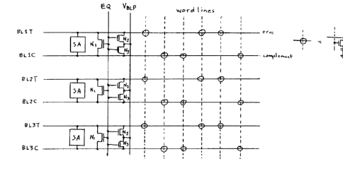
Current DRAM design and layout practices related to bitline
precharge and equalization are shown in Figure 1. The DRAM
array is composed of a number of pairs of bitlines each of
which share sense amplifiers and precharge equalization
circuitry. The DRAM may be arranged with all circuitry assoc-
iated with the bitlines on one side of the memory cell array
(lA) or with the peripheral circuitry for adjacent bitline
pairs distributed on opposite side of the array (1B).
Bitline precharge and equalization is performed by three n
channel transistors N1, N2, and N3. Nl helps to equalize the
voltage on the associated true and complementary bitline while
N2 and N3 drive the true and complementary bitline to the pre-
c,harge voltage level respectively.
During a DRAM access the bitline sense amplifiers SA sense
the voltage difference between the true and complementary
bitlines induced from the readout of the charge within the
accessed memory cell. The sense amp amplifies the difference
until the bitline with the higher voltage is raised close to
Vdd while the bitline with the lower voltage is pulled down
close to Vss. Common practice is for the bitline precharge
voltage Vblp to be set close to midway between Vdd and Vss.
Ideally only device Nl is needed because the precharge voltage
can be achieved by charge sharing between the true and compl-
Page 2
CA 02313951 2000-07-07
p2.txt
ementary bit line when the two are shorted through Nl. In
practice leakage, capacitive coupling, asymmetries in bitline
capacitance and other effects mean that some current must be
supplied through N2 and N3 to restore the bitline to Ublp.
D) The Invention
The difficulty involved in performing the bitline equalization
and precharge quickly is illustrated in Figure 2A. The necessary
circuitry, transistors Nl, N2, and N3, are located at one end
of a bitline pair. The bitlines have significant distributed RC
parasitics due to the minimum or near minimum width of the bit-
lines and the drain capacitance of the memory array access tran-
sistors attached to them. The time needed to equalize and pre-
charge a bit line pair is approximately proportional to the
square of the length of the bitline within the memory array.
The invention is the addition of an extra equalization transistor
N4 connected across each bitline pair as shown in Figure 2B. The
N4 device is located at the opposite side of the memory array as
the sense amplifier and traditional equalization devices. The add-
ition of the N4 device effectively halves the length of the bitline
as far as the RC delay is concerned and reduces the time needed to
perform bitline equalization and precharge time by about 75%. The
location of N4 is the key to the invention, not the extra drive N4
represents.
E) Design variations
The invention can be implemented for both DRAM architecture with
bitline peripheral circuitry located on one or both sides of the
memory sub-array as shown in Figure 3A and 3B respectively. An
alternative arrangement places the secondary bitline equalization
shorting transistor N4 in the middle of the array. In this case
the size of the primary shorting transistor Nl may be be greatly
reduced because it is only needed to compensate for the capacit-
ance of the sense amplifier and column access devices; the central
location of N4 is sufficient to cut the effective length of the
distributed RC delay of the bitlines in half. This variant is shown
in Figure 4A and 4B for both single sided and dual sided bitline
peripheral circuit arrangements respectively.
F) Other Applications
The invention can be applied to other situations where long pairs
of wires are used to transmit data either differentially or dual
Page 3
CA 02313951 2000-07-07
p2.tXt
rail, and the signal pair is equalized between data items. This
may include high performance SRAMs, other types of electronic
memories that are arranged in arrays, and long, high fanout data
buses within the datapaths of digital signal processors and micro-
processors.
Page 4