Note: Descriptions are shown in the official language in which they were submitted.
CA 02313992 2000-07-06
-1-
CALLING PARTY ANNOUNCEMENT MESSAGE MANAGEMENT
SYSTEM AND METHODS
BACKGROUND OF THE INVENTION
1. Field of the Invention
The present invention relates generally to the field of caller
identification devices and, specifically, to a method and apparatus for
detecting caller identification information and selecting predetermined
preferences responsive thereto.
2. Background Information
Over the past few years, the scope of telecommunications
services has broadened, allowing telephone companies to provide a
new variety of telephony offerings to subscribers. The most relevant
feature of the telephony offerings to embodiments of the present
invention is the caller identification service provided by the telephone
companies. With the caller identification service, the calling party's
telephone number is transmitted to the called party (assuming that the
calling party's telephone number is not blocked). The calling party's
telephone number is encoded in an incoming caller line identification
("ICLID") signal while the telephone of the called party is ringing. The
called party then captures the ICLID signal and decodes the calling
party's telephone number before picking up the telephone. This can be
done by installing a caller identification box, which may be purchased
from the telephone company or a telephone retail store, between the
telephone line and the telephone. Also, many telephones now have
the caller identification feature integrated therein. By using the caller
identification box to identify the calling party's telephone number, the
CA 02313992 2000-07-06
-2-
called party can "screen" calls. In addition, the caller identification box
displays and stores the telephone numbers) of those who have called,
while the called party is away from the telephone.
An improvement to the caller identification box is described in
United States Patent No. 5,526,406 ('406) entitled "Calling Party
Announcement Apparatus", issued to Luneau. The '406 patent relates
to an apparatus for providing the identity of the caller in synthesized
human speech in response to the ICLID signal provided by the
telephone company. After the called party has answered the telephone,
the calling party's name or telephone number is announced to the
called party over the telephone receiver. The called party can elect to
accept or reject the call before the telephone company central office has
connected the two parties together. However, the '406 patent has
several drawbacks including the use of synthesized human speech,
which has marginal voice quality and complicated signal processing
circuits and software to store and recall announcements.
SUMMARY OF THE INVENTION
The present invention comprises a caller identification method.
In one embodiment, the caller identification method includes detecting
an incoming telephone call, decoding a caller identification signal to
provide an incoming telephone number responsive to detecting the
incoming telephone call, and comparing the incoming telephone
number with one or more stored telephone numbers. The method
further includes performing one or more functions associated with a
stored telephone number if the incoming telephone number matches
the stored telephone number.
Other embodiments are described herein.
CA 02313992 2000-07-06
-3-
BRIEF DESCRIPTION OF THE DRAWINGS
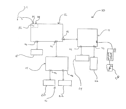
Figure 1 illustrates a block diagram of a telephone control system
according to one embodiment of the present invention.
Figure 2 illustrates a table of records contained within the
EEPROM of Figure 1 according to one embodiment of the present
invention.
Figure 3 shows each field of a record contained within the table.
Figure 4 shows the a timing diagram of an incoming caller line
identification signal transmitted between ring and call waiting signals.
Figure 5 illustrates a flow diagram of a process, according to one
embodiment of the present invention.
Figure 6 illustrates a block diagram of the recording and playback
device of Figure 1, according to one embodiment of the present
invention.
Figure 7 illustrates a block diagram of a portion of the SPI.
Figure 8 illustrates a mapping of control bits of the
configurations registers contained within the device.
Figure 9 shows the commands issued to the SPI for configuring
the device in the feed-through mode.
DETAILED DESCRIPTION
The present invention comprises a method and apparatus for
detecting and decoding an incoming caller line identification ("ICLID")
signal and selecting pre-determined preferences for call acceptance
responsive thereto. The telephone numbers of known callers are
/~.
CA 02313992 2000-07-06
-4-
stored in non-volatile memory in records. The incoming telephone
number is compared to the telephone numbers stored in the records.
Records are stored in no particular order at first, but once there is a
match, the records are ordered in descending order of frequency. Each
record includes a preference field indicating the action to be taken upon
a match of the telephone number associated with the record and the
incoming telephone number.
Figure 1 illustrates a block diagram of a telephone control system
100 according to one embodiment of the present invention. It must be
noted that although embodiments of the present invention are shown
and discussed with respect to a telephone control system in a home or
office setting, other embodiments of the present invention may be
implemented in, for example, portable communication products (e.g.,
cellular and cordless telephone systems, laptop and palmtop
computers), personal recorders, automotive systems, etc.
Referring to Figure 1, the telephone control system 100 includes
a data access arrangement {"DAA") 110 coupled to telephone line 102
for interfacing between the telephone network equipment and the
telephone control system 100. The DAA 110 is coupled to a
coder/decoder ("CODEC") 120, a caller ID decoder 130, and a recording
and playback system/device 140 by way of signal lines 112. The CODEC
120 is coupled to a microcontroller 150 by way of signal lines 122. The
CODEC 120 performs analog-to-digital and digital-to-analog conversion
of signals, and performs typical telephony functions. For example, the
CODEC 130 converts a ring signal from the DAA 110 on signal lines 112
into a digital ring signal which is detected by the microcontroller 150 on
signal lines 122. The CODEC 130 also converts a busy signal into a
digital busy signal on signal lines 122. The microcontroller 150
transmits digital values to the CODEC 120, which generates and dials
CA 02313992 2000-07-06
-5-
DTMF tones for making a telephone call. In addition, the CODEC 120
converts DTMF tones entered by a calling party during a call into
corresponding digital values, which is detected by the microcontroller
150 (e.g., to remotely check messages using a password). The
microcontroller 150 is coupled to the DAA 110 by way of signal lines)
152 for controlling, among other things, an on-hook/off-hook relay
(not shown) in the DAA 110. In other embodiments, the
microcontroller 150 may be replaced with a microprocessor, an
embedded controller, or a microprocessor system.
The primary role of the caller ID decoder 130 is to detect the
ICLID signal that is transmitted by the telephone company (in the case
where the calling party's telephone number is not blocked) in between
rings or call waiting "beeps". In response to detecting the ICLID signal,
the caller ID decoder 130 decodes and transmits digital values to the
microcontroller 150. Although this embodiment utilizes the caller ID
decoder 130, it is done so for purposes of illustration and clarity. In
another embodiment, the caller ID detection may also be accomplished
with the CODEC 120. The analog outputs (ANA OUT+ and ANA
OUT-) and analog input (ANA IN) of the device 140 are coupled to the
DAA 110 by way of signal lines 112. The device 140 includes
microphone inputs (MIC+ and MIC-) and speaker outputs (SP+ and SP-
), collectively designated by numeral 142, for coupling to, for example, a
standard telephone handset. Additionally, the device 140 includes an
auxiliary input (AUX IN) and output (AUX OUT), designated by
numeral 144, for interfacing to, for example, a telephone speaker, car
kit interface (e.g., the base portion of a mobile communication system
that is installed in a vehicle), etc.
The microcontroller 150 is coupled to the recording/playback
device 140 via a serial peripheral interface ("SPI") for controlling the
CA 02313992 2000-07-06
-6-
device 140 to operate in various modes, establish various signal paths,
and control circuits contained therein. The device 140 includes an
addressable memory array for recording and playing audio signals at
specific memory locations. An embodiment of the recording/playback
device 140 suitable for use with the present invention is described with
respect to Figures 6 through 8.
The microcontroller 150 is also coupled to a read only memory
("ROM") 154, a random access memory ("RAM") 156, a display/control
logic 158, and an electrically erasable programmable read only memory
("EEPROM") 160. The ROM 154 stores a program for controlling the
microcontroller 150, and system 100, and may be partially or fully
contained within the microcontroller 150 (e.g., as micro-code). A
FLASH memory device may be used in lieu of the ROM 154. The RAM
156 is used for storing instructions and/or data, and for providing
temporary buffers. In addition, the instructions and/or data contained
in ROM 154 may be loaded into RAM 156 at power up. The RAM 156
may alternatively be contained within the microcontroller 150. In one
embodiment, the display/control logic 158 includes indicator lights,
and a liquid crystal display for displaying messages such as, telephone
numbers, names, preference settings, etc. The display/control logic 158
further includes control inputs (e.g., play, record, fast forward, rewind,
pause, stop, keypad, arrows, etc.) for controlling answering machine
functions, entering names and phone numbers, setting preferences, etc.
The EEPROM 160 is a non-volatile type memory which may take other
forms such as, for example, FLASH memory, battery-backed RAM, and
the like. The EEPROM 160 is used by the microcontroller 150 to store
records, configuration parameters, and message management pointers
for message management capabilities.
CA 02313992 2000-07-06
_7_
Figure 2 illustrates a table 170 of records contained within the
EEPROM 160 of Figure 1 according to one embodiment of the present
invention. Referring to Figure 2, the table 170 includes a plurality of
records RECORD 1, . . ., RECORD R, where "R" is a positive whole
number. Figure 3 shows each field of a record contained within the
table 170. As shown therein, the record includes a telephone number
field 180 for storing numeric digits (e.g., 10 digits or 40 bits), a frequency
field 182 indicating the number of matches (e.g., 14 bits), a preference
field 184 for indicating the preferences for the record (e.g., 8 bits), first
and second memory address fields 186 and 188 (e.g., 16 bits each), a
visual display field 190 (e.g., 100 bits), and an extension field 192 (e.g., 2
bits). The preference field 184 indicates whether to (i) ignore the
telephone call (i.e., let it ring through), (ii) play one of multiple
outgoing messages from addressable memory and record a message,
(iii) play an audio signal from memory identifying the calling party
(e.g., a pre-recorded audio signal recorded by a user announcing the
calling party's name), (iv) displaying a visual message and telephone
number on the display; (v) answer the telephone call and place the call
on hold; or combinations thereof.
The first memory address field 186 is a pointer in memory
(contained within the device 140) pointing to, for example, the
beginning of an outgoing message. The second memory address field
188 is also a pointer in memory pointing to, for example, the beginning
of an audio message identifying the calling party to the called party.
This audio message may be played over a speakerphone before the
called party answers the telephone or through the handset to the user if
the user is on the telephone. The extension field 192 indicates whether
or not there is an extension to the next record for more display data.
In operation, an ICLID signal is detected and decoded by the caller ID
decoder 130. Figure 4 shows a timing diagram of an ICLID signal
CA 02313992 2000-07-06
-s-
transmitted between ring and call waiting signals, according to one
embodiment of the present invention. As shown in Figure 4, the ring
and call waiting signals are shown by numeral 194, while the ICID
signal is shown by numeral 196. The ring and call waiting signals have
a distinctive frequency and cadence, and typically vary from one
country to another. The caller ID decoder 130 includes circuitry to
detect signals 196 by initiating a V.23 frequency shift keying ("FSK")
modem receiver. The FSK signal 196 includes two frequencies, each
representing a one or a zero. There are a number of techniques to
detect the FSK signals 196 including using a phase lock loop, a discrete
Fourier transform, fast Fourier transform, and band pass filters.
However, it is to be noted that the technique is not important to the
present invention. In one embodiment, the "ones" and "zeros"
detected from the FSK signal 196 by the caller ID decoder 130 are
assembled into digital values according to Bellcore Technical Reference
specification TR-TSY-000031, published in January 1990 by BellcoreT"',
of Morristown, New Jersey, now called Telcordia TechnologiesT"'. The
digital values are then detected by the microcontroller 150.
The microcontroller 150 stores in a buffer (e.g., RAM 156) up to a
predetermined number of digits (e.g., 10 digits) of the received
telephone number. If the received telephone number is less than the
predetermined number of bits, the rest of the higher order digits are
padded with zeros. If the received telephone number has more than
the predetermined number of digits, the highest one or more digits are
discarded.
The microcontroller 150 then accesses the first record in the table
170, and extracts the telephone number in the telephone number field
180 of the record. The incoming telephone number is compared with
the telephone number in the record starting with the least significant
CA 02313992 2000-07-06
-9-
digit. The records are accessed in descending order of frequency with
the most frequently matched record being accessed first. If a digit
matches, the microcontroller 150 proceeds to the next digit. If a digit of
the received number does not match the corresponding digit of the
accessed telephone number, the microcontroller 150 determines
whether the digit is a zero. If the digit is not a zero, the comparison
process is terminated, a new record is obtained, and the process starts
over. If the digit is zero, the processor proceeds to check the remainder
of the digits. If a zero appears in the remainder of the digits, the
microcontroller 150 considers a match between the received telephone
number and the telephone number in the record. That is, a check for
leading zeros is performed prior to terminating the comparison
process. Leading zeros are treated the same as a match.
If a comparison is not successful, the next record is obtained and
searched in the same way. The number of matches field is saved for
the last record searched and when a match is found, the match field of
the present record is updated and compared to the last record match
field number. In this way, the records can be stored in descending
order of frequency to maximize the probability of quickly finding a
match. If the end of the table is reached and there is no match, a
default action is taken such as, for example, displaying the received
telephone number on the display 158 and/or playing the calling party's
audio over a speakerphone to allow the called party to listen to the
calling party.
If a comparison is found, the number in the frequency field 182
is increased and the preferences field examined to perform the
associated preferences. In one embodiment, the preference field
provides that the call (i) ring through without answering, (ii) be
displayed, (iii) be displayed and an audio announced over a
CA 02313992 2000-07-06
-10-
speakerphone to identify the calling party, (iv) put on hold, (v) play
one of a number of outgoing messages and take a voice message, (vi)
forwarded the telephone call to a different telephone number, and
combinations thereof.
Figure 5 illustrates a flow diagram of a process 500, according to
one embodiment of the present invention. Referring to Figure 5, the
process 500 commences at either block 505 or block 520 depending on
whether the telephone is on-hook or off-hook. At block 505, with the
telephone on-hook, if there is an incoming call, the microcontroller
150 detects the ring signal at block 510. The microcontroller 150 then
notifies the caller ID decoder 130 to look for and detect the ICLID signal.
At block 515, the caller ID decoder 130 detects the ICLID signal between
rings. At block 520, with the telephone off-hook, the process moves to
block 525 when a call waiting signal is detected. At block 530, the caller
ID decoder 130 detects the ICLID signal between beeps. At blocks 515
and 530, the process moves to block 535 where the microcontroller 150
receives the telephone number or a block command.
The process moves to block 540 where a determination is made
as to whether the telephone number is blocked. If the telephone
number is blocked, the process moves to block 545 where a default
function is performed, as will be described below. If the telephone
number is not blocked, the process moves to block 550, where the
received telephone number is compared to the telephone numbers in
the telephone number fields of each record, beginning with the record
having the highest value in the frequency field 182. At block 555, if the
received telephone number fails to match the telephone numbers
stored in the records, the process moves to block 545 where a default
function is performed. For example, the default function includes
displaying the string "NUMBER BLOCKED" or "NUMBER NOT
CA 02313992 2000-07-06
-11-
RECOGNIZED" on the display 158, playing a default audible
announcement from memory, causing the call to be answered after, for
example, four rings (if the call is not picked up), playing a standard
outgoing message, and recording the message. At that point, the
process 500 returns to detecting another incoming telephone call.
At block 555, if there is a match between the incoming telephone
number and a telephone number in a record, the process moves to
block 560. At block 560, the frequency field of the matched record is
incremented. At block 565, the preference field 184 of the matched
record is examined, and at block 570 the functions) associated with the
preference field is performed. As can be seen, embodiments of the
present invention provide a simple, flexible, and improved telephone
control system that allows a user to select preferences associated with
incoming telephone calls.
Figure 6 illustrates a block diagram of the recording and playback
device 140 of Figure 1, according to one embodiment of the present
invention. The analog recording and playback device 140 is described
in more detail in co-pending U.S. Patent Application Serial No.
09/184,454 filed November 2, 1998, entitled "A Multiple Message
Multilevel Analog Signal Recording And Playback System Containing
Configurable Analog Processing Functions", and assigned to the
assignee of the present invention, the contents of which are
incorporated herein by reference. It must be noted that the specific
architecture of the device 140 shown in Figure 6 is not a requirement in
embodiments of the present invention.
Referring to Figure 6, the device 140 includes five major
sections, namely, multiple analog input and output paths, two core
analog processing sections, a multilevel analog storage array, a serial
peripheral interface, and a volume control circuit. The device 140
CA 02313992 2000-07-06
-12-
includes an addressable mufti-level storage array 230 for recording and
playing audio waveforms. The audio paths of the device 140 enable
full duplex conversation recording, voice memo, answering machine
including outgoing message playback, and call screening features.
Moreover, the device 140 allows messages to be played back while the
telephone is in standby and both simplex and duplex playback of
messages while on a telephone call.
Power is supplied to the analog section, multilevel storage array,
and digital section from separate VCC and VSS supply pins. The
voltage inputs (VCCA, VCCDl, and VCCD2) and ground inputs (VSSA,
VSSD1, and VSSD2) are connected to a power conditioning circuit 248,
which supplies regulated power to the circuits within the device 140.
The device 140 comprises various signal inputs paths. These
include a microphone input path (microphone inputs MIC+ and MIC-
), an auxiliary input path (AUX IN), and an analog input path (ANA
IN). The microphone inputs MIC+ and MIC- are coupled to amplifiers
210 and 212. The microphone input (MIC+ and MIC-) has two separate
input paths. The first path is a feed-through path (FTHRU) and
involves the amplifier 210, which has a fixed gain of A dB, where "A"
is a positive number (e.g., 6 dB gain). The amplifier 210 is a high
quality amplifier for passing an analog signal from the called party to
the ANA OUT +/- outputs of the device 140 without alteration or
storage of the analog signal. This analog signal is passed to the DAA
110 of Figure 1 for transmission to the calling party. The second path,
involving amplifier 212, is mainly used internally for storing an analog
signal. The amplifier 212 includes automatic gain control ("AGC")
feedback for producing a fixed signal level, which can then be stored in
the multilevel analog storage array 230. An AGPD control signal line is
coupled to the amplifier 212 for powering the amplifier up/down. Bit 0
CA 02313992 2000-07-06
-13-
of CFG1 controls the AGPD control signal. Also coupled to the
amplifier 212 is an AGCCAP signal line which performs a peak detect
function for both the AGC during record and the auto-mute feature
during playback.
The auxiliary input AUX IN is coupled to variable gain amplifier
214 and the analog input ANA IN is coupled to variable gain amplifier
216. Variable gain amplifiers 214 and 216 are independently
configurable, by setting bits in CFGO, to provide one of a plurality of
gain levels. In one embodiment, each amplifier is configurable to one
of four gain levels, although a different number of gain levels may be
provided. This allows the inputs to interface to a variety of signal
levels. The auxiliary input AUX IN is designed to interface to a "high
level" input (e.g., on the order of hundreds of millivolts) such as, for
example, a car kit interface or other types of audio sources. The two
signal lines AXGO and AXG1, which are controlled by bits 11 and 12 of
CFGO, control the gain of the amplifier 214. In one embodiment, the
gain levels for amplifier 214 are 1, 1.414, 2, and 2.828. An auxiliary
input power down signal (AXPD) is coupled to the variable gain
amplifier 214 for powering up/down the same. Bit 10 of CFGO controls
the power up/down state of amplifier 214.
The analog input ANA IN is designed to interface to the DAA
110 (Figure 1) to deliver the calling party's voice or signal to the device
140. The signal lines AIGO and AIGl control the gain of amplifier 216,
which are controlled by bits 14 and 15 of CFGO. In one embodiment,
the gain levels for amplifier 216 are 0.625, 0.883, 1.250, and 1.767. An
analog input power down signal (AIPD) is coupled to the variable gain
amplifier 216 for powering up/down the same. Bit 13 of CFGO controls
the power up/down state of amplifier 216.
CA 02313992 2000-07-06
-14-
The device 140 includes a first core portion having an input
source multiplexes (INPUT MUX) 218, a first summing multiplexes
(SUM1 MUX) 232, and a first summing amplifier (SUM1 AMP) 220.
The INPUT MUX 218 receives inputs AGC AMP and AUX IN from the
AGC amplifier 212 and the variable gain amplifier 214, respectively. A
control signal INSO, which is controlled by bit 9 of CFG 0, selects the
input (i.e., the input source) that is passed to the output of the INPUT
MUX 218. The INPUT MUX 218 is coupled to a first input of SUM1
AMP 220. The SUMl MUX 232, which is a secondary source selector,
selects one of three inputs that is passed to the output. The inputs
include the ANA IN input from the variable gain amplifier 216, an
ARRAY input (which is an output of the storage array 230), and a
FILTO input (output of a low pass filter 224). The ARRAY input is a
direct output of the storage array 230, and the FILTO is a filtered output
of, for example, the storage array 230. Control signals S1S0 and S1S1
determine the output of the SUM1 MUX 232, responsive to bits 9 and
10, respectively, of CFG 1.
The SUMl MUX 232 is coupled to a second input of the SUMl
AMP 220. The SUM1 AMP 220 is a summing amplifier that operates in
various modes. Control signals S1M0 and S1M1, responsive to bits 7
and 8, respectively, of CFG1, control the mode of the SUMl AMP 220.
In a first mode, the SUMl AMP 220 mixes the inputs coupled thereto to
provide a mixed analog output signal. In a second mode, the SUM1
AMP 220 operates as a buffer, passing one or the other input to the
output. In a third mode, the SUMl AMP 220 is in a power down
condition.
A second core portion of the analog recording and playback
device 140 includes a filter multiplexes (FILTER MUX) 222, a low pass
filter 224, a second summing amplifier (SUM2 AMP) 226, an internal
CA 02313992 2000-07-06
-15_
clock circuit 228, and a multilevel analog storage array 230. This second
core portion mainly involves recording and/or playback of analog
signals. The inputs to the FILTER MUX 222 include the SUM1 input
(output of SUM1 AMP 220) and the ARRAY input (output of the
storage array 230). Control signal FLSO, which is controlled by bit 4 of
CFG1, determines the output of the FILTER MUX 222. The FILTER
MUX 222 is coupled to the low pass filter 224 which is used for anti-
aliasing and smoothing analog signals passing therethrough. Control
signal FLPD, which is controlled by bit 1 of CFG1, is coupled to the low
pass filter 224 for powering up/down the same. The output (FILTO) of
the low pass filter 224 is coupled to a first input of the SUM2 AMP 226.
The output of the variable gain amplifier 216 is coupled to a second
input of the SUM2 AMP 226.
Similar to the SUM1 AMP 220, the SUM2 AMP 226 operates in
various modes, responsive to control signals S2M0 and S2M1 coupled
thereto. The control signals are controlled by bits 5 and 6 of CFG1. In a
first mode, the SUM2 AMP 226 mixes the inputs coupled thereto to
provide a mixed analog output signal. In a second mode, the SUM2
AMP 226 operates as a buffer, passing one or the other input to the
output. In a third mode, the SUM2 AMP 226 is in a power down
condition. The SUM2 AMP 226 is coupled to the multilevel analog
storage array 230. The recording technique, column drivers, and
corresponding circuitry of the storage array 230 are substantially
identical to the storage array described in co-pending Application Serial
No. 09/115,442, assigned to the assignee of the present invention, the
contents of which are herein incorporated by reference. In one
embodiment, the storage array 230 includes 1200 rows and 1600
columns of analog storage cells. Each storage cell stores one of a
plurality of discrete voltage levels (e.g., 256 levels).
CA 02313992 2000-07-06
-16-
Clocking of the storage array 230 is derived either from an
internal oscillator or, alternatively, from an external clock coupled to
the XCLK pin. The clock sets the sample rate of the storage array.
Control bits FLDO and FLDl, which are controlled by bits 2 and 3 of
CFGl, are coupled to the internal clock 228 to set the sample rate. In
one embodiment, the internal clock 228 provides one of four sample
rates (e.g., 4, 5.3, 6.4, or 8 kHz). Other sample rates may be provided,
depending on design choice. The control bits FLDO and FLD1 are also
coupled to the low pass filter 224 for changing the cut-off frequency as
the sample rate changes.
For example, in an answering machine application, a high
quality 8 kHz sample rate is used for an outgoing message, and a lower
quality sample rate (e.g., 4 kHz) is used for incoming messages to
increase the amount of recording time available. The incoming
messages can also be stored as high quality. However, if the free
memory space decreases, the sample rate of the storage array 230 can be
adaptively changed to maximize the remaining free storage space. Each
new message starts at the beginning of a new row, so that each message
can have a different sample rate.
The device 140 includes volume control circuitry having a
volume multiplexer (VOL MUX) 236 and a volume control circuit 238.
Control signals VLSO and VLSl, controlled by bits 14 and 15 of CFGl,
are coupled to the VOL MUX 236 for selecting one of four possible
inputs as an output. The inputs to the VOL MUX 236 include SUMl
(output of SUMl AMP 220), SUM2 (output of SUM2 AMP 226), INP
(output of INPUT MUX 218), and ANA IN (output of variable gain
amplifier 216). The VOL MUX 236 is coupled to the volume control
circuit 238. Control signals VOLO-VOL2 are coupled to the volume
control circuit 238, responsive to corresponding bits 11-13 of CFG1. The
CA 02313992 2000-07-06
-17-
control signals VOLO-VOL2 control the attenuation factor of analog
signals provided to the input of the volume control circuit 238 (e.g.,
one of eight volume levels). A VLPD signal, controlled by bit 0 of
CFGO, is also coupled to the volume control circuit 238 to power
down/up the same.
A first output path of the device 140 includes an analog output
multiplexer (ANAOUT MUX) 234 and an output amplifier 242. The
signals coupled to the ANAOUT MUX 234 include FTHRU (output of
amplifier 210), INP (output of INPUT MUX 218), VOL (output of
volume control circuit 238), FILTO (output of low pass filter 224),
SUMl (output of SUM1 AMP 220), and SUM2 (output of SUM2 AMP
226). Control signals AOSO-AOS2, responsive to corresponding bits 6-8
of CFGO, determine the output of the ANAOUT MUX 234. The
amplifier 242 amplifies the analog signal at its input and provides a
balanced fully differential output on the ANA OUT +/- outputs. The
amplifier 242 is coupled to the DAA 110 (Figure 1), transmitting the
analog signals at the output of the amplifier 242 to the calling party.
Control signal AOPD is coupled to the amplifier 242 for powering
up/down the same. Bit 5 of CFGO controls the state of the AOPD
control signal.
Second and third output paths of the device 140 include an
output multiplexer (OUTPUT MUX) 236, variable gain amplifier 244,
and speaker driver amplifier 246. The signals coupled to the OUTPUT
MUX 236 include VOL, FILTO, SUMl, and ANA IN. Control signals
OPSO and OPS1, responsive to bits 3 and 4 of CFGO, determine the
output of the OUTPUT MUX 236. The analog signal at the output of
the OUTPUT MUX 236 is either driven by the amplifier 244 or the
speaker driver amplifier 246. Control signals OPAO and OPA1,
responsive to bits 1 and 2 of CFGO, are coupled to the amplifiers 244 and
CA 02313992 2000-07-06
-18-
246 to control the output path of the analog signal. If both the control
bits are high, then amplifier 244 is operational to drive the analog
signal to an auxiliary output (e.g., a car kit interface or speakerphone),
and amplifier 246 is powered down. If the control bits (OPAO-OPA1)
are "O1" or "10", then amplifier 246 is operational at gains of 1.6 or 1.32,
respectively, to drive a speaker (e.g., in a telephone handset), and
amplifier 244 is powered down. The two different gain levels are
provided for driving different outputs, and may be modified or
changed depending on design choice and the transducer to be driven.
If both bits are low, then both amplifiers are powered down.
The most basic operation of the device 140 is the feed-through
mode, where a user communicates with a remote caller without the
device recording, playing back, or mixing the analog signals flowing
therethrough. In this mode of operation, the affected circuits include
the high-quality amplifier 210, ANAOUT MUX 234, amplifier 242,
variable gain ANA IN AMP 216, OUTPUT MUX 240, and speaker
driver amplifier 246. The analog signal of the user, received at the
microphone inputs MIC+ and MIC-, passes through the amplifier 210,
ANAOUT MUX 234, and amplifier 242 to the analog outputs ANA
OUT+ and ANA OUT-. The analog signal is received by the DAA 110
which forwards the analog signal upstream to the remote caller. The
remote caller's analog signal flows is received at the ANA IN input of
the device 140. This analog signal passes through variable gain
amplifier 216, OUTPUT MUX 240, and speaker driver amplifier 246
which drivers a speaker (e.g., in a handset).
In an alternative embodiment, the user's analog signal may be
received at the AUX IN input rather than the microphone input, and
the remote caller's analog signal may be routed to the AUX OUT
output. The AUX IN input and AUX OUT output may include a car kit
CA 02313992 2000-07-06
-19-
interface (e.g., speakerphone and microphone). In this alternative
embodiment, the user's analog path includes the AUX IN AMP 214,
INPUT MUX 218, ANAOUT MUX 234, and amplifier 242, while the
remote caller's analog path includes the ANA IN AMP 216, OUTPUT
MUX 240, and amplifier 244.
The commands issued by the microcontroller 150 to the SPI 250
for configuring the device 140 in the feed-through mode is shown in
Figure 9. In this mode, both configuration registers are loaded.
Referring to Figure 9, the first command includes a command byte
CMD1 and two bytes of data DATA1 for loading in CFGO. The letter "a"
in the C5 field of CMD1 indicates that the bit is set if the device is
already active, but left cleared if the device is powered down. The
letters "b" .and "c" in the AIG1 and AIGO fields of DATA1 indicate that
these value are set to produce an internal signal level of Y-mV peak-to-
peak, where in one embodiment Y is 500. The second command
includes a command byte CMD2 and two bytes of data DATA2 for
loading in CFG1. The letter "X" indicates "don't care" values. Once
CFG1 is loaded, the device is configured in the feed-through mode.
Numerous other operating modes exist including, but not limited or
restricted to, record mode, play outgoing message mode, full-duplex
play and record modes, simplex play mode, and voice pager mode.
These operating modes and signal paths are shown in detail in co-
pending U.S. Patent Application Serial No. 09/184,454.
Read/Write access to all the internal circuits of the device 140 is
provided by way of the SPI 250. Figure 7 illustrates a block diagram of a
portion of the SPI 250. Referring to Figure 7, the SPI 250 includes a
select logic 350, row counter 352, input shift register 354, and an output
shift register 356. The input shift register 354 is coupled to the MOSI
pin and receives serial input data from the microcontroller 150 of
CA 02313992 2000-07-06
-20-
Figure 1. The output shift register 356 is coupled to the MISO pin for
transmitting serial output data to the master device. The row counter
352 receives address inputs A15-AO from the input shift register 354
(when IAB=0). This address is used to playback or record at address
A15-A0, depending on the command. The row counter also provides
the current address A15-AO of the memory array pointer to the output
shift register 356.
In particular, the SCLK and SS inputs coupled to the select logic
350, Master Out Slave In ("MOSI") input coupled to the input shift
register 354, and Master In Slave Out ("MISO") output coupled to the
output shift register 356 allow the microcontroller 150 to communicate
with and check the status of the device 140. The SCLK signal is the
clock input to the device. It is generated by the microcontroller 150 and
is used to synchronize data transfers in and out of the device 140
through the MOSI and MISO terminals, respectively. The SS signal,
when LOW, selects or activates the SPI 250. The MOSI input is a serial
data input to the SPI 250, while the MISO output is the serial data
output of the device 140. This output goes into a high-impedance state
if the device 140 is not selected.
The select logic 350 of the SPI 250 generates interrupt signal
(INT) and row access clock ("RAC") outputs for handshaking purposes.
The INT output is an open-drain output which is activated (pulled
low) when the device reaches an end of message ("EOM") marker in
play or when the memory array is full (an overflow "OVF" condition).
Each operation that ends in an EOM or OVF will generate an interrupt,
indicating the end of a record, playback, or message cueing cycle. The
interrupt is cleared the next time an SPI cycle is initiated.
The RAC output is an open drain output that provides a signal
with a 200 ms period at 8 kHz sampling frequency. This represents a
CA 02313992 2000-07-06
-21-
single row of memory cells within the storage array 230. In one
embodiment, the storage array 230 (Figure 6) of the device 130 includes
1200 rows of memory cells. The signal remains HIGH for 175 ms and
stays LOW for 25 ms when it reaches the end of a row. This pin may be
used for implementation of message management techniques.
The command format, in the preferred embodiment, is three
bytes long comprising a control byte (C7-CO) followed by two data bytes
(D15-DO). Control bit C7 is the RUN control bit, C6 is the play/record
control bit (P/R*), C5 is the power up/down control bit (PU), C4 is the
Ignore Address control bit (IAB), C3 is a message cueing bit (MC), C2 is
the configuration register one (CSl) control bit, C1 is the configuration
register zero (CSO) control bit, and CO is reserved for future use. Bits
D15-DO are the address of the row decoder 352 or the data to be stored in
the configuration registers, depending on the IAB bit. Table 1 shows
the operation summary of the control bits.
Instruction Control bit Operational Summary
.
RUN (C7) or Disable an operation
Enable
_ 1 Start
0 Stop
P/R* (C6) Selects Play or Record Operation
1 Play
0 Record
PU (C5) Master power control
1 Power-Up
_ 0 Power-Down
CA 02313992 2000-07-06
-
IAB (C4) Ignore address control bit
1 Ignore input address (D15-DO)
- 0 Use the input address register
contents for
an operation (A15-AO)
MC (C3) Message Cueing
- 1 Enable message cueing
- 0 Disable message cueing
CSl/0 (C2, Access to Configuration Registers
Cl)
CS1= 1 Access to Configuration Register
One
(CFG1)
CSO= 1 Access to Configuration Register
Zero
(CFGO)
D15-DO Data Bits
TABLE 1
Message cueing is started at a specified address (bits DO-D15 are
loaded into row counter 352) with the IAB bit active (IAB=0) or at the
current address with the IAB bit inactive (IAB=1). When the message
cueing bit C3 is set, the user can skip through messages without
knowing the actual physical location of the messages. This operation is
used during playback. In this mode, the messages are skipped many
times faster than in normal playback mode. In a preferred
embodiment, the messages are skipped 1600 times faster than in
normal playback mode. Message cueing terminates when an EOM
marker is reached. Then, the internal address counter will point to the
next message. A summary of the instructions sent by a master device
CA 02313992 2000-07-06
-23-
to the SPI 250, along with the corresponding operations, is provided in
Table 2.
Control
bits
InstructionC~-Cl Operational Summary
POWER UP 0010000 Power Up. Device will be ready for
an
operation after a power up delay
period (Tpud).
SETREC 1010000 Initiate recording starting at the
address A15-
A0.
STOPPWRDN Ox01x00 Stop an operation and Power Down.
STOP 0x11000 Stop Record or Playback operation.
SETPLAY 1110000 Start Playback at address A15-A0.
REC 1011000 Start Record at the next available
address.
SETMC 1110100 Initiate Playback and Message Cueing
(MC) at
the address specified by A15-A0.
MCt 1111100 Initiate a Playback and Message Cueing
at the
next available address.
i
PLAY 1111000 Play at the next available address
(ignore
address bits).
RINTtt 0x11000 Read Interrupt status bits: Overflow
and EOM.
LOAD CFGl Oxx1010 Load configuration register one.
This
command is followed by two bytes
of data.
LOAD CFGO Oxx1001 Load configuration register zero.
This
command is followed by two bytes
of data.
CA 02313992 2000-07-06
-24-
t Message cueing can be selected only at the beginning of play operation.
tt As the interrupt data is shifted out of the device 140, control and address
data is being shifted in. The interrupt command should be compatible to
the current command if there is no change to the device operation.
Table 2
The control bits C7-CO are provided from the input shift register
354 to the select logic 350. Upon latching the control data from the
input shift register 354, the select logic 350 generates control signals that
are distributed internally to various circuits within the device 140 to
control power-down, recording/playing operation, message cueing, and
the IAB. The select logic 350 receives additional inputs from internal
signals such as low VCC detect ("LOVCC") and Power on Reset
("POR").
The INT signal and the status bits (EOM and OVF) are generated
by the select logic 350. The INT signal is cleared after the status has
been read by the microcontroller 150 (Figure 1). The internal operation
of the device 140 does not depend on the time at which the interrupt
was cleared. By way of example, when the device 140 is in the play
mode and encounters an EOM marker, the device 140 stops playing and
generates an interrupt. Similarly, when the device 140 is in overflow,
indicating that a record, playback, or message cueing cycle has reached
the end of the last row in the storage array 230 (Figure 6), the device 140
generates an interrupt and stops the operation.
CA 02313992 2000-07-06
-25-
In implementing the flexible message management system three
criteria must be met. First, a scheme for reading the address of the row
pointer must be provided. Second, a flag for detecting the end of the
current row must be provided. Third, the ability to load a new address
(from the address register at the end of the current row, instead of
incrementing the row pointer to the subsequent row), must be
provided.
To accomplish these, first, the status bits EOM and OVF, and the
address of the row pointer (A15-AO) are shifted out of the output shift
register 346 via the MISO pin, during an SPI transfer. Second, the RAC
signal provides for early detection of an end of a current row. As an
example, for an 8 kHz sample rate, the maximum duration of a
message in one row having 1600 cells is 200 ms. The RAC signal stays
high (output held high by an external pull-up resistor) for 175 ms and
changes to a low state for 25 ms. This waveform is periodic, and it
tracks the sample rate of the internal 512 kHz oscillator and continues
as long as the device 140 is recording or playing. Thirdly, the IAB bit in
the control register 354 controls the manner in which the row counter
352 is loaded. If the IAB bit is set ("1"), the row address increments to
the following row at the end of the current row. If the IAB bit is reset
("0"), a new address is loaded into the row address counter 352. This
new address is the content of bits D15-DO of the input shift register 354..
The select logic 350 generates the appropriate control signals based on
the value of the IAB bit.
Figure 8 illustrates a mapping of control bits of the
configurations registers, according to one embodiment of the present
invention. These control bits control various signal paths, circuits, and
controls within the analog recording and playback device 140.
Referring to Figures 6 through 8, loading of the configuration registers
CA 02313992 2000-07-06
-26-
is as follows: If configuration register zero ("CFGO") is to be modified, a
load CFGO command byte and two data bytes are transmitted to the
input shift register 354. The two data bytes are then transferred to
CFGO. Next, configuration register one is loaded by transmitting a load
CFG1 command byte and two data bytes to the input shift register 354.
Once the data is shifted in, the two data bytes are transferred to CFG1.
This latter command must be loaded into the device regardless of
whether CFGl is to be changed or not because changes to CFGO do not
take effect until CFG1 is loaded. The control bits in the configuration
registers are grouped such that CFGO contains parameters that are
rarely changed. On the other hand, the control bits in the CFG1
contains parameters that are more likely to be changed. Thus, for the
loaded values of CFGO to take effect, CFG1 must be loaded. The
parameters in CFG1 take effect immediately after CFG1 is loaded.
In one embodiment, there are five types of configuration bits. A
first type includes power down bits which mask the global power down
bit (C5) to select the blocks within the device to be powered up/down.
The other types of configuration bits include MUX select bits for
controlling the routing of analog paths within the device, sum select
bits for controlling summing amplifiers, sample rate select bits for
establishing the sample rate of the analog recording and the cut-off
frequency of a filter, and volume level bits for setting the attenuation
level of a volume control circuit.
Thus, what has been described is a method and apparatus for
detecting a calling party's telephone number and selecting pre-
determined preferences associated with the telephone number.
Advantages to embodiment of the present invention include
flexibility, simplicity of design by using an addressable analog recording
CA 02313992 2000-07-06
-27-
and playback device without the need for a digital signal processor for
speech synthesis, and lower cost due to the simple design.
While certain exemplary embodiments have been described and
shown in the accompanying drawings, it is to be understood that such
embodiments are merely illustrative of and not restrictive on the broad
invention, and that this invention not be limited to the specific
constructions and arrangements shown and described, since various
other modifications may occur to those ordinarily skilled in the art.