Note: Descriptions are shown in the official language in which they were submitted.
CA 02314108 2000-06-14
WO 99/33167 PCT/US98/16657
FEED FORWARD AMPLIFIER WITH DIGITAL INTERMODULATION CONTROL
Field of the Invention
The present invention relates generally to feed forward amplifiers
and, in particular, to a method and apparatus for digitally controlling the
gain and phase of an error' signal in a feed forward amplifier.
Background of the Invention
RF power amplifiers are used in a wide variety of communications
and other electronic applications. These amplifiers are made up of one
or more cascaded amplifier stages, each of which increases the level of
the signal applied to the input of that stage by an amount known as a
cascade gain. Ideally, the input-to-output transfer of each stage is linear;
a perfect replica of the input signal, increased in amplitude, appears at
the amplifier output. In reality, however, all RF power amplifiers have a
degree of non-linearity in their transfer characteristic. This non-linearity
results in the distortion of the output signal so that it is no longer a
perfect
replica of the input. This distortion produces spurious signal components
known as intermodulation (IM) products. Intermodulation products are
undesirable because the cause interference cross-talk, and other
deleterious effects on the performance of a system employing RF power
amplifiers. Accordingly, the prior art reflects various methods and
devices designed to reduce the distortion produced during RF power
amplifier operation. Two methods commonly suggested are predistortion
and feed forward.
3 0 Predistortion utilizes an auxiliary distortion source which produces
an auxiliary distortion signal similar to the distortion generated by a
power amplifier. The auxiliary distortion signal is added to the power
amplifier input in the correct gain and phase to promote cancellation of
the distortion at the output of the power amplifier. This method requires
CA 02314108 2000-06-14
WO 99/33167 PCT/US98/16657
-2-
matching the distortion characteristics of two dissimilar sources and
hence limits the amount of correction which can be obtained.
Feed forward amplifier circuits are known in the art. Feed forward
amplifier circuits utilize a feed forward technique in which a sample of the
distortion generated in a power amplifier is coupled off, isolated,
amplified, and recombined 180 degrees out of phase, in order to cancel
the remaining distortion in the output signal. In general, feed forward
amplifier circuits separate out distortion and intermodulation components
generated by a power amplifier in order to create an en-or signal. The
error signal is then added to the power amplifier's output with a gain, a
phase shift, and delay. The gain, phase shift, and delay are adjusted for
maximum cancellation of the intermodulation and distortion generated by
the power amplifier, in an attempt to produce an amplified output signal
which is free of distortion. In essence, the error components which are
created by the power amplifier are subsequently subtracted out of the
amplified signal. The amount of distortion reduction available using feed
forward technology is limited by the accuracy of gain and phase
adjustments of the error signal. Prior art feed forward amplifiers have
attempted to increase the accuracy of the gain and phase adjustments by
injecting a test signal, or pilot, into the main signal. The test signal is
then
utilized to adjust the gain and phase of the error cancellation signal. The
problem with utilizing a pilot tone for controlling the gain and phase of the
error signal is that the addition of a pilot tone generator adds appreciable
cost, board space, and isolation requirements to any feed forward
amplifier.
Typical prior art feed forward amplifiers implement distortion
minimization circuits which provide continuous, and substantially
accurate, gain and phase adjustments. Feed forward amplifier accuracy
over a wide range of frequencies and amplitudes results from utilizing
3 0 both carrier and intermodulation cancellation, controlled by the detection
of the total power of the intermodulation distortion via an intermodulation
controller, rather than by an injected pilot tone. Although this circuitry
provides a substantial improvement over other prior art feed forward
circuits, it utilizes bulky RF hardware in its intermodulation controller.
3 5 Such bulky RF hardware may include delay lines and couplers
CA 02314108 2000-06-14
WO 99/33167 PCT/US98/16657
-3-
commonly associated with analog applications. In applications which
require digital implementation due to smaller space availability and
tighter specification tolerance, utilization of a digital signal processor
(DSP) is desirable. In addition, an intermodulation controller
implemented via a DSP would also result in a lower part count and
hence reduced cost. Also, utilizing a digitally implemented IM controller
in place of the prior art analog implemented IM controller affords more
accurate control of the gain and phase adjustments to the error signal
due to improved carrier cancellation and a more accurate estimate of the
total power of the intermodulation distortion.
Therefore a need exists for a method and apparatus to digitally
control the gain and phase of an error signal in a feed forward amplifier
circuit which overcomes the prior art problems.
Brief Description of the Drawings
FIG. 1 is a prior-art feed forward amplifier.
FIG. 2 is a block diagram of feed forward amplifier in accordance
with the preferred embodiment of the present invention.
FIG. 3 is a block diagram of the digital IM controller illustrated in
FIG. 2, in accordance with the preferred embodiment of the present
invention.
FIG. 4 is a flow chart illustrating those steps necessary for
generating a phase adjuster input and a gain adjuster input to a feed
forward amplifier by the digital IM controller of FIG. 3 in accordance with
the preferred embodiment of the present invention.
CA 02314108 2000-06-14
WO 99/33167 PCTNS98/16657
-4-
Detailed Description of the Drawings
Stated generally, a feed forward amplifier with digital
intermodulation control includes an up-converter, a teed forward
amplifier, a down-converter, and a digital intermodulation controller. The
up-converter receives a first digital input and generates an analog
composite signal and a reference frequency signal. The feed forward
amplifier receives the analog composite signal and produces an
amplified analog composite signal and an amplified analog composite
signal sample. The down-converter mixes the amplified analog
composite signal sample in a mixer with the reference frequency signal to
produce an adjusted amplified analog composite signal sample and then
converts an adjusted amplified analog composite signal sample to a
second digital input via an analog-to-digital converter. A digital
intermodulation controller receives first digital input and second digital
input 226 and generates a phase and gain adjuster input for adjusting
the feed forward amplifier.
The present invention encompasses a method for providing digital
intermodulation control to a feed forward amplifier, the feed forward
amplifier including an amplifier signal path and a feed forward signal
path. The method includes the steps of receiving a first digital input at an
up-converter and a digital IM controller, converting the first digital input
to
an analog composite signal in the up-converter, and amplifying the
analog composite signal in the amplifier signal path to produce an
amplified analog signal composed of carrier and error components. The
method further includes gain and phase adjusting a sample of the
analog composite signal in a first gain and phase adjuster to form a feed
forward signal and then combining the feed forward signal with a sample
of the amplified analog signal sample in a directional coupler to form an
error signal. Additionally, the method includes gain and phase adjusting
the error signal in a second gain and phase adjuster to form an adjusted
error signal, amplifying the adjusted error signal to produce an amplified
error signal composed of error components, and subtracting the amplified
error signal from the amplified analog signal in a second directional
3 5 coupler to produce an amplified analog composite signal. Finally, the
CA 02314108 2000-06-14
WO 99/33167 PCT/US98/16657 .
-5-
method includes converting a sample of the amplified analog composite
signal in a down-converter to form a second digital input, receiving at a
digital IM controller the first and second digital inputs, and generating, by
the digital IM controller, a gain adjuster input and phase adjuster input for
receipt by the second gain and phase adjuster based on a difference
between the first and second digital inputs.
The present invention also describes a digital IM controller for
generating a phase adjuster input and a gain adjuster input to a feed
forward amplifier. The digital IM controller includes an adaptive FIR filter
for receiving and adjusting an amplitude and frequency response of a
first digital input in response to a plurality of multiple tap inputs to form
an
aligned first digital signal. The digital IM controller further includes a
subtractor for receiving a second digital input and subtracting the aligned
first digital signal from the second digital input to form a subtractor
output.
The subtractor output is composed of residual error components. In
addition, the digital IM controller further includes a carrier cancellation
controller for correlating the first digital input with the subtractor output
to
adjust the plurality of multiple tap inputs and to provide an indicator
signal, a total power detector for converting the power level of the
subtractor output to a digital value, and finally an intermodulation
cancellation controller for receiving the indicator signal, comparing the
digital value to a previous digital value generated by the total power
detector to form a comparison value, and generating a phase and gain
adjuster input in response to the comparison value.
The present invention additionally encompasses a method for
generating a phase adjuster input and a gain adjuster input to a feed
forward amplifier. The method includes the steps of receiving, at an
adaptive FIR filter, a first digital input composed of a plurality of summed
ideal digital signals, adjusting, by the adaptive FIR filter, an amplitude
3 0 and frequency response of the first digital input in response to a
plurality
of multiple tap inputs to form an aligned first digital signal. The method
further includes receiving, at a subtractor, the aligned first digital signal
and a second digital input composed of a plurality of summed real digital
signals including error components, subtracting, in the subtractor, the
3 5 aligned first digital signal from the second digital input to form a
CA 02314108 2000-06-14
WO 99J33167 PCT/US98J16657
-6-
subtractor output composed of a plurality of residual error components.
Additionally, the method includes correlating, in a carrier cancellation
controller, the first digital input with the subtractor output to adjust the
plurality of multiple tap inputs and to provide an indicator signal to an
intermodulation cancellation controller, converting, by a total power
detector (304), a power of the subtractor output to a digital value. Finally,
the method includes comparing, by the intermodulation cancellation
controller, the digital value to a previous digital value generated by the
total power detector to form a comparison value, and generating, by the
intermodulation cancellation controller, the phase and gain adjuster input
in response to the comparison value, controlling a gain and a phase of
an error signal in a feed forward amplifier.
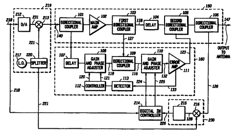
Referring to FIG. 1, there is shown a feed forward amplifier circuit
100 in block diagram form. An analog composite signal 140, which may
include more than one RF carrier, is routed by a directional coupler 101,
causing analog composite signal 140 to be directed to two signal paths.
The two signal paths, an amplifier signal path 150 and a feed forward
signal path 160, generally comprise well known components of a feed
forward amplifier. In amplifier signal path 150, analog composite signal
140 is amplified in a main amplifier 102 and directed to main amplifier
path output as an amplified analog composite signal 147 through a
directional coupler 103, a delay 104, and directional couplers 105 and
106. As previously mentioned, the non-linearity of main amplifier 102
may result in distortion and intermodulation, or error components being
introduced into the signal appearing at the input of directional coupler
103 Accordingly, an amplified analog signal 1 i 8 appearing at the output
of directional coupler 103 will be characterized by carrier components
and error components. The distortion generated by main amplifier 102 is
3 0 the source of these error components which are subsequently canceled
by the feed forward signal path using an output from the feed forward
signal path 160.
The other signal path, feed forward signal path 160, functions to
recreate the error components introduced by amplifier signal path 150. In
3 5 this effort, a sample of analog composite signal 140 .coupled off by
CA 02314108 2000-06-14
WO 99/33167 PCT/US98/16657
directional coupler 101 is delayed in a delay circuit 107, then gain and
phase adjusted in a first gain and phase adjuster 108 without
appreciable distortion being introduced. The time delay of a delay circuit
107 is set to compensate for the signal delay introduced by main
amplifier 102 and directional coupler i 03.
At the output of main amplifier 102, a sample of the distorted
amplified analog signal herein referred to as amplified analog signal
sample 127 {having an error component) is coupled down to directional
coupler 109 via directional coupler 103 where it is recombined 180
degrees out of phase with a feed forvvard signal 119. If the amplitude and
the phase of feed forward signal 119 is properly adjusted by first gain and
phase adjuster 108, the carrier components of amplified analog signal
sample 127 will cancel the carrier components of feed forward signal
119, thereby isolating the distortion. The resulting signal, generally
designated as an error signal 116 will be characterized by error
components. Accordingly, error signal 116 appearing at the output of
directional coupler 109 is representative of the distortion and
intermodulation components introduced by main amplifier 102. This
process is often referred to as carrier cancellation.
Thereafter, the amplitude and phase of error signal 116 is modified
by a second gain and phase adjuster 110, amplified in an error amplifier
111, resulting in an amplified error signal 123. In addition, error amplifier
111 produces a error signal sample 133 suitable for receipt by a detector
113 (discussed below). Amplified error signal 123 is routed to a
directional coupler 105 where it is subtracted from amplified analog
signal 118 via directional coupler 105 and delay circuit 104. The time
delay of delay circuit 104 is set to compensate for the signal delay
introduced by directional coupler 109, second phase and gain adjuster
110, and error amplifier 111. If the amplitude and the phase of error
3 0 signal 1 i 6 is properly adjusted by second gain and phase adjuster 110,
the error components of the main signal path will be canceled, resulting
in a "clean" amplified analog composite signal 147 appearing at the main
amplifier path output.
In order to achieve maximum error component removal, first gain
3 5 and phase adjuster 108 must be controlled to produce a clean error
CA 02314108 2000-06-14
WO 99/33167 PC'TNS98/16657
_g_
signal 116, i.e. one that is substantially representative of the distortion
created by main amplifier 102. A feedback circuit employing error
amplifier 111, detector 113, controller 112 and first phase and gain
adjuster 108 is utilized to reduce the carrier-to-distortion ratio of error
signal 116. The feedback circuit monitors the performance of the carrier
cancellation and then provides dynamic adjustment via controller 112 to
first phase and gain adjuster 108 in order to substantially assure that
error signal 116 is representative of the error components introduced by
main amplifier 102.
During operation, error signal sample 133 is detected by detector
113. Detector 113 may be a DC current detector that detects DC current
drawn by error amplifier 111. The current drawn by error amplifier 111 is
a function of the amount of radio frequency (RF) energy entering the error
amplifier 111 and is proportional to the total carrier energy within the
error signal's passband. The greater the RF energy entering error
amplifier 111, the larger the amount of current drawn by that amplifier
during operation. When the detected DC current indicates sufficient
carrier energy within error signal sample 133, detector 113 provides an
indication to controller 112. In response to the indication, controller 1 i 2
modifies the amplitude and phase parameters of gain and phase adjuster
108 via control lines 120 and 121, thereby adjusting the amplitude and
phase of signals in the feed forward signal path to improve carrier
cancellation at the output of directional coupler 109. Similarly, detector
113 may be implemented as an RF voltage detector that detects levels of
RF voltage sampled from the input or output of error amplifier 111.
An intermodulation cancellation circuit employing error amplifier
111, directional couplers 105 and 106, an IM controller 114, and second
gain and phase adjuster 110 is also utilized to provide maximum
distortion cancellation by monitoring the intermodulation performance of
the feed forward circuit. The intermodulation circuit also provides
dynamic control of second gain and phase adjuster 110 via control lines
124 and 125 in response thereto.
During operation, the amplitude and phase of error signal 116 is
modified by second gain and phase adjuster 110, amplified by error
3 5 amplifier 111, and routed to directional coupler 105 where it is
subtracted
CA 02314108 2000-06-14
WO 99/33167 PCT/US98/16657
_g_
from amplified analog signal 118 via directional coupler 105, in order to
remove error components from amplified analog composite signal 147.
To assure maximum distortion cancellation, a sample of amplified analog
composite signal 147 herein designated as amplified analog composite
signal sample 126 is coupled down from directional coupler 106 and
routed to IM controller 114. In addition, a portion of analog composite
signal 140 is delayed by a delay circuit 115, and then routed to IM
controller 114. If the amplitude and phase of error signal 116 is properly
adjusted, IM controller 114 will detect no distortion in amplified analog
composite signal sample 126. If amplified analog composite signal
sample 126 has error components of sufficient energy, however, IM
controller 114 will modify the amplitude and phase parameters of second
gain and phase adjuster 110, via control lines 124 and 125, thereby
adjusting the amplitude and phase of amplified error signal i23 to drive
the distortion of amplified analog composite signal sample 126 to a
minimum.
As described, feed forward amplifier circuit 100 provides
improvement in the phase and gain adjustment of an error signal in a
feed forward signal path. Although the improvement is substantial, it
does not fully address cancellation of possible residual carrier
components appearing at the input of IM controller 114. The possible
residual carrier components resulting from the distorted frequency
response of main amplifier 102 may intertere with the ability of IM
controller 114 to accurately detect residual error components. The
compromised ability of IM controller 114 to detect residual error
components may then result in a degradation of control to phase and
gain adjustments of the error signal in a feed forward signal path.
Referring to FIG. 2, there is shown in a block diagram, a preferred
embodiment of the feed forward amplifier circuit, according to the present
invention. Similar to the feed forward amplifier depicted in FIG. 1, the
preferred embodiment of the feed forward amplifier circuit includes
amplifier signal path 150 and feed forward signal path 160. Whenever
possible, like components in each path are made from the same material,
3 5 and preferably on the same board in a single board amplifier.
CA 02314108 2000-06-14
WO 99/33167 PCTNS98/16657
-10-
As is evident, FIG. 2 additionally comprises an up-converter 219,
and a down-converter 230. Further, a digital signal appearing at the
input of up-converter 219 provides a first digital input 218 to IM controller
214. First digital input 218 is representative of a plurality of summed
ideal digital signals which are to be subsequently shifted via up-converter
219 to a higher frequency, amplified and combined with the output from
feed forward signal path 160, and transmitted at the main amplifier path
output. In the preferred embodiment, first digital input 218 is provided by
a transmitter combiner card (not shown), but may be provided by any
suitable source. As is also evident, upon receiving an amplified analog
composite signal sample 126 from directional coupler 106, down-
converter 230 provides a second digital input 226 to IM controller 214.
Down-converter 230 includes an analog-to-digital converter 215 and a
first mixer 216. First mixer 216 operates to down-shift the frequency of
amplified analog composite signal sample 126 to produce an adjusted
composite analog signal sample 128 such that its frequency is suitable
for input to digital IM controller 214. Further, analog-to-digital converter
215 converts adjusted composite analog signal sample 128 to a small
amplitude digital signal stream appearing as second digital input 226 to
digital IM controller 214. Second digital input 226 is representative of a
plurality of summed real digital signals resulting from a low power sample
of amplified analog composite signal 147 appearing at the main amplifier
path output.
Additionally, first digital input 218 is converted to an analog signal
2 5 and frequency shifted by up-converter 219. Up-converter 219 includes a
digital-to-analog converter 212 which converts first digital input 218 to an
analog signal 231, a second mixer 213, a splitter 220, and a local
oscillator 217. Local oscillator 217 generates a reference frequency
signal 221, which when mixed via second mixer 213 with analog signal
3 0 231, produces an analog composite input signal 140 suitable for receipt
by main amplifier 102. In addition to providing reference frequency
signal 221 to second mixer 213, splitter 220 provides reference
frequency signal 221 to first mixer 216. This ensures that second digital
input 226 is at the same frequency as first digital input 218 as is required
3 5 for proper functioning of digital IM controller 214.
CA 02314108 2000-06-14
WO 99/33167 PCf/US98/16657
-11-
As discussed in connection with FIG. 2., first digital input 218
represents a plurality of summed ideal digital signals which have not
been amplified by main amplifier 102 and therefore are "ideal" in that it
only comprises carrier components. Conversely, second digital input 226
represents a plurality of digital signals which have been converted to an
analog signal and amplified by main amplifier 102, resulting in the
addition of error components. Theoretically, all of the error components
are then removed as a consequence of feed forward amplifier operation.
and a clean distortionless {i.e. no error components), amplified output
signal is produced. Although the majority of the error components are
removed, in reality, a "real" analog signal including carrier components
and residual error components is produced at the output of directional
coupler 105. According to a preferred embodiment of the present
invention, reduction of residual error components is accomplished in the
digital domain through the use of a digitally enabled IM controller such as
digital IM controller 214. The resulting gain and phase manipulation of
error signal 116 via a gain adjuster input 224 and a phase adjuster input
225 to second gain and phase adjuster 110 is accomplished as a result
of a measure of the difference between first digital signal 218 and second
digital signal 226 by digital IM controller 214 (discussed below).
Digital IM controller 214 is constructed as shown in FIG. 3. Digital
IM controller 214 includes an adaptive finite impulse response (FIR) filter
310 for receiving first digital input 218, a carrier cancellation controller
308, a subtractor 306, a total power detector 304 and an IM cancellation
controller 302 for providing gain and phase adjuster inputs (224, 225) to
second gain and phase adjuster 110.
Adaptive FIR filter 310 operates to align first digital input 218 with
second digital input 226, the operation and construction of adaptive filters
3 0 being well known in the art. The alignment is accomplished via delaying
and then adjusting the amplitude and frequency response of first digital
signal 218 based on multiple tap inputs 315 (discussed below) received
from carrier cancellation controller 308. A resulting aligned first digital
signal 311 from adaptive FIR filter 310 is subtracted from second digital
3 5 input 226 in subtractor 306, yielding a subtractor output 313.
CA 02314108 2000-06-14
WO 99/33167 PCT/US98/16657
- -12-
As was previously mentioned, aligned first digital input 311 results
from a plurality of digital signals which include carrier components while
second digital input 226 represents a plurality of digital signals which
include both carrier components and residual error components.
S Accordingly; subtractor 306 provides subtractor output 313 representative
of residual error components as well as possible residual carrier
components.
Carrier cancellation controller 308 operates to provide
adjustments to adaptive FIR filter 310 through the use of multiple tap
inputs 315. Carrier cancellation controller 308 receives two inputs, first
digital input 218 and subtractor output 313. Adjustments via multiple tap
inputs 315 to adaptive F1R filter 310 are accomplished by correlating first
digital input 218 with subtractor output 313. Carrier cancellation circuit
308 then adjusts multiple tap inputs 315 so as to minimize this correlation
at each of the delay values associated with the taps in adaptive filter 310.
This iterative feedback technique removes subsequent residual carrier
components appearing in subtractor output 313 as aligned first digital
input 311 and second digital signal 226 become substantially identical in
frequency response gain, phase and delay. In addition, carrier
cancellation circuit 308, upon noting that correlation calculations used to
adjust multiple tap inputs 315 yield values that are below some
predetermined threshold, provides an indicator signal 321 to IM
cancellation controller. 302 (discussed below). Carrier cancellation
controller 308 may be implemented via a digital signal processor or
2 5 custom integrated circuit.
In addition to providing input to carrier cancellation controller 308,
subtractor output 313 provides input to total power detector 304.
Subtractor output 313 appears at the input of total power detector 304 as
a digital distortion signal representative of the residual error components
present in second digital input 226. Total power detector 304 is a digital
detection envelope function provided by a multiplier to multiply subtractor
output 313 by its complex conjugate, and a low pass digital filter. Total
power detector 304 provides an averaging function, which yields a digital
value 316, representative of the power of the residual error components
3 5 present in second digital input 226. Digital value 316 may be formed
CA 02314108 2000-06-14
WO 99/33167 PCTNS98/16657
-13-
using a number of methods. Such methods may include summing a
predefined number of subtractor outputs 313, or replacing the oldest
previous subtractor output on a stack of buffered outputs with the current
subtractor output and then summing the buffered outputs. Next, digital
value 316 is compared with a previous digital value previously generated
by total power detector 304 by IM cancellation controller 302, thus
forming a comparison value. Based on the comparison value, gain
adjuster input 224 and phase adjuster input 225 are modified.
IM cancellation controller 302 remains idle until it receives an
indicator signal 321 from the carrier cancellation controller 308 indicating
that the carrier cancellation process in carrier cancellation controller 308,
has converged. Carrier cancellation controller 308 is said to have
converged when all the correlation calculations used to adjust multiple
tap inputs 315 yield values that are below a predetermined threshold.
Utilization of indicator signal 321 prevents IM cancellation controller 302
from making improper adjustments during start up, during which time the
output of total power detector 304 is varying dramatically due to the
action of carrier cancellation controller 308.
IM cancellation controller 302 operates as follows. Upon receipt of
a suitable indicator signal 321 from carrier cancellation controller 308, IM
cancellation controller 302 begins its IM cancellation process. First,
digital value 316 is measured after waiting for a period of time at least
equal to the averaging interval used in total power detector 304. A small
change, dV, is then temporarily made to gain adjuster input 224. After
again waiting for the averaging process in total power detector 304 to
complete, digital value 316 is re-measured, forming a new level. If this
new level is significantly lower than the previous level, then gain adjuster
input 224 is changed by Q*dV, where Q is some number between 0 and
1. If this new level is significantly higher than the previous level, then
gain
3 0 adjuster input 224 is changed by -Q*dV. If this new level is not
significantly different from the previous level, then gain adjuster input 224
is not changed. The IM cancellation process is then repeated using
phase adjuster input 225 instead of gain adjuster input 224. The entire
cycle of adjusting gain adjuster input 224 and phase adjuster input 225 to
3 5 second gain and phase adjuster 110 is then repeated continuously. The
CA 02314108 2000-06-14
WO 99/33167 PCT/US98/16657
-14-
adjusting subsequently affects amplified analog composite signal sample
126 and therefor second digital input 226.
FIG. 4 is a flow chart illustrating those steps necessary for
generating a phase adjuster input and a gain adjuster input 224, 225 to a
feed forward amplifier 100 by digital IM controller 214 of FIG. 3 in
accordance with the preferred embodiment of the present invention. The
logic flow starts at step 42 where adaptive F1R filter 310 receives first
digital input 218 which is comprised of a plurality of summed ideal digital
signals. Adaptive FIR filter 310 then adjusts the amplitude and frequency
response of first digital input 218 in response to a plurality of multiple tap
inputs 315 and forms aligned first digital signal 311, at step 44. Next at
step 46, subtractor 306 receives aligned first digital signal 311 and
second digital input 226. Second digital input 226 is comprised of a
Z 5 plurality of summed real digital signals including error components.
Subtractor 306 subtracts aligned first digital signal 311 from second
digital input 226, yielding a subtractor output 313, at step 48. Subtractor
output 313 is comprised of residual error components and possible
residual carrier components. Next, at step 50, carrier cancellation
controller 308 correlates first digital input 2i8 with subtractor output 313,
generating indicator signal 321 for receipt by intermodulation
cancellation controller 302. In addition, the results of the correlation
provide an adjustment to multiple tap inputs 315. Subtractor output 313
also provides the input to total power detector 304 which converts the
power of the subtractor output 313 into digital value 316, at step 52. Next,
at block 54, digital value 316 is received by intermodulation cancellation
controller 302 which then compares digital value 316 to the previous
digital value generated by total power detector 304. The comparison
yields a comparison value. At step 56, in response to the comparison
3 0 value, intermodulation cancellation controller 302 generates gain
adjuster input 224 and phase adjuster input 225 for receipt by feed
forward amplifier 100. Finally at step 58, the previous digital value used
in step 54 is replaced by digital value 316 and the flow passes back to
step 52. Subsequently, a new digital value is generated, replacing digital
3 5 value 316. Steps 52, 54, and 56 are repeated continuously in order to
CA 02314108 2000-06-14
WO 99/33167 PCTNS98/16657
-15-
keep gain adjuster input 224 and phase adjuster input 225 set at the
levels required to minimize the error components in amplified analog
composite signal 147.
While the invention has been particularly shown and described
with reference to a particular embodiment, it will be understood by those
skilled in the art that various changes in form and details may be made
therein without departing from the spirit and scope of the invention.