Note: Descriptions are shown in the official language in which they were submitted.
CA 02314125 2000-06-12
WO 99/30272 PCT/US98/26448
TOUCH SENSITIVE SCREEN AND ITS MANUFACTURING METHOD
FIELD OF THE INVENTION
The present invention relates to devices for sensing the X-Y coordinates of a
touch
on a surface thereof. The present invention more particularly provides a
resistive touch-
screen whereby touch coordinates can be determined with excellent linearity
throughout an
increased proportion of its touch-sensitive area. The present invention also
provides a
method for producing a touchscreen having reduced bow, or reduced variation of
bow, of
equipotential field lines therein.
BACKGROUND OF THE INVENTION
A touchscreen is an input device, placed over a display such as a cathode ray
tube
(CRT) or a liquid crystal display, for sensing the two-dimensional position of
the touch of a
fmger or other electronically passive stylus. Such systems are provided for
many appli-
cations including restaurant order entry systems, industrial process
controllers, interactive
museum exhibits, public information kiosks, lap-top computers, etc. Many
schemes have
been proposed for touchscreen construction. Presently, the commercially
dominant touch
technologies are 4-wire resistive, 5-wire resistive, capacitive, and
ultrasonic.
5-Wire resistive touchscreens, e.g. the AccuTouchTM product line of Elo Touch-
Systems, Inc., of Fremont, California, are widely accepted for many
touchscreen applica-
tions. Mechanical pressure from a finger or stylus causes a plastic membrane
coversheet to
flex and make physical contact with an underlying glass substrate, coated with
a resistive
layer upon which voltage gradients are excited. Via electrical connections to
the four cor-
ners of the glass substrate, associated electronics can sequentially excite
gradients in both
the X and Y directions. The underside of the coversheet has a conductive
coating which
provides an electrical connection between the touch location and voltage
sensing elec-
tronics. There are a total of five electrical connections, i.e., "5 wires",
between the touch-
screen and the controller electronics. Further details regarding 5-wire
touchscreens are
found in the US 4,220,815; 4,661,655; 4,731,508; 4,822,957; 5,045,644; and
5,220,136.
-1-
CA 02314125 2000-06-12
WO 99/30272 PCT/US98/26448
4-Wire resistive touchscreens have lower manufacturing costs than 5-wire ones
and
dominate the low-end market. However, in applications demanding durability,
the 5-wire
technology is superior. To measure X and Y coordinates, 4-wire touchscreens
alternate
between exciting a voltage gradient on the substrate resistive coating and
exciting an
orthogonal voltage gradient on the coversheet coating. Performance of 4-wire
touchscreens
degrades as the uniform resistivity of the coversheet coating is lost as a
result of repeated
flexing. This is not a problem for 5-wire touchscreens where both X and Y
voltage gra-
dients are generated on the substrate's resistive coating, and the coversheet
coating need
only provide electrical continuity. However, in a 5-wire touchscreen, a
peripheral electrode
pattern of some complexity is required to enable sequential generation of both
X and Y
voltage gradients on the same resistive coating. This is a major reason why 5-
wire
touchscreens are costlier to manufacture than 4-wire ones.
In a 5-wire touchscreen the substrate typically comprises about 1.0 mm to
about 3.0
mm thick glass, on which has been applied the resistive coating, typically
indium tin oxide
(ITO), as well as a peripheral electrode pattern. The peripheral electrode
pattern forms a
resistor network which is powered at the four corners by excitation voltages
from controller
electronics. In turn, the electrode pattern excites voltage gradients in the
ITO corres-
ponding to the touchscreen active area. A key issue is minimization the cost
of this coated
and patterned substrate component.
Conductive traces connect the four corners of the electrode pattern to a group
of
soldering pads where a simple five-wire ribbon cable is connected. This
reduces the cost of
the fully assembled touchscreen by eliminating the need for a complex cable
harness and
wire routing. A screen-printed silver frit is the typical material for these
traces due to its
high conductivity, durability, and its ability to accept solder connections.
The silver-frit
traces are isolated by nearby insulating regions of bare glass substrate.
Hence the glass
substrate has three components: conductive regions upon which silver frit has
been sintered,
insulating regions of bare glass, and resistive regions coated with ITO.
Commercially, the peripheral electrode pattern may be created via geometrical
arrangements of the aforementioned three ingredients. To control costs, the
resistive ITO
coating in the peripheral electrode region is created in the same
manufacturing step and
-2-
CA 02314125 2000-06-12
WO 99/30272 PCT/US98/26448
with the same nominal electronic characteristics as in the region in where X
and Y voltage
gradients are generated. An example is the electrode design given in Figure 1C
herein,
reproduced from US 5,045,644. Such electrode designs that only use the above
mentioned
materials play a key role in state-of-the-art 5-wire touchscreen technology.
A quality 5-wire touchscreen will generate X,Y coordinates that accurately
corres-
pond to the touch position. Accuracy is largely determined by the "linearity"
of the touch-
screen. In the ITO coating within the touch region of an ideally linear
touchscreen, the
contours of equal voltage, i.e. equipotential lines, are equally spaced
straight lines ortho-
gonal to the X or Y coordinate being measured. Deviations from linearity occur
in practice.
The design of the peripheral electrode pattern may not be fully optimized.
Also, manufac-
turing variations in the uniformity of the ITO coating cause deviations from
ideal linearity.
A central problem for 5-wire resistive technology is to find the most cost-
effective way to
achieve sufficient linearity to meet marketplace demands.
One approach is to insist on tight manufacturing tolerances for the uniformity
of the
resistivity of the ITO coating. This assures quality product performance but
has the
disadvantage of driving up the cost of the ITO coating process.
Another approach is to design the peripheral electrode patterns to be more
tolerant
to variations in ITO resistivity. This approach generally leads to increased
current draw
through the electrode pattern. This is undesirable in many applications as it
places greater
power demands on the associated controller electronics. This approach may also
lead to an
increased width of the peripheral electrode pattern.
BRIEF SUMMARY OF THE INVENTION
Therefore, what is needed and what has been invented is an electrographic
touch
sensor and method which compensate for batch-to-batch variations in the
resistive layer and
for the limitations of the in-place electrodes - in particular, a resistive
touch sensor and
method for controlling the flow of current through a resistive layer for
converting physical
position information on the resistive layer into electrical signals by
modifying the resistance
characteristics of the resistive layer.
-3-
CA 02314125 2000-06-12
WO 99/30272 PCTIUS98/26448
The present invention accomplishes its desired objects by broadly providing a
position touch sensor comprising a resistive surface (i.e., an impedance
surface) having
resistive perimeter edges; and at least one pair of electrodes disposed on,
and electrically
connected to, the resistive surface. The position touch sensor further
includes at least one
pair of spaced electrode segments to provide generally opposed boundaries for
defining an
overlapped resistive region between the spaced electrode segments. The
resistive surface
has at least one insulating region (e.g., a void, an insulating segment or
channel, etc.)
commencing from a resistive point in the resistive surface exterior to the
overlapped
resistive region and terminating in the overlapped resistive region.
The present invention further accomplishes its desired objects by also broadly
providing a method of modifying the resistance characteristics of a resistive
layer between a
pair of parallel electrode segments of a position touch sensor comprising the
steps of:
a) providing a position touch sensor comprising a substrate having adherently
deposited thereon a resistive layer having a resistive portion, and at least
one pair of
generally parallel spaced electrode segments positioned on, and electrically
connected to,
the resistive layer and including an overlapped resistive region between the
generally
parallel spaced electrode segments and integrally contained within the
resistive layer such
that the overlapped resistive region includes the resistive portion with the
overlapped
resistive region indiscreetly merging with an external resistive region
outside of the
overlapped resistive region and integrally contained within the resistive
layer such that the
external resistive region includes the resistive portion; and
b) altering the resistive portion of the overlapped resistive region and of
the
external resistive region.
The present invention also further accomplishes its desired objects by also
further
broadly providing a method for controlling the flow of current through a
resistive layer for
converting physical position information on the resistive layer into
electrical signals
comprising the steps of:
a) providing a resistive layer for converting physical position information
thereon into electrical signals;
-4-
CA 02314125 2000-06-12
WO 99/30272 PCTIUS98/26448
b) determining through the use of electrical excitation in the resistive layer
a
dimension of a length of a generally continuous resistive section which is to
be located in
the resistive layer of step (a);
c) disposing a first insulating region in the resistive layer of step (a) to
form a
first boundary of the generally continuous resistive section; and
d) disposing, at a distance from the first insulating region essentially
equaling
the dimension of step (b), a second insulating region in the resistive layer
of step (a) to form
a second boundary of the generally continuous resistive section such that
current may be
conducted through the generally continuous resistive section between the first
insulating
region and the second insulating region.
BRIEF DESCRIPTION OF THE DRAWING(S)
Figs. lA and 1B are drawing illustrating, respectively, a "ruler line plot"
and the
equipotential lines as obtained using the gradient sheet of a conventional
touchscreen;
Fig. 1 C is a top elevational view of another conventional gradient sheet
having
plural overlapping conductive strips communicating with plural T-shaped
electrodes;
Fig. 2A is a top elevational view of another conventional gradient sheet
having a
resistive element/electrode configuration to reduce bow equipotential field
lines therein;
FIG. 2B is a partial top elevational view which illustrates the spacing of the
resistance elements/electrodes shown in Fig. 2A;
Fig. 3 is a schematic diagram of a resistive touchscreen system, while Fig. 4
is a
perspective view of a CRT incorporating the resistive touchscreen system of
Fig. 3;
Fig. 5 is a segmented perspective view of the touchscreen of Fig. 3
incorporating the
present invention;
Fig. 6 is a top plan view of a portion of a gradient sheet having a resistor
chain
comprising overlapping conductive strips with a conductive lead coupling a T-
shaped
electrode to one of the conductive strips and including an insulating region
having an
insulating region portion extending into and terminating in an overlapped
resistive region
between the overlapping conductive strips and communicating with another
insulating
region portion which extends outside of the overlapped resistive region;
-5-
CA 02314125 2000-06-12
WO 99/30272 PCT/US98/26448
Fig. 6A is a top plan view of another embodiment of the Fig. 6 gradient sheet;
Fig. 6B is a partial vertical sectional view of a gradient sheet including a
substrate
supporting a semiconductive resistive layer which has been altered by the
formation of a
channel therein to provide an insulating zone in the semiconductive resistive
layer;
Fig. 6C is a partial vertical sectional view of a gradient sheet including a
substrate
supporting a semiconductive resistive layer altered by the formation of
another channel
therein to provide another insulating zone in the semiconductive resistive
layer;
Fig. 7 is a top plan view of a portion of a gradient sheet having a resistor
chain com-
prising a plurality of conductive strips serially disposed in proximity to an
edge of the
gradient sheet with any two contiguous conductive strips spaced by an
overlapped resistive
region and having a pair of opposed insulating region portions extending into
and termi-
nating in the overlapped resistive region with the pair of opposed insulation
region portions
each communicating with an insulating region outside of the overlapped
resistive region;
Fig. 8 is a top plan view of a portion of a gradient sheet having a resistor
chain
comprising overlapping conductive strips having an overlapped resistive region
between
conductive strips and including T-shaped insulating regions partly disposed
outside of the
overlapped resistive region and partly extending into and terminating in the
overlapped
resistive region with the portion of the T-shaped insulating region extending
into the
overlapped resistive region having an insulating subsection which is generally
parallel to
the overlapping conductive strips;
Fig. 9 is a top plan view of another embodiment of the Fig. 8 gradient sheet
but with
the insulating subsection communicating with another insulating subsection
which is
generally normal thereto and terminating in and contacting two contiguous
opposed
overlapping conductive strips within the overlapped resistive region and with
the portion of
the T-shaped insulating region disposed outside of the overlapped resistive
region
terminating in and making contact with the same two opposed contiguous
overlapping
conductive strips outside of the overlapped resistive region;
Fig. 10 is a top plan view of another embodiment of the Fig. 9 gradient sheet
with
the other insulating subsection overlapping the two opposed contiguous
overlapping
conductive strips within the overlapped resistive region and with the T-shaped
insulating
-6-
CA 02314125 2000-06-12
WO 99/30272 PCT/US98/26448
region disposed outside of the overlapped resistive region overlapping the two
opposed
contiguous overlapping conductive strips at an angle thereto;
Fig. 11 is a top plan view of a gradient sheet having the resistor chain and
insulating
region of Fig. 9 thereon; and
Fig. 12 is a schematic side elevational view of a capacitive toouchscreen
embodiment of the present invention having a substrate covered by a resistive
layer upon
which are a plurality of conductive electrodes, in turn are covered by a
dielectric layer, with
a portion of the resistive layer having been removed to form an insulating
zone.
DETAILED DESCRIPTION OF THE INVENTION
Referring in detail now to the drawings wherein similar parts of the present
invention are identified by like reference numerals, there is seen in Figs. 1
A-2B various
prior art gradient sheets which are intended to reduce the curvature (i.e.,
"bow") produced
by the voltage drop along a resistor network attached to resistive electrodes
in a direction
perpendicular to the applied voltages. The performance of any touch sensitive
screen can
be demonstrated with what is known as a "ruler line plot," which is what a
rectangular set
of lines would look like if impressed upon the sensor, and an "equipotential
line plot"
showing the location of equal potentials on the sensor. For example and as
best described
in US 5,045,644, Fig. lA shows a ruler line plot 50 on a gradient sheet 52 of
the sensor,
while Fig. 1B shows an equipotential line plot 55 on gradient sheet 52. These
line plots
shown, typically, represent each 0.1 volt differences. There is substantial
ripple 60 along
edges 65 of gradient sheet 52, and particularly near corner 67. Ruler line
plot 50 only has
straight lines 70 at a significant distance from edges 65. The area of
straight lines 70
defines the linear portion of gradient sheet 52.
US 5,045,644 also discloses another prior art gradient sheet, represented in
Fig. 1 C
as a gradient sheet 195' having a central uniform resistive layer 205 of, for
example, two
hundred ohms per square. Positioned along each edge of the surface of gradient
sheet 195'
is a resistor chain 245', formed of a series of overlapping conductive strips
350. Using
these overlapping conductive strips 350 and the resistivity of resistive layer
205, the spe-
cific resistances of resistor chain 245' can be tailored for a particular
application and distri-
-7-
CA 02314125 2000-06-12
WO 99/30272 PCT/US98/26448
bution of voltages along the edges of gradient sheet 195. Conductive strips
350 are physi-
cally attached to resistive surface 205 by depositing a conductive material,
e.g., silver frit,
in the appropriate pattern. A conductive corner tab 355 applies a voltage to
the end of
resistor chain 245', and a conductive lead 360 typically connects conductive
corner tab 355
to a tab (not shown) at another location of gradient sheet 195'. This
connection between
the conductive corner tabs can be external to gradient sheet 195'. Conductive
corner tab 355
is connected to appropriate external circuitry for supplying the voltage
source.
US 5,045,644 further discloses a plurality of T-shaped electrodes (or "tees")
365
spaced along the edges of resistive layer 205. A conductive lead 370 connects
a T-shaped
electrode 365 to resistor chain 245'. The position of conductive leads 370
along resistor
chains 245' is selected to provide the appropriate reference voltage to T-
shaped electrodes
365. The length and spacing of T-shaped electrodes 365 are chosen to
compensate for any
cumulative voltage drop along resistor chain 245' portion which is
perpendicular to the
current flow on resistive layer 205. Elongated regions 300 of high resistance,
produced by
no deposit of resistive layer 205 on gradient sheet 195', are aligned with and
interspersed
between the bases of T-shaped electrodes 365. This substantially isolates the
main portion
of resistive layer 205 from that portion 205a in the region of resistor chains
245'. The
spacings and effective lengths of T-shaped electrodes 365 are selected to
produce a voltage
gradient at each T-shaped electrode 365 to compensate for any voltage drop
which occurs
along resistor chain 245'.
Referring now to Figs. 2A and 2B, which illustrate a prior art gradient sheet
from
US 4,822,957, there are seen conductive electrodes 85 positioned along the
edges of a
resistive layer 84 of gradient sheet 86. Additional conductive electrodes 88
are positioned
along each edge, with each electrode 88 being joined to an adjacent conductive
electrode 85
by a conductive connector or lead 90. The spacing and effective lengths of
electrodes 88
are selected to produce a voltage gradient at each electrode 88 to compensate
for any volt-
age drop that occurs along the resistance elements between conductive
electrodes 85. A
pair of overlapping conductive legs 92, 94 overlap a length L' and are spaced
apart a
distance D (Fig. 2B). The resistance produced at each overlap between
conductive elec-
trodes 85 is a function of D, L', and the resistivity of resistive layer 84.
The patent teaches
-8-
CA 02314125 2000-06-12
WO 99/30272 PCT/US98/26448
that the location of the connection between conductive electrode 85 and
electrode lead 90 is
not critical, as long as the resistance of each conductive electrode 85 is
sufficiently low.
Fine tuning of the resistance of each overlap between conductive electrodes 85
can be
achieved by shortening or lengthening one or both of conductive legs 92, 94 to
change L'.
This can be accomplished readily by changing the artwork used for screen
printing tech-
niques. To prevent undesirable current flow between conductive electrodes 85
and con-
ductive electrodes 88, a line 87 of discontinuity is formed between conductive
electrodes 85
and 88. Line 87 is where there is no resistive layer 84 and represents a
discontinuity in
resistive layer 84. Line 87 produces a central resistive area 84A and a
peripheral resistive
area 84B, and is taught as being formed by either not depositing any resistive
layer 84 along
line 87 or removing portions of resistive layer 84 after application. In
either case conduc-
tive connectors 90 span or bridge line 87 so as to connect conductive
electrodes 88 to con-
ductive electrodes 85. Line 87 is placed on gradient sheet 86 before the
placement of
conductive electrodes 85 and conductive electrode 88 on resistive layer 84 and
does not
serve to determine the resistance value of the overlapped region between
overlapping
conductive legs 92 and 94 of conductive electrodes 85, but rather serves to
isolate this
overlapped region from central resistive area 84A.
Referring in detail now to Figs. 3-12 of the drawings for preferred
embodiments of
the present invention, in Fig. 3 there is seen a generalized system diagram of
a resistive
touchscreen system 100. Resistive touchscreen system 100 includes a
touchscreen 105
coupled via controller electronics 110 to a host computer 115. Generally,
controller
electronics 110 receives from touchscreen 105 analog signals carrying touch
information.
Controller electronics 110 also sends to touchscreen 105 excitation signals.
Specifically,
controller electronics 110 applies a voltage gradient across a resistive layer
205 (see Fig. 5)
which is disposed on a substrate 200 of touchscreen 105. The voltages at the
point of
contact are the analog representations of the position touched. Controller
electronics 110
digitizes these voltages and transmits these digitized signals, or touch
infonnation in digital
form based on these digitized signals, to host computer 115 for processing.
As best shown in Fig. 4, touchscreen 105 may be installed in a conventional
display
device such as a CRT 145. Touchscreen 105 is placed in front of CRT face 150
of host
-9-
CA 02314125 2000-06-12
WO 99/30272 PCTIUS98/26448
computer 115 and under CRT monitor bezel 155. A plurality of spacers 111 is
con-
veniently provided in order to create a gap for touchscreen 105 between CRT
monitor bezel
155 and CRT face 150. A high voltage anode 117 (not fiilly shown in Fig. 4) is
coupled to
a CRT circuit board 113 via an electrical cable 139. A touchscreen ribbon
cable 131 con-
nects from touchscreen 105 to an outlet 133 which is to receive electrical
power and which
is to interfaces with controller 110 (not shown). A ground strap 129 connects
from a chas-
sis ground 147 to outlet 133. Display device 145, along with CRT circuit board
113 and
associated cables, are all received by a generally hollow monitor back case,
illustrated as
121. Preferably, the components of touchscreen 105 are substantially
transparent so that
the two dimensional graphics or data projected by CRT face 150 is seen
theret.hrough.
Alternatively, resistive touchscreen system 100 may be installed in other
suitable
types of display devices, such as a liquid crystal display monitor.
Controller electronics 110 may be a separate electronics module, such as Elo
Model
E271-140 AccuTouchTM controller, from Elo TouchSystems or may be largely
embedded
in host computer 115, such as the digitizer panel interface contained in
central processing
unit (CPU) chip of a handheld computer system based on Intel 1386TM EX
Embedded
Microprocessor MHT9000 Handheld Terminal. Other controller options are also
possible.
Controller electronics 110 may perform various functions. For example, it may
excite the electrode pattern and measure the voltage on cover sheet 210 (see
Fig. 5 ) of
touch screen 105. This function is performed by the aforementioned Elo Model
E271-140
AccuTouchTM controller. Alternatively, controller electronics 110 may connect
cover
sheet 210 to a current source, ground the four corners of the electrode
pattern on cover sheet
210,-and digitize the currents for the electrode-pattern corners. As another
option, control-
ler electronics 110 may support AC operation of the invention by driving the
four electrode-
pattern corners with an AC signal having a fixed voltage amplitude, replacing
coversheet
210 with a thin dielectric coating 725 (Fig. 12) applied directly to resistive
layer 205, and
by then detecting changes in the corner currents resulting from the AC current
sinking from
a finger (or stylus) contact on the sensor. Controller electronics 110
performing these AC
functions are also known as capacitive touchscreen controllers. The present
invention
-10-
CA 02314125 2005-11-23
improves linearity in other touchscreen systems employing other types of
controller
electronics.
Controller electronics 110 and/or host computer 115 may include algorithms for
correcting non-linearities in the touchscreen sensor according to the present
invention.
Correction of non-linearities may become important if the touchscreen is
designed to
consume low power and/or have narrow borders. For such algorithms, "correction
coefficients" for non-linear corrections are produced and used for
compensating for non-
linearities, e.g., as described in WO 97/34273.
Fig. 5 shows an exploded segmented view of the components of touchscreen 105
in
accordance with one preferred embodiment of the present invention. It will be
recognized
that the thickness, height, or other dimensions of some of the components in
some of the
drawings has been exaggerated for purposes of illustration. Touchscreen 105
comprises a
gradient sheet 195 including a substrate 200 having a uniform resistive layer
205
permanently applied to one surface thereof. Preferably, uniform resistive
layer 205 is
durable (adherent, chemically stable, etc.). Resistive layer 205 further
includes a touch
region which is generally illustrated as 206 in Fig. 5.
The geometry of substrate 200 may be planar (as shown in Fig. 5) or may be
contoured to match the face of a curved object, such as CRT face 150 of Fig.
4. Substrate
200 can also have any perimeter configuration, e.g., substantially rectangular
to match the
configuration of a typical video display. Substrate 200 can also have a
perimeter
configuration which matches the configuration of a circular touch sensor as
described in US
4,777,328. Typically, a substrate 200 constructed from glass will have a
resistivity value in
excess of about 108 ohms per square. This substrate 200 typically has a
thickness of about
two to three millimeters.
For a substantially transparent touch sensor, substrate 200 may be constructed
from
glass, plastic, or from other substantially transparent materials.
Additionally, resistive layer
205 on substrate 200 should also be substantially transparent (i.e.,
transmission of at least
60%, and preferably at least 80%). In such instance, resistive layer 205 is
typically a
semiconducting metal oxide such as ITO.
-11-
CA 02314125 2000-06-12
WO 99/30272 PCTIUS98/26448
Alternatively, if the product is to be an opaque sensor, substrate 200 may be
glass,
acrylic or other rigid plastic, or various types of printed circuit board
materials, or a metal
having a previously applied insulating layer. Furthermore, various plastic
materials for
substrate 200 can be utilized in the form of flexible sheets and supported
upon a suitable
hard surface material. Resistive layer 205 is typically adherently applied by
screening a
resistive ink or by spraying a resistive paint upon substrate 200. Or,
resistive layer 205 may
be a volume of conducting sheet such as rubber or plastic. For an opaque
sensor, resistive
layer 205 may have a sheet resistivity ranging from about 10 to about 10,000
ohms per
square and can be applied within a variation of uniformity of about one
percent to about
twenty-five percent, depending upon the positional accuracy needed.
Typically, resistive layer 205, if it comprises ITO, has an approximately
uniform
resistivity from about 10 to about 10,000 ohms per square, preferably, from
about 100 to
about 1,000 ohms per square, and more preferably from about 150 to about 300
ohms per
square. Typically, its thickness is less than a wavelength of light.
Resistive layer 205 may be other semiconducting metal oxides such as indium
oxide, tantalum oxide, tin oxide, antimony oxide, or a combined layer of,
e.g., antimony
oxide and tin oxide. Other similar resistive layers which are adherent,
chemically stable,
and provide a resistance in the range of from about 100 to about 3,000 ohms
per square,
without excessively reducing the transparency of the sensor, are suitable. In
general,
nonstoichiometric oxides of metals in Groups III and IV, with metal impurities
from
adjoining Groups of the Periodic Table of Elements, are suitable.
Substrates having ITO resistive layers are described in more detail in US
4,220,815.
Such ITO-coated substrates may be purchased commercially, for example, from
Optical
Coating Laboratory, Inc. (OCLI) of Santa Rosa, California, and Information
Products, Inc.
(IPI) of Holland, Michigan.
Continuing to refer to Fig. 5, spaced a small distance above resistive layer
205 is a
cover sheet 210, which is typically a flexible film 215 having a conductive
coating 220 on
its underside. Cover sheet 210 prevents any damage to resistive layer 205.
Typically,
flexible film 215 has a stiff and durable coating possessing a clear or anti-
glare finish. The
thickness of flexible film 215 may be, for example, about 0.005 inch (0.125
rnm). Flexible
-12-
CA 02314125 2000-06-12
WO 99/30272 PCT/US98126448
film 215 may be manufactured from a rigid-like plastic (such as polyester or
poly-
carbonate), polyvinylchloride, or an elastomeric material, or any other
suitable material.
If the sensor is to be transparent, then conductive coating 220 must also be
transparent or substantially so and may be, for example, a deposit of a metal
such as gold-
nickel or a semiconductor such as an oxide of a metal selected from the group
consisting of
tantalum, indium, antimony, and mixtures thereof, with ITO being preferred..
While the embodiment of Fig. 5 utilizes a cover sheet, the present invention
is not
so limited. For example, any conducting element, such as a conducting stylus
(not shown
.in Fig. 5), can be used as an alternative means for contacting resistive
layer 205. This
conducting stylus may be used when resistive layer 205 is sufficiently durable
as to
withstand damage from such contact. As another alternative, a capacitive or
resistive
pickup system can be used along with a user's finger or with an appropriate
probe.
As further shown in Fig. 5, cover sheet 210 is typically joined to the rest of
touch-
screen 105 by an adhesive along its associated edges or, optionally, by an
insulative adhe-
sive frame 225 or the like. Additionally, an electrode 230 connects conductive
coating 220
via lead 235 to an appropriate external circuitry, such as controller circuit
110.
Typically, conductive coating 220 is separated from resistive layer 205 by a
plurality of small transparent insulator islands or dots 240, which prevent
accidental contact
between conductive coating 220 and resistive layer 205, but yet permit contact
there-
between by a small applied pressure from a fmger or of a small object. These
insulator
islands are further shown and described in US 4,220,815 and 5,220,136.
With continuing reference to Fig. 5, a resistor chain 245 is spaced along each
edge
of resistive layer 205 and is used for applying potentials to resistive layer
205 so as to
create orthogonal voltage gradients therein. As shown in subsequent figures,
resistor chain
245 (composed of conductive regions, insulating regions, and resistive
regions) includes
discrete resistance units connected in series (see, e.g., resistor chains 245a-
245e in Figs. 6-
10, respectively). The resistance values of resistor chain 245 depend partly
upon the value
of the resistivity of the coating which forms part of resistor chain 245.
According to a
preferred embodiment of the invention, the resistivity of coating 205 can have
a value from
about 100 ohms per square to about 1000 ohms per square. However, the
resistance values
-13-
CA 02314125 2000-06-12
WO 99/30272 PCT/US98/26448
of resistor chain 245 may vary in accordance with design requirements. There
are four
resistor chains 245 in the embodiment of Fig. 5 which are more specifically
labeled 250,
255, 260, and 265. The ends of each resistor chain 250, 255, 260 or 265 are
joined at or
near the corners of resistive layer 205, as at comer 270. Each of the corners
is provided
with an electrical lead, such as electrical leads 275, 280, 285, 290, whereby
touchscreen 105
is connected to a conventional controller electronics or circuitry 110 which
provides the
voltage to resistor chain 245 and which processes information from touchscreen
105.
When touchscreen 105 is pressed, conductive coating 220 makes direct
electrical
contact with resistive layer 205. For a quasi-DC resistive touchscreen,
commonly referred
to as a "resistive touchscreen," cover sheet 210 can function as either a
voltage sensing
probe for sensing the voltage at the contacted area, or as a current injection
source. When
functioning as a voltage sensing probe, cover sheet 210 serves to sample and
to measure the
voltage of gradient sheet 195 at the point of contact. When functioning as a
current
injection source, cover sheet 210 is connected to a current source (provided
by controller
electronics 110) which injects current into resistive layer 205 of substrate
200 when touch-
screen 105 is activated. The electrodes at the corners (e.g., at corner 270)
of substrate 200
are connected to controller electronics 110 (as shown in Fig. 5) where current
flows to vir-
tual grounds are detected. Controller electronics 110 observes the division of
the injected
currents between the four corners of substrate 200, and the sum of the
currents at the four
corners provides a touch detect signal. The sum of the right corner currents,
divided by the
injected current, represents an X-coordinate measurement. The sum of the top
corner cur-
rents; divided by the injected current, represents a Y-coordinate measurement.
As noted in
lines.36-65 of column 4 of US 4,293,734, the measured X- and Y-coordinates are
indepen-
dent of controller electronics 110 read-out scheme (because the same results
are achieved if
cover sheet 210 functions as a voltage-sensing probe or as a current injection
source).
Touch information is in the baseband for the analog signals propagating
between
touchscreen 105 and controller electronics 110. When touchscreen 105 is
excited in the X-
coordinate measuring mode, controller electronics 110 will allow several RC
time constants
(i.e., -r = RC) to pass before digitizing the analog signals.
-14-
CA 02314125 2000-06-12
WO 99/30272 PCT/US98/26448
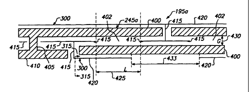
Fig. 6 shows another embodiment 195a of the gradient sheet, having a central
uni-
form resistive layer 205 (shown in Fig. 5) of, for example, two hundred ohms
per square.
Positioned along each edge of the surface of gradient sheet 195a is resistor
chain 245a
formed of a series of overlapping conductive strips 400. Using these strips
400 and the
resistivity of resistive layer 205, the specific resistance of resistor chain
245a can be tailored
for a particular application and distribution of voltages along the edges of
gradient sheet
195a. Typically, conductive strips 400 are physically attached to resistive
surface 205 by
depositing a conductive material, e.g., silver, in the appropriate pattern. A
conductive cor-
ner tab (not shown) applies a voltage to the end of resistor chain 245a, and a
conductive
lead (not shown) typically connects the conductive corner tab to a tab (not
shown) at ano-
ther location of gradient sheet 195a. The conductive comer tab is connected to
appropriate
external circuitry (as within circuitry 110) for supplying the voltage source.
A portion of an
overlapping conductive strip 400 is in a generally spaced relationship with at
least a portion
of another overlapping conductive strip 400 to produce an overlapped resistive
region 402.
Thus, at least one pair of spaced conductive strips 400 provide generally
opposed bound-
aries for defining overlapped resistive region 402 between spaced conductive
strips 400.
At least a portion of one of strips 400 is parallel or generally parallel to
at least a
portion of another strip 400. Additionally, strips 400 are positioned on and
electrically
connected to resistive layer 205 (shown generally in Fig. 5) of gradient sheet
195a.
A conductive lead 405 connects a T-shaped electrode 410 to an overlapping
conductive strip 400. Conductive leads 405, along with resistor chain 245a,
provide the
appropriate reference voltage to T-shaped electrodes 410. The length and
spacing of T-
shaped electrodes 410 are chosen to compensate for any cumulative voltage drop
along
resistor chain 245a, portion which is perpendicular to the current flow on
resistive layer
205. Stated alternatively, the spacings and effective lengths of T-shaped
electrodes 410 are
selected to produce a voltage gradient at each T-shaped electrode to
compensate for any
voltage drop that occurs along resistor chain 245a. Overlapping conductive
strips 400,
conductive leads 405, and T-shaped electrodes 410 each have, e.g., a width of
about 0.5
mm, and all are formed, e.g., by screen printing and curing silver frit in the
desired pattern.
-15-
CA 02314125 2000-06-12
WO 99/30272 PCTIUS98/26448
As shown in Fig. 6, insulation regions 300 are formed adjacent to overlapping
conductive strips 400, conductive leads 405, and T-shaped electrodes 410. An
insulating
region 300 extends into and terminates in an overlapped resistive region 402
from outside
of overlapped resistive region 402. Insulation region 300 has, for example, a
width of about
50 m. According to this particular embodiment of the present invention,
insulating region
300 includes an insulating region portion 415 which extends into and
terminates in an over-
lapped resistive region 402, and an insulating region portion 420 which is
outside over-
lapped resistive region 402. Overlapped resistive region 402 is generally a
continuous sec-
tion of resistive layer 205. Insulating region 300 (shown in Figs. 6-10) may
vary in shape or
configuration. For example, insulating regions 300 may be formed as continuous
lines (as
shown in Fig. 6), dashed or discontinuous liens, spacer dots, and as other
suitable shapes
and sizes sufficient to control current flow on resistive layer 205.
Overlapped resistor length L, as indicated by double-headed arrows 425, is
defined
by the distance separating an insulating region portion 415 from another
insulating region
portion 415 in overlapped resistive region 402. Arrow 425 thus represents the
length of a
resistive region 402 which permits current flow therethrough. The separation
distance or
gap G between overlapping conductive strips 400 is further indicated by double-
headed
arrows 430. Accordingly, the resistance between two overlapping conductive
strips 400 is
directly proportional to the resistivity of coating 205 (see Fig. 5) and is
approximated by
Equation (1).
(1) R -_ pG/L
In Equation (1), p represents the resistivity (ohms per square) of resistive
layer 205 (see
Fig. 5) of gradient sheet 195a. Equation (1) is an approximation, since the
actual resistance
may vary due to contact resistance and due to fringing effects at the ends of
an overlapped
resistive region 402. A direct measurement of resistance R of each overlap
structure can be
taken by placing the leads of an ohmmeter between consecutive conductive leads
405. The
width of, e.g. conductive lead 405, may be widened to, e.g. about 2.0 mm, in
order to
facilitate its role as a test point.
The geometry of insulating region portions 415 can be varied to set the value
of L.
From Equation (1), L can be varied to adjust resistance R. If a direct
resistance measure-
-16-
CA 02314125 2000-06-12
WO 99/30272 PCT/US98/26448
ment or if the linearity data (from linearity testing of gradient sheet 195a)
indicates that R is
too small, then laser ablation processes (for example) can be used to reduce
length L,
thereby increasing the value of R. By varying L, the current flow can be
controlled in the
overlapped resistive region. Other methods, such as numerically-controlled
scribing, can be
used to shape insulation regions 300 and insulation region portions 415.
Conversely, if a smaller value of R is desired, then a larger value of L is
used to
define the geometry of portions 415. For example and as best shown in Fig. 6A,
portions
415 have been set to not extend extensively into overlapped resistive region
402. Thus, L,
as represented by double-headed arrow 425', may extend any desired fraction of
the
distance between overlapped boundaries 432,432 which defines the outer
boundaries of
overlapped resistive region 402. As shown above in Equation (1), R is
adjustable by
altering the geometry of insulative regions 300. Thus, overlapping resistor
chain 245a
becomes, in effect, a chain of adjustable potentiometers.
In addition and as shown best shown in Figs. 6 and 6A, the resistance between
a
node in resistor chain 245a and touch region 206 of resistive layer 205 can be
likewise
varied by adjusting distance 433 through alteration of the geometry of
insulative regions
300. Double-headed arrow 433 thus represents a resistive section which permits
current
flow therethrough.
Figs. 6B and 6C illustrate various amendments of insulating region 300, as
seen in a
partial vertical sectional view looking in direction of the arrows and along
the plane of line
315-315 in Fig. 6. An insulating region 300 may be formed in various ways.
Referring
initially to Fig. 6B, insulating region 300 is formed by creating a channel or
void 350a in
resistive layer 205 and above substrate 200, such that a portion of substrate
200 is exposed.
Channel 350a forms an insulating zone which interrupts current flow through
resistive layer
205. Preferably, channe1350a may be formed by removing or altering portions of
resistive
layer 205 with a scribe, more preferably with a laser or any other suitable
like implement.
For example, low-powered, lasers may be used for control-cutting resistive
layer 205 to
form channel 350a therein. Laser ablation of ITO-coated substrate are
performed by, for
example, Optical Coating Laboratory, Inc.
-17-
CA 02314125 2000-06-12
WO 99/30272 PCT/US98/26448
Portions of resistive layer 205 may be removed or altered by other suitable
methods,
such as chemical etching, photo-etching, chemical or acid deposition, masking,
mechanical
etching, welding, high-photon etching, thermal etching, or other suitable
etching methods.
Additionally, the removal of portions of resistive layer 205 typically
requires removal of
resistive layer 205 in multiple locations of gradient sheet 195a (see Fig. 6).
The process of
removal of resistive layer 205 may be iterated if necessary.
Channel 350a may have, for example, a width of about 50 m, as represented by
double-headed arrows 352. The height of channel 350a is represented by double-
headed
arrows 354 and is about equal to the thickness of resistive layer 205. For
example, channel
350a may have a height of less than a wavelength of light. The shallowness of
channel
depth 354 supports low cost processes for removal of resistive layer 205.
As shown in Fig. 6C, the channel in resistive layer 205 may be formed with
different configurations, such as channel 350b. Additionally, in Figs. 6B and
6C the
insulative characteristics of insulating region 300 is partly dictated by the
extent of the
conductivity of substrate 200. Based on the teachings of the present
invention, it also
follows that a dielectric or non-conducting insulative material, such as
glass, can be formed
in the channel of resistive layer 205. Other types of solid, non-conductive
materials which
can be used as insulative material include, but are not limited to,
porcelains, mica,
magnesia, alumina, aluminum silicate, various high polymers (e.g., epoxies,
polyethylene,
polystyrene, PVC, phenolics, etc.) cellulosic materials, cellular rubber,
nylon, and silicon
resins. These materials may be used alone or in combination with other
insulators.
Fig. 7 shows another embodiment of the gradient sheet, generally illustrated
as
195b. A series of conductive strips 500 forms resistor chain 245b. Insulating
region 300
includes an insulating region portion 505 which extends into an overlapped
resistive region
510. Preferably, insulating regions 300 also include an upper insulating
region segment
515 and T-shaped insulating segments 517, all of which are outside of
overlapped resistive
regions 510. Overlapped resistor length (L), as indicated by double-headed
arrows 520 is
defined by the distance separating an insulating region portion 505 in
overlapped resistive
region 510 from another insulating region portion 505 in overlapped resistive
region 510.
Double-headed arrow 520 thus represents a resistive section which permits
current flow
-18-
CA 02314125 2000-06-12
WO 99/30272 PCT/US98/26448
therethrough. The separation distance or gap ) between overlapping conductive
strips 500
is indicated by double-headed arrows 525. Accordingly, the effective
resistance value
between two overlapping conductive strips 500 is also approximated by Equation
(1).
Additionally, the resistances between nodes in resistor chain 245b and touch
region 206 of
resistive layer 205 can be adjusted by setting a resistive section defined by
double-headed
arrows 527.
Gradient sheet 195b, as shown in Fig. 7, may be applicable for predictably non-
linear, low-power sensors with narrow borders. A predictably non-linear sensor
is attained
by use of controller electronics I 10 or driver software which would apply
fixed linearity
correction coefficients to compensate a reproducible non-linearity. Such
driver software is
implemented based on, for example, in WO 97/34273. Preferably, distances 520
and 527
are adjusted to limit the number of variable non-linear correction
coefficients required.
Fig. 8 shows another embodiment of the gradient sheet, generally illustrated
as
195c. A series of conductive strips 550 and insulating regions 555 and 560,
and resistive
layer 205 form resistor chain 245c. Insulating region 300 includes an upper
insulating
section 555, T-shaped insulating sections 560, and comer insulative sections
565. A por-
tion of a conductive strip 550 is in a generally spaced relationship with at
least a portion of
another conductive strip 550 to produce an overlapped resistive region 570.
Upper insulat-
ing section 555 includes insulating subsections 575 which extend into
overlapped resistive
region 570. Similarly, a T-shaped insulating section 560 includes an
insulating subsection
580, while a corner insulating section 565 includes an insulating subsection
585, wherein
insulating subsections 580 and 585 extend into a resistive region 570. The
resistances of
resistor chain 245c can be adjusted by setting values of lengths L1 and L2, as
represented
by double-headed arrows 590 and 595, respectively. Length L1 is set by
adjusting the geo-
metry of insulative subsections 575 and 580 in overlapped resistive regions
570. Length L2
is set by adjusting the geometry of T-shaped sections 560. The geometry of
subsections
575 and 580 and of T-shaped sections 560 may be adjusted by, for example,
laser ablation.
Fig. 9 shows yet another embodiment of the gradient sheet, generally as 195d.
A
series of conductive strips 600 and overlapped resistive region 605 form
resistor chain
245d. Insulating regions 300 include a T-shaped insulating region having an
insulating
-19-
CA 02314125 2000-06-12
WO 99/30272 PCT/US98/26448
subsection 615. Insulating subsection 615 communicates with another insulating
subsection
620 which is generally normal thereto and which terminates in and contacts two
contiguous
opposed overlapping conductive strips 600 within overlapped resistive region
605. A
portion of T-shaped insulating region 610 disposed outside of overlapped
resistive region
605 includes an insulating segment 625 which terminates in and makes contact
with the
same two opposed contiguous overlapping conductive strips 600 outside of
overlapped
resistive region 605.
Insulating regions 300 further include an insulating segment 630 which also
includes an insulating segment 635 terminating in another insulating segment
640.
Insulating segments 635 and 640 are typically disposed in overlapped resistive
regions 605.
Additionally, insulating segment 640 terminates in two opposed contiguous
overlapping
conductive strips 600. The resistances of resistor chain 245d are adjusted by
setting the
lengths of resistive section widths represented by double headed arrows 645
and 650.
Because resistive region 605 is rectangular in shape, Equation (1) more
accurately predicts
the resistance of region 605, and hence simplifies the adjustment of this
resistance.
Note that the resistance of resistive region 605 is independent of any
moderate
registration offsets between conductive regions 600 and insulating regions
300.
Fig. 10 is a top plan view of another embodiment of the Fig. 9 gradient sheet,
generally illustrated as 195e, and having T-shaped insulating region 610
disposed outside of
overlapped resistive region 605. For gradient sheet 195e, insulating segment
625 forms an
angle 0 with a conductive strip 600. The angle 0 value may differ for each T-
shaped
insulating segment 610 in gradient sheet 195e of the same touchscreen sensor.
For
example, sub-segment 627 of insulating segment 625 may be rotated in the
direction of
arrow 627a to increase the value of the angle 0. Sub-segment 627 may be
rotated in the
direction of arrow 627b to decrease the value of the angle 0.
The resistances of resistor chain 245e can be adjusted further by setting the
overlapped resistor spacing (as indicated by double-headed arrows 645), T-
shaped
insulating segment 610 spacing (as indicated by double-headed arrows 650), and
by the
angles 9 formed by insulating segment 625. The resistances between touch
region 206 and
resistor chain 245e will vary as a function of manufacturing variations in the
offset between
-20-
CA 02314125 2000-06-12
WO 99/30272 PCT/US98/26448
conductive electrodes 600 and insulative region 300. By varying the values of
the angle 0,
the rate which this effective resistance changes (as a function of the offset
magnitude) is
altered. Thus, adjustment of the angle 0 provides a design degree of freedom
for reducing
sensor non-linearities caused by manufacturing offset variations.
Fig. 11 shows a top level view of gradient sheet 195d of Fig. 9. The pattern
of
resistor chain 245d of Figs. 9 and 11 simplifies the calculation of the
resistances of resistor
chain 245d, minimizes the effects of manufacturing registration offsets
(manufacturing
variations), and facilitates a simplified iterative feedback loop which
corrects the resistance
values in order to compensate for material variations and/or process
variations.
Refemng now to Fig. 12, a capacitive (AC resistive) embodiment of a
touchscreen,
generally illustrated as 700, is shown according to the present invention. A
substrate 705
(typically glass or plastic) includes a resistive layer 710 (typically ITO or
ATO).
Conductive electrodes 715 are provided and electrically connect to resistive
layer 710.
Insulating regions 720 may be formed by removing portions of resistive layer
710 by laser
ablation or other suitable methods discussed above. A dielectric layer 725 is
formed
directly on resistive layer 710, while a conductive (resistive) coating 730
(e.g., ITO or
ATO) may be applied to the bottom of substrate 705 as a guard electrode.
When the four corners electrodes (not shown) of substrate 705 are driven by an
AC
signal, a fmger 735 "grounded" to a human body functions as a current sink,
thereby pro-
viding a current path from the corner electrodes via capacitive coupling to
grounded finger
73 5. This mode of operation is, in effect, a "current sinking mode" wherein
the four
substrate corner electrodes are excited by an equal voltage level. When
grounded finger
735 is placed in mechanical contact with dielectric layer 725, grounded fmger
735 is
capacitively coupled to resistive layer 710, and changes in the AC currents in
the four
substrate corner electrodes are then observed for determining the location of
the touch of
grounded finger 735. Dielectric layer 725 insures that grounded finger 735 is
in close pro-
ximity with resistive layer 710 without DC contact. For manufacturing process
control,
touchscreen linearity can first be tested in a quasi-DC resistive touchscreen
mode, and
insulative regions 720 are then formed or adjusted accordingly before
dielectric layer 725 is
formed. Conductive coating 730 serves two functions. First, it can act as an
electronic
-21-
CA 02314125 2000-06-12
WO 99/30272 PCT/US98/26448
shield between resistive layer 725 and possible electronic noise sources
located adjacent to
the touchscreen, such as the display device. Second, if conductive coating 730
is driven by
the same AC driving signals which are applied to the four corner electrodes,
then the cur-
rent sinking effects of the stray capacitance between resistive layer 710 and
the surrounding
environment are greatly reduced.
Continuing to refer to the drawings, substrate 200 is provided with resistive
layer
205 which converts physical position information thereon into electrical
signals. A
dimension is then determined for a length of a resistive section which is to
be located in
resistive layer 205. In Fig. 6, the resistive sections (as defined by
distances 425 and 433)
permit the flow of current therethrough from and through resistor chain 245a.
In Fig. 7, the
resistive sections (as defined by distances 520 and 527) permit the flow of
current there-
through from and through resistor chain 245b. In Fig. 8, the resistive
sections (as defined
by distances 590 and 595) permit the flow of current therethrough from and
through resistor
chain 245c. In Figs. 9 and 10, the resistive sections (as defined by distances
645 and 650)
permit the flow of current therethrough from and through resistor chain 245d.
The dimension for a length of a resistive section is determined by electrical
excita-
tion in the resistive layer. Electrical excitation may be provided, for
example, by excitation
voltages or by current injection. More specifically, during the linearity
testing stage, the
electrical behavior of gradient sheet 195 is tested by observing the
electrical field patterns
thereon. Testing of linearity, or more generally, measurement of discrepancies
between
desired and observed voltage gradients, during manufacture is key to realizing
the advan-
tages of the electrode patterns (i.e., resistor chains 245a-245e in Figs. 6-
10, respectively).
Linearity testing may, e.g., involve exciting the four corner electrodes at
corners 270 (see
Fig. 5) with "X", and then "Y", excitation voltages. For each type of
excitation voltages,
voltages at a rectangular grid of points, e.g. 6 by 8, are measured with a
volt meter probe.
Thus, with testing of this type, the electrode designs discussed above provide
an ability to
easily and rapidly adapt to manufacturing variations and speed design
optimization.
Consider a batch process, in particular, what happens after a lot of glass
substrate
has been coated with ITO and provided with the silver-frit pattern of
conductive electrodes.
Using the nominal design geometry for the regions of removed ITO, a small
sampling from
-22-
CA 02314125 2000-06-12
WO 99/30272 PCT/US98/26448
the lot, e.g. 3 substrate units, is further processed and tested for
linearity. In Fig. 6, for
example, the length L may have a first initial value prior to linearity
testing. During linea-
rity testing, the measured discrepancies in the voltage gradients are then
used to determine
desired changes to the resistance values of the resistor elements of the
border electrode
pattern. The geometry of the removed ITO regions is then redesigned to
implement the
desired changes in resistance values of the resistor chains (e.g., resistor
chains 245a-245e).
The resistance values of a resistor chain 245a is tuned, such that, e.g., a
uniform voltage
gradient gradient can be excited on resistive layer 205 (see Fig. 5), i.e.,
linearity is achieved
throughout resistive layer 205. Thus, according to the present invention, the
desired
linearity is achieved by adjusting the resistances of resistive region 402 of
resistor chain
245a in gradient sheet 195a. The modified design for the geometry of the
removed ITO is
then used to process the remaining substrate units of the lot.
The above electrode patterns also provide similar advantages for continuous
processes. By periodically testing linearity of samples from a continuous
production line,
the geometry of the removed-ITO regions can track drifts in the manufacturing
process.
A key observation here is that programmable low-cost manufacturing processes
exist for creating regions of removed ITO (insulation regions 300). These
processes
include, but are not limited to, laser ablation or scribing, for which a
change in design
geometry requires only reprogramming of numerically controlled manufacturing
equipment. In contrast, the silver-frit electrode pattern of resistor chains
245a-245e is most
cost-effectively applied using a screen printing process that does not support
fast
modifications of silver-frit electrode geometry in response to manufacturing
variations.
Algorithms used in the adaptive process of creating insulation regions 300
require
quantitative information on the correlations between voltage gradient
discrepancies and
changes in the resistance values from alternations in removed-ITO geometry of
insulation
regions 300. These correlations may be determined by computer simulations that
numerically solve Poisson's equation for the boundary conditions corresponding
to various
modifications of the electrode design. Alternately, these correlations may be
determined
experimentally by observing voltage gradient discrepancies induced by
alternations in
removed-ITO geometry of insulation regions 300.
-23-
CA 02314125 2000-06-12
WO 99/30272 PCT/US98/26448
Such adaptive processes can compensate for batch-to-batch variations or drift
in the
uniformity of the ITO coating process, line width variations and other
variations in the
silver-frit electrode process, and other sources of variation in the
manufacturing processes,
thereby reducing manufacturing costs.
Furthermore, the easily optimized designs of the invention (including the
electrcle
designs above) may also reduce the time to market for new products.
Additionally, the
invention permits cost-effective production of sensors originating from "last-
minute" or
customized orders. This contrasts with prior art designs for which non-
linearities from the
electrode pattern design, perhaps due to quantitative errors in process-
dependent design
parameters, are difficult to correct.
= Reference is now made to Fig. 10, by way of example, to describe the
adjustment of
the dimension of a length of the resistive sections (as represented by
distances 645 and/or
650). First insulating region 610 is formed in resistive layer 205 (see Fig.
5), while second
insulating region 630 is formed and is spaced at a distance 645 from first
insulating region
610 such that distance 645 defmes the length of a resistive section through
which current
may conduct. First insulating region 610 (or second insulating region 630)
extends to an
overlapped region 605 from a portion of resistive layer 205 (see Fig. 5) which
is outside
overlapped region 605.
If the length of the resistive section, as best represented by distance 645,
is to be
adjusted, then first insulating region 610 may be extended further into
overlapped region
605. This would decrease distance 645 and thus increase resistances of
resistor chain 245e.
Alternatively, first insulating region 610 may extend only slightly into a
portion of resistive
layer 205 (see Fig. 5) which is inside overlapped region 605. Under this
alternative,
distance 645 increases and the resistance of resistor chain 245e decreases.
In Fig. 10, first insulating region 610 is also spaced at a distance 650 from
an
adjacent first insulating region 610. Distance 650 can be adjusted to further
set the value of
the resistance between nodes of resistor chain 245e and touch region 206 of
resistive layer
205. For example, by decreasing distance 650, this resistance increases. By
increasing
distance 650, this resistance decreases.
-24-
CA 02314125 2000-06-12
WO 99/30272 PCT/US98/26448
First insulating region 610 and second insulating region 630 (of insulation
region
300) may be formed by etching a channel 350a or 350b (see Figs. 6B and 6C) in
resistive
layer 205 (see Figs. 6B and 6C again). Preferably, the etching of channel 350a
or 350b is
performed by laser etching or ablation. Alternatively, channel 350a or 350b
(see Figs. 6B
and 6C again) may be formed by numerically-controlled scribing of resistive
layer 205 (see
Figs. 6B and 6C again).
The position touch sensor and method according to the present invention is
applicable to resistive touchscreen (quasi-DC resistive touchscreens) 105, as
shown in Fig.
5, and to capacitive touchscreens (AC resistive touchscreens) 700, as shown in
Fig. 12.
The position touch sensor and method according to the present invention make
possible the following advantages. The invention permits partial compensation
for
manufacturing variations in the ITO coating process, and thus ITO
manufacturing
tolerances can be relaxed, reducing manufacturing costs. Of interest to low-
power touch
system design, higher resistivity values tend to have larger manufacturing
variations. Such
variations can be better tolerated using the present invention. Production of
ITO coatings
with higher resistivity values are possible while maintaining acceptable
linearity
performance. ITO coatings which have higher resistivity values are desirable
in low-power
touch sensors which may be applicable to lap-top/notebook computers and to
PDAs.
In addition, the present invention decreases yield loss and delays in
manufacturing,
since resistor chains (245a to 245e) can be quickly tuned to match the
characteristics of a
particular ITO coating run during the manufacturing process.
Although only certain specific embodiments are described herein, it will be
recog-
nized by persons skilled in the art that the teachings herein permit the
fabrication of other
devices which perform as described above. Thus, while the present invention
has been des-
cribed herein with reference to particular embodiments, a latitude of
modification, various
changes and substitutions are intended in the foregoing disclosure, and it
will be appre-
ciated that in some instances some features of the invention will be employed
without a
corresponding use of other features without departing from the scope of the
invention.
-25-