Note: Descriptions are shown in the official language in which they were submitted.
CA 02314270 2000-07-18
10
Optical Intersatellite Communications System
zo for Transmitting a Modulated Laser Beam
The present invention relates to an optical intersatellite communications
system
for transmittig a modulated laser beam.
z5 Optical intersatellite communications systems are known, which operate with
digital data at a fixed bit rate of, for' example, 1.5 Gbits/s t 3%. Analog
optical
communications systems are also known in many variations. In the case of a
digital
signal, the pulse shape of the signal is always specified within a narrow
tolerance range,
because otherwise the system could not function. A main problem in connection
with the
3o coherent homodyne transmission arises in the synchronization of the local
oscillator laser,
whose phase is to be secured to or locked with the received light wave for
detection and
demodulation purposes. lNith digital systems with a fixed data rate, there is
a simple way
to achieve synchronization by employing the so-called syncbit method, wherein
the data
flow contains a syncbit which, after seventeen bits of "zeros" and "ones", is
in a third state
35 "~.5".
CA 02314270 2000-07-18
-2-
It is now the object of the present invention to provide an improved optical
intersatellite communications system in accordance with claim 1.
Accordingly, the system in accordance with the invention permits the
transmission
s of almost arbitrary analog and digital signals at various data rates up to a
defined
bandwidth over optical intersatellite links, and this in contrast to known
systems, which
only permit the transmis:;ion of digital signals at a fixed prescribed data
rate.
~o
Advantageous embodiments of the invention are recited in the dependent claims.
The invention will be explained in greater detail in what follows by means of
drawings. Shown therein are in:
Fig. 1, a schematic representation of an optical intersatellite communications
~s system in accordance with the invention, having a transmitting element and
a receiving
element,
Fig. 2, a diagram of the degradation of the signal/noise ratio in such a
communications system,
zo
Fig. 3, schematic representations of a syncbit frame in the frequency range
and
the time range,
Ftgs. 4 and 5, block circuit diagrams for explaining the multiplexing of
different
is sub-channels of a base band channel, or respectively a microwave channel,
Fig. 6, a block circuit diagram of a so-called RFE circuit,
ao order,
Fig. 7, a diagram to be used for correcting the non- linearities of the third
and fifth
Fig. 8, a block circuit diagram of an optical intersatellite communication
system in
accordance with the invention,
35 Fig. 9, a schematic representation to explain the correction of non-
linearities,
Fig.10, a block circuit diagram of a first circuit for producing such a
correction,
CA 02314270 2000-07-18
-3-
Fig. 11, a block circuit diagram of a second circuit for producing such a
correction,
and
FIg.12, a diagram for the optimization of such a linearity correction.
The analog system in accordance with Fig.1, having a transmitting element 9
and
a receiving element is defined in the customary manner as a function of the
CNR value
(can-ier-to-noise ratio) arid the CIM value (carrier-to-intermodulation
ratio). A signal Se
~o with a signal-to-noise ratio SNRin is supplied to the transmitting element,
and the
receiving element provides an output signal So with a signal-to-noise ratio
SNRout. The
total SNR value, which determines the dynamic range DR of the link, relates to
the
incoherent addition of noise and intermodulation. Sine- shaped signals are
used for
measuring these analog values, while digital links are specified by digital
signals and SNR
~s or BER values. It is therefore necessary to specify the analog links also
in regard to the
intermodulation. The bit error probability in a digitally modulated sub-
channel at the
output of the system is greater than at its input because of a finite SNR
value. Fig. 2
shows by way of example the CNRlink requirements for a given SNR input value,
and an
acceptable SNR degradation SNRout - SNRin because of the finite SNR value of
the link.
zo With the majority of appliications, .a sub-channel modulation is used in
analog systems.
The sub-channels themselves normally transmit digital data. However, the
entire system
is considered to be analog, because the lnterferences between the sub-channels
reduce
their SNR factor which, because of the non-linearity of the system, is a
property of an
analog system which is not specified in digital systems. In contrast to this,
the invention
is provides a band-limited "'transparent" channel, which constitutes an ideal
analog system.
Communications satellites in geostationary orbits have a frequency band
between 10.7
and 12.75 GHz, wherein most likely a frequency band between 21.4 and 22.0 GHz
will
probably also be employed in the future.
3o FIg. 3 shows that; in accordance with the present invention two separate
ranges of
the bandwidth are used. A first range is reserved for a synchronization
channel 31 of a
narrow bandwidth between 0 and some MHz, f.e. for synchronization frames at
fixed data
rates, wherein in Fig. 3 the spectral output density PSD is represented as a
function of
the frequency f, and the modulation signal amplitude as a function of time.
The
3s synchronization channel 31 contains data, i.e. zeros and ones, and syncbits
in the status
"0.5" for the local oscillator of the receiver. In connection with a phase
modulation
(BPSK: binary phase shift keying) of the lightwave, a data bit "0" will
modulate the phase
CA 02314270 2000-07-18
-4-
of the lightwave 33 for e;Kample by <-90 in the optical modulator on the
transmitter end,
while a "1" adds an amount of 80 to the phase of the lightwave 34. In contrast
thereto,
the "0.5", or respectively the syncbit, adds the amount 0 to the phase of the
lightwave 35.
The receiver can then extract the 0 phase states, i.e. the syncbits, and can
pertorm the
synchronization of the local oscillator.
In this connection it should be noted, that the syncbit must be surrounded by
bits
of symmetrical phase states, because otherwise it could not be detected in the
receiver.
In addition to various sub-channels 1 to n, a syncbit frame channel is
additionally
~o provided, through which first signaling bits 36, at least one syncbit 35
and second
signaling bits 37 are for example transmitted. This syncbit channel 31 is per
se similar to
the syncbit channel of a digital system, but has a much narrower~bandwidth,
for example
of a magnitude of some Mbits/s, instead of Gbits/s.
The difference between digital operation and analog operation lies in the
different
optical phase-locking loops used for synchronization, or OPLL loops (optical
phase-lock
loop synchronization). In a system with a fixed data rate, the OPLL loop is
performed with
the aid of syncbits having the length of a data bit, which are respectively
inserted after the
predetermined number of data bits mentioned. In analog operation, a
synchronization
zo frame of a small bit rate with the syncbits and other auxiliary data is
transmitted, spectrally
separated from the actual useful data. Thus, in accordance with the present
invention,
both modes of operation differ only in the processing of syncbits, in a few
filter functions
and in the processing of the received signal, such as, for instance, with the
clock and data
retrieval in the course of digital operation with a fixed data rate.
On the other hand, a large bandwidth 32 between 10 MKz and 1 GHz is available
for the "transparent link" 32 in the course of this. Within this transparent
band 32, each
signal which spectrally fits in it, can be transmitted, regardless of its
shape, by means of
such a transparent link. In any case, synchronization takes place by means of
the narrow
so channel 31 below the transparent channel 32. The synchronization channel
must have a
frame with syncbits and data bits in symmetrical states, so that the local
oscillator can
achieve the synchronization state.
The syncbit method can be performed with the aid of FPGAs (field-programmable
gate arrays), which are considerably more cost-efficient than the RFASICs
(radio
frequency application- specific integrated circuits), which are required for
syncbit
processing in digital systems with fixed data rates.
CA 02314270 2000-07-18
-5-
The known digital systems are not transparent in the sense of the present
invention, since they must have a stable data rate, for which only deviations
of a few
percent are permissible, and also, because the pulses should be more or less
rectangular, so that the so-called analog signals of arbitrary wave shapes -
for a defined
bandwidth - or digital signals with a data rate different than the data rate
provided, are
basically neither permissible nor transmittable.
The transparent channel has a much greater bandwidth and can transmit every
~o signal, whose spectrum fits into the channel. If it is necessary to
transmit several digital
or analog signals, such as is the case with TV satellite communications, this
channel has
several sub-channels. As represented in Fig. 4, the signals are transmitted
over the
transparent channel 41. A signal can modulate the respective carrier in the
multiplexing
device 42 on the transmitter end in each sub-channel 1, ..: n, before it is
passed on to the
~5 optical link. These modulated carriers can then be multiplexed, and the sub-
channels are
then de-multiplexed and again down-mixed in a demultiplexing device 43 at the
end of the
link. The syncbit frame 44 on the transmitter end is preferably conducted via
a low
bandpass filter to a multiplexer 45 of the device 42, and the syncbit frame 46
on the
receiver end is preferably retrieved via a low bandpass filter by a
demultiplexer 47 of the
zo device 43.
In a satellite, the sub-channels can already be multiplexed into microwave
carriers
of a magnitude of 10 GHz. As represented in Fig. 5, the signals are
transmitted via the
transparent channel 51. On the transmitter end, the sub-channels 52
multiplexed on the
25 microwave carriers can be conducted to a multiplex device 53 on the
transmitter end.
Since the band occupied byr the sub- channels is relatively narrow, for
example less than
1 GHz, this is preferably performed in such a way that initially the modulated
microwave
signal is down-mixed into a band of approximately 10 MHz to 1 GHz. Such a band
is
transmitted via the optical transparent intersatellite link 51 from one
satellite to another,
3o where a demultiplexer device 55 retrieves the syncbit frame 58 by
demultiplexing. The
signal is again up-mixed into the microwave range in order to make possible a
further
microwave transmission, for example from a satellite to the ground. In place
of n base
band signals or sub-channels of a relatively narrow bandwidth, it is also
possible to
transmit a broadband analc>g or digital base band signal at a high bit rate.
CA 02314270 2000-07-18
-6-
The link interface; consists of several parallel base band inputs/outputs, or
respectively of a single broadband inputloutput. If necessary, base band
processors at
the inputs and outputs can convert the parallel, narrow band channels into sub-
channels,
which have been approf>riately multiplexed with sub- carriers, The single
input broad
band plan is used in particular when a signal, which was multiplexed with sub-
carriers,
had already been delivered to the input and therefore additional signal
processing is no
longer necessary, or when a single analog signal of large bandwidth, or a
digital data
signal at a high bit rate, has to be transmitted.
The homodyne FIFE receiver (receiver front end) in accordance with Fig. 6
consists, for example, of a conventional balanced receiver. The received light
61 and the
laser light 62 of a local oscillator 63 are coupled in an optical hybrid
coupler 64 and
thereafter detected by means of two photodlodes 651, 652. The photo flows from
these
photodiodes are then added in an adder 66 and converted in a transimpedance
amplifier
67 into a voltage. An A(3C (automatic gain control) amplifier 68 finally
provides the
amplified signal 69. A signal 631 from a syncbit processing and OPLL control
unit is
provided to the local oscillator.
zo The diagram in Ftg. 7 Is used for calculating the increase of the
intermodulation IM
in dB in the band center as a function of the number n of carriers through a
link, which
has non- linearities of the third and fifth order, for which the following
equations, which
can be used for n > 9, also apply..
IM3 = 10*log 1C)(1.5*n2) (3rd Order)
IM5 =10*log 10(0.24*n''~°) (5th Order)
The approximation values of the third and fifth order are identified by *, or
3o respectively in Fig. 7. 'The solid lines correspond to the exact values.
Conventional
optical communications systems operate with direct or indirect intensity
modulation. In
the first case, the laser diode injection flow is modulated. With indirect or
external
intensity modulation the laser acts as a CW source, and the beam is modulated
by means
of an external modulator, for example of the Mach-Zehnder type. Detection is
performed
either by measuring the intensity of the modulated light by means of a
photodiode (direct
detection or DD), or coherently, i.e. with the aid of a local oscillator and
subsequent
mixing in a photodiode. Such DG systems are not very sensitive in actual use.
CA 02314270 2000-07-18
-7-
In connection with links having large losses, for example with intersatellite
links,
only coherent systems corn assure the required sensitivity. If the resultant
intermediate
frequency of the coherent mixing process is zero, this is called "homodyne"
detection, if
not; it is called a heterodyne one. Homodyne designs are generally more
sensitive, but
the heterodyne ones are easier to construct. The most sensitive known type is
the
homodyne phase modulation (PM).
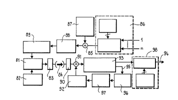
The communications system in Flg. 8 comprises an electro- optical phase
no modulator 81 for modulating the laser light of a TX laser 82, and for
forwarding the
modulated light to the end 83 of a transmission system or link, which
transmits the laser
beam 84. A data signal unit 86 on the transmitter end and a syncbit unlt 87
are
connected to the linkage circuit 85. On the output side, the circuit 85 is
connected with an
electro-optical modulator driver 88, which is connected wia a correcting
circuit 89 with the
ns input of the electro-optical phase rnodufator 81. The data signal unit 86
on the transmitter
end can have a converter with the required mixers, filters and local
oscillators in order to
up-mix the sub- channel signals 1, ... n on the input side. The syncbit unit
87 is provided
for syncbit generation anti filtering. The modulator driver 88 comprises an
amplifier with a
preamplifier, and the correcting circuit 89 Is preferably employed as a pre-
distortion
eo linearizer. A coupling circuit 91, which is also connected with a local
oscillator laser, or
LO laser, 82 at the input side, and whose output signals are provided to an
optical RX
receiver pre- stage 93 which, besides the data signals 94, also provides a
syncbit signal
95, which is passed on via a filter 96 to a syncbit OPLL circuit 97, is
connected to the
other end 90 of the link. ~4 data signal unit 98 on the receiver end can be
provided for
a.5 these data signals, which also has a converter with the required mixers,
filters and local
oscillators in order to down-mix the sub-channel signals on the output side.
The most
important distortion source because of intermodulation results from the so-
called Mach-
Zehnder interterometer, consisting of a phase modulator and EFC (front end
coupler)I
photodiodes. The most important noise source is the shot noise of the RFE
(receiver
so front end)/LO laser.
The communications system in accordance with the present invention comprises
an optical phase-locking loop, also called OPLL (optical phase-lock loop), and
a local
oscillator, for whose synchronization in case of an analog modulation two
methods are
a5 provided, wherein in accordance with one of these a residual pilot carrier
is used, and with
the other a so-called sync;bit technique. With the preferred syncbit
technique,
synchronization bits as well as reference bits are transmitted in a narrow
spectral window
CA 02314270 2000-07-18
-8-
outside of the transmission bandwidth in order to achieve an OPLL phase
synchronization. This synchronization channel can also be used for signaling
and
network control purposes.
Since the system ins accordance with the invention is designed for
transmitting any
arbitrary signals, higher demands are preferably made on linearity than with
employment
with digital signals of a fixed transmission rate. If, for example, two main
carrier signals of
the frequency f1, or respectively f2, and a further carrier signal of the
frequency f3 = 2.f2 -
f1, are transmitted, an intermodulafion product of the frequency f3 is
generated by a
~o system non-linearity of a non-even order. In a digital system with a fixed
data rate, or in a
system operating in a digital mode in accordance with the present invention,
such static
non-linearities do not cause any loss in the transmission quality, even if
they are very
strong, such as when limiters are used. However, the digital systems with a
fixed data
rate must be low-noise in order to achieve great ranges. But the analog
systems must be
~5 low-noise and very linear at the same time, i.e. they must have a great
dynamic range.
In accordance with the present invention, a coherent optical phase modulation
is
preferably employed for both cases to achieve a high degree of sensitivity. In
connection
with systems with fixed data rates, this is then called coherent BPSK
(coherent binary
zo phase shift keying), in contrast to caherent phase modulation (coherent PM)
in the analog
case. In the case of a cohE:rent transmission, the receiver must down-mix the
received
phase-modulated lightwave; to an intermediate frequency with the aid of a
local oscillator.
If this intermediate frequency is zero, the lightwave is demodulated in
accordance with the
so- called homodyne method with the aid of a photodetector directly following
the mixing
z5 with the local oscillator. In accordance with the present invention, this
homodyne method
is preferably used in both cases - analog and digital -, since it is the most
sensitive.
To increase the dynamic range of the link, the optical phase modulator 81, in
which the non-linearity mainly is created, can be linearized with the aid of
an electronic,
3o broadband pre- distortion li~nearization circuit 89 which, for compensating
the sine-like
characteristics of the mixinc~ldetection process, has an arc-sine transmission
characteristic.
CA 02314270 2000-07-18
-9-
The non-linearity of the phase modulator/receiver combination results from the
mixture in the balanced receiver photodiodes.
The following applies for the received laser light field:
Etn (t) - Ein.osln[CO;nt + cp(t)~
wherein ~(t) is the modulated phase.
The following applies for the local oscillator laser field:
ELo (t) = ELo,osln[U~Letl
~o The photo flow, i.e.. the intensity detection of E,n (t) + ELo (t)
Idet(t) - Idet.o Sln[(fin - (~Lo)t '~ ~(t)~
When the phase lock loop has achieved synchronization, cup, and cu~o are
equal, so
~s that (cup, - cu~o) disappears:
idet.syn~(t) = idet.osin[~P(t)l
The detected signal or the photo flow are not proportional to the modulation
voltage, which corresponds to the phase um~(t) = cp(t), but to a sine. It is
distorted in a
zo non-linear manner. The sine- shaped distorted signal approximately results
from a Taylor
series, as follows:
Idet,sync - Idet.o Sln[C~~ - Idet,o [~ - ~3~31 'E' cp5~51 - ...~ = b~ X + 1~3
X3 'I' bs X5 + ...
If the modulation signal, which is proportional to the phase cp , is pre-
distorted by
25 means of an arc sine function, the detected flow will be a linear function
of the
modulation:
Idet,sync,pred - Idet,o,pred sin[arcsin(cp)] = cp
The arc sine function also results from a Taylor series, as follows:
umod.P~(t) umod.o.IxedarCSln[umod,pred(t)~umod,o.P~ umod.o,predarCSln[X~ -
- umod,o.P~[X + X3~Ei + 3x5140 + ...] = a,x + a3x3 + asx5 + ...
CA 02314270 2000-07-18
-10-
Fig. 9 shows an approximation of the functions 890 and 810 of the linearizer,
or
respectively of the modulatorlreceiver, which result in a linearized
combination. The
signal 891 corresponds to the input voltage of the circuit 89 (Fig. 8), and
the signal 811 to
the output voltage of the phase modulator 81 (Fig. 8), or respectively of the
receiver.
In order to compensate the distortions of the third and fifth order, the
relationship
between the coefficients a~, a3 and a5 are of importance. The following three
approximation methods can be employed for the pre-distortion linearization:
a) Antiparallel Schottky diode circuit as the non- linearity:
As represented in Fig.10, the input signal 101 is divided into a linear branch
110
and a non-linear branch 120, in which the non-linearities of the third and
fifth order are
generated by a pair of antiparallel Schottky diodes 103. Since the non-
linearity of a
Schottky diode has an exponential behavior, the non-linearity of an
antiparallel Schottky
diode pair also has an exponential course, namely without even terms and
therefore in
the form:
x + x'/3! + x5/5!
Two damping members 102 and 104 with amplification factors g2, or respectively
g4, are also present in the non-linear branch 120, which permit the control of
the
coefficients of the third and fifth order:
as = 9z' 9a ~ 3! as = 92° 9< ~5!
Known linearizers of the third order only use one damping member corresponding
to the attenuator 104. Therefore the non- linearity of the fifth order cannot
be
compensated, except if the circuit to be linearized has an exponential non-
linearity. An
so aftenuator 105, a variak~le phase shifter 104, and a variable delay circuit
107 have been
connected in series in the linear branch 110. The attenuator 104, as well as
the phase
shifter 104, and the delay circuit 107 permit a compensation of the
coefficients a~ of the
first order. In accordance with the invention, the circuit with the attenuator
102, known
per se for a linearization of the third order, permits the use of an
exponential non-polarity
for the generation of any arbitrary positive non-linearities of the third and
fifth order, and
therefore the compensation of circuits having almost arbitrary non-linearities
of the third
and fifth order, in order i:o supply a linearized output signal 109.
CA 02314270 2000-07-18
-11-
b) Compensation of a rather weak non-linearity by means of a negative sine-
shaped non-linearity in accordance with Fig. 11, which shows an approximation
of the
functions 895 and 815 of the linearizer, or respectively of the
modulator/receiver, for
s resulting in a linearized combinatian. The signal 896 corresponds to the
input voltage of
the circuit 89 (Fig. 8), and the signal 816 to the output voltage of the phase
modulator 81
(Fig. 8), or respectively of the receiver. A sine-shaped non-linearity can be
approximated
by a tanh function. The tanh function can be produced by a cascaded circuit of
two
bipolar differential amplifiers, wherein the first one is excited non-
linearly, and the second
~o linearly. The difference between two collector currents with a constant
sum, which are
exponentially dependent from the input voltage, produces the approximation
tanh = sine.
In accordance with the present invention, such a "sine" circuit, known per se,
can be used
for improving the linearity in accordance with the structure represented in
Fig. 11.
15 C) CMOS circuit. 'the integrated CMOS (cross-coupled differential pairs)
circuits
have a voltagelcurrent non-linearity of the form
~(V~ - ~1 V - u~(1 - UZ/C2~~Z
zo which, with a suitable selection of the coefficients c1 and c2 by means of
transistor
scaling, approximate the arc sine function:
i(u~=a+u'/6+3us/40+...
z5 Fig. 12 shows the dynamic SNR range as a function of the optical modulation
index OMI, wherein OMI = 1 corresponds to a phase angle of 90 . The
representation in
Fig. 12 relates to fixed values of the signal output (-53 dB), of the output
of the local
oscillator (3 mW), the nurnber of ;sub-channels (12) and the bandwidth (36
MHz; total
bandwidth = 500 MHz). In the diagram in accordance with Fiig. 12, CIM is the
3o carrier/intermodulation ratio, CNR is the carrier/noise ratio, and CNRtot
the ratio between
the carrier and the sum of noise and intermodulation, namely CNRtot(lin)
linearized,
CNRtot(unlin) non-linearized, and CNRtot(req) desired. In Fig. 12, the maximum
of the
curve CNRtot(lin) is clearly greater than the maximum of the curve
CNRtot(unlin)~ From
this results the possibility of a transmission via the "transparent" channel
in accordance
3s with the present invention, which therefore permits a simultaneous
suppression of the
intermodulation products of the third and fifth order to a large degree.