Note: Descriptions are shown in the official language in which they were submitted.
CA 02314323 2000-07-21
-1-
AC POWER BACKFEED PROTECTION FOR INVERTER CIRCUITS
BACKGROUND OF THE INVENTION
1. Field of Invention
This invention relates to protection circuits for inverters and more
particularly
to methods and apparatus for preventing power backfeed in inverter circuits
having a switching stage for supplying AC power to an output path of the
inverter circuit.
2. Description of Related Art
Electrical inverters are often used for providing alternating current power to
electrical appliances, in places where alternating current is not available
from
a utility supply. Common places of use include recreational vehicles and
powerboats, for example. Most inverters are powered by batteries and the
output of these inverters are often connected to an alternating current (AC)
bus. Alternate connection between the AC utility and the inverter is usually
required, so that the user may use the same appliances in the same outlets,
by selectively supplying power from the inverter, or from the utility.
Alternate
connection between these two sources is usually provided through a relay or
transfer switch.
The use of a relay or transfer switch, however, creates problems, especially
if
a reactive load is being supplied by the utility and then the transfer switch
is
thrown, to alternatively supply power from the inverter. Relay contacts or
transfer switch contacts experiencing this condition may draw an electrical
arc
for a short period of time while the transfer contacts settle in favour of the
inverter. If arcing occurs during this period, power from the AC utility can
be
backfed into the inverter, possibly damaging the inverter and particularly the
switching devices in the inverter.
CA 02314323 2000-07-21
-2-
What would be desirable therefore, is a device which limits AC power
backfeed into an inverter, especially during source switching by a relay or
transfer switch.
SUMMARY OF THE INVENTION
The present invention addresses the above need by providing an apparatus and
method for preventing power backfeed into an inverter circuit having a
switching
stage for supplying AC power to an output path of the inverter circuit. In
accordance with one aspect of the invention, the method may involve sensing a
current condition in the output path and limiting current in the switching
stage
when the current condition meets a criterion. This may be achieved in one
embodiment through the use of a current sensor which senses the current
condition in the output path and through the use of a switching stage current
limiter operable to limit current in the switching stage when the current
condition
meets a criterion.
The current sensor may sense an instantaneous value of alternating current in
the output path and may comprise a current transformer in the output path. A
resistor may be connected to the current transformer to produce a voltage
representative of current in the output path.
The switching stage current limiter may comprise switching devices in the
switching stage of the inverter circuit. It may also comprise a gate drive
controller for controlling the transmission of gate drive signals from the
inverter
circuit to the switching devices in the switching stage, in response to the
current
condition. Preferably, the gate drive controller is operable to control the
gate
drive signals to cause at least some of the switching devices to be placed in
a
non-conducting mode.
The switching stage current limiter may comprise a condition determiner for
determining the condition sensed by the current sensor. The condition
determiner may comprise a condition comparator in communication with the
gate drive controller for comparing an output of the current sensor with a
CA 02314323 2000-07-21
-3-
reference to cause the gate drive controller to cause at least some of the
switching devices to be placed in the non-conducting mode when the output of
the current sensor is within a range.
The current sensor may include a current to voltage converter operable to
develop a sense voltage in response to instantaneous current in the output
path
of the inverter circuit.
The condition comparator may have a voltage summing circuit for adding a
common mode voltage to the sense voltage and may further include first and
second voltage comparators connected to cause the gate drive controller to
place at least some of the switching devices into the non-conducting mode when
positive or negative excursions of the sense voltage exceed high and low
reference voltages respectively.
The condition determiner may include a latch activated by the condition
comparator to cause the gate drive controller to hold at least some of the
switching devices in the non-conducting mode.
Preferably, a current time rate limiter is provided in the output path, for
limiting
alternating current therein. The current time rate limiter may be operable to
time
rate limit alternating current in the output path to a value sufficiently high
to
permit the inverter circuit to respond to changing load conditions and
sufficiently
low to permit the switching stage current limiter to operate, before damaging
alternating current is conducted in the output path, and in particular the
switching devices. A current time rate limiter may be provided by an inductor.
In one embodiment, the current sensor may be comprised of resistors in series
with switching devices of the switching stage of the inverter circuit.
In accordance with another aspect of the invention, there is provided an
apparatus for preventing power backfeed into an inverter circuit having a
switching stage for supplying AC power to an output path of the inverter
circuit.
The apparatus may comprise provisions for sensing a current condition in the
CA 02314323 2000-07-21
-4-
output path and provisions for limiting current in the switching stage when
the
current condition meets a criterion.
In one embodiment, backfed AC power is limited by an inductor in the rate of
rise of current fed back into the switching stage of the inverter circuit. A
current
sensing device senses current in the output path and compares it with a
reference value to determine whether or not it is within a range. If it is not
within
this range, a signal is communicated to the gate drive controller which
prevents
gate drive signals produced by the inverter, from reaching the switching
devices
of the switching stage. This prevention of gate drive signals from reaching
the
switching devices occurs very quickly, before the damaging AC backfeed power
can reach a level sufficiently high to damage the switching devices. Thus, the
rate of flow of AC backfeed power is limited to permit AC backfeed power
protection circuitry to operate quickly to prevent AC backfeed power from
reaching damaging levels.
Other aspects and features of the present invention will become apparent to
those ordinarily skilled in the art upon review of the following description
of
specific embodiments of the invention in conjunction with the accompanying
figures.
BRIEF DESCRIPTION OF THE DRAWINGS
In drawings which illustrate embodiments of the invention,
Figure 1 is a block diagram of an apparatus according to a first
embodiment of the invention;
Figure 2 is a schematic diagram of a comparator circuit according to the
first embodiment of the invention;
Figure 3 is a logic diagram of a gate drive controller circuit shown in Figure
1; and
CA 02314323 2000-07-21
-5-
Figure 4 is a schematic diagram of current sensing devices in a switching
stage of an inverter, according to a second embodiment of the
invention.
DETAILED DESCRIPTION
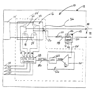
Referring to Figure 1, an apparatus for preventing alternating current
backfeed into an inverter circuit having a switching stage for supplying AC
power to an output path of the inverter circuit according to a first
embodiment
of the invention, is shown generally at 10. The inverter circuit itself is
represented schematically at 12 and it will be appreciated that in this
embodiment the apparatus 10 is incorporated within the inverter circuit 12.
Generally the inverter circuit has a power supply circuit which is usually a
DC
supply circuit 14 which supplies power to the switching stage 16 of the
inverter circuit 12. The switching stage 16 includes a plurality of switching
devices 18, 20, 22 and 24 which may be Metallic Oxide Semiconductor Field
Effect Transistors (MOSFETs), for example, which receive power from the
power supply 14 and provide alternating current at a switching stage output
shown generally at 26. The inverter produces gate drive signals on signal
lines 28, 30, 32 and 34 and these gate drive signals control the operation of
the switching devices 18 to 24, to cause AC power to be produced at the
switching stage output 26. The switching stage output 26 and the switching
devices 18, 20, 22 and 24 connected to the output 26 as an output path 36 of
the inverter circuit 12. The output path 36 is terminated in an output port
38,
from which AC power may be supplied to an AC bus 40 or AC appliance, etc.
Generally, the apparatus 10, according to the first embodiment of the
invention includes a current sensor 42 which senses a current condition in the
output path 36, and further includes a switching stage current limiter shown
generally at 44, operable to limit current in the switching stage 16 when the
current condition sensed by the current sensor 42 meets a criterion.
In this embodiment, the current sensor 42 includes a current transformer 46
having a primary winding in series with one leg 48 of the output path 36. A
CA 02314323 2000-07-21
-6-
suitable current transformer has a 1:1000 turns ratio. A suitable device is
provided under model No. LD50 by Amecon Inc. of California, U.S.A. A
secondary winding 50 of the current transformer is connected in parallel with
a
resistor 52 such that a sense voltage is produced on a signal line 54,
representing an instantaneous value of alternating current in the output path
36. This sense voltage is provided to a current condition determiner 56 which
determines a condition sensed by the current sensor 42 and communicates
the sensed condition to a gate drive controller 58 which is operable to
control
the gate drive signals on signal lines 28, 30, 32 and 34 produced by the
inverter circuit 12 to cause at least some of the switching devices 18, 20, 22
and 24 to be placed in a non-conducting mode. Effectively, the current
condition determiner 56 controls the operation of the gate drive controller 58
in response to the current condition sensed by the current sensor 42.
The current condition determiner 56 generally includes a comparator 60
ultimately in communication with the gate drive controller 58, for comparing
an
output of the current condition sensor 42 with a reference to cause the gate
drive controller 58 to cause at least some of the switching devices 18, 20, 22
and 24 to be placed in the non-conducting mode when the output of the
current condition sensor 42 is within a range. This range may be about 75
amperes or above, in an 800 watt inverter having a destruction threshold of
approximately 140 amperes, for example.
Preferably, the current condition determiner 56 includes a latch 62 which is
activated by the condition comparator 60 to cause the gate drive controller 58
to hold at least some of the switching devices 18, 20, 22, and 24 in the non-
conducting mode.
Referring to Figure 2, in this embodiment, the current condition determiner 56
includes a voltage summing circuit shown generally at 70 for adding a
common mode voltage to the sense voltage produced on signal line 54. The
common mode voltage is provided by a reference source 72. Effectively, the
voltage summing circuit 70 serves to shift or add a DC offset to the sense
CA 02314323 2000-07-21
-7-
voltage on signal line 54, to allow positive and negative excursions of the
sense voltage to be sensed using first and second voltage comparators 74
and 76 operating off of a single polarity power supply. The summing circuit 70
could be omitted if a dual polarity power supply is provided.
The first and second voltage comparators 74 and 76 are connected to cause
the gate drive control circuit 58 shown in Figure 1 to place at least some of
the
switching devices into the non-conducting modes if positive or negative
excursions of the sense voltage exceed high and low reference voltages
produced by reference sources 78 and 80, respectively. The high and low
reference voltages may represent +75 amperes and -75 amperes
respectively, for example. When such conditions occur, the output 82 or 84 of
the respective comparator 74 or 76 causes an active low danger signal to
become active, and this danger signal is ultimately communicated to the gate
drive controller 58, through the latch 62 shown in Figure 1.
Referring back to Figure 1, when the danger signal becomes active, the latch
62 holds its output signal active to produce a shut down signal on a signal
line
86 for receipt by the gate drive controller 58.
The gate drive controller 58 is shown generally at 90 in Figure 3 and includes
transistor-implemented logical "AND" circuits 92, 94, 96 and 98, each
respectively controlled by the shut down signal for producing new gate drive
control signals 100, 102, 104 and 106, by effectively gating, whether or not
the gate drive control signals 28, 30, 32 and 34 are communicated to
respective switching devices,
It will be appreciated that it takes time for the effect of current in the
primary
winding 46 of the current transformer to be noticed at the gate drive signals
100, 102, 104 and 106 due to delays in the operation of the intervening
circuitry including the comparator 60, the latch 62 and the gate drive
controller
58. Consequently, an inductor 110 is placed in series in the output path 36,
to
time rate limit current in the output path. The inductance of the inductor 110
is
chosen such that the rate of change of current in the output path 36 is
CA 02314323 2000-07-21
_$_
sufficiently high to permit the inverter circuit to respond to changing load
conditions, and sufficiently low to permit the switching stage current limiter
44
to operate, before damaging alternating current is conducted in the output
path 36 and ultimately conducted through the switching devices 18, 20, 22
and 24. In this embodiment, for an 800 to 1500 watt inverter circuit, an
inductor having an inductance of approximately 25 microhenries is used to
provide current limiting to approximately 10 amperes per microsecond.
Typically, the time for the intervening circuitry of the current condition
determiner 56 and the gate drive controller 58 is approximately 1 or 2
microseconds.
Referring to Figure 4, in an alternative embodiment, the current sensor 42
may be replaced by resistors 120, 122, 124 and 126 in series between
respective switching devices 18, 20, 22 and 24 and the switching stage output
26. In this case, individual currents through respective individual resistors
120, 122, 124 and 126 may be monitored and compared with four separate
comparators of the type shown at 60 in Figure 3, wired in a logical OR
relation, to produce the active low danger signal which is supplied to the
latch
62.
It will be appreciated that with an embodiment described herein the power
drawn from the output 38 of the inverter circuit is typically limited by the
power
supply capacity of the inverter circuit and is usually limited to a
significantly
low value, which will not burn out the switching devices 18, 20, 22 and 24.
However, if the output 38 is connected to an AC bus 40, the AC bus 40 may
attempt to supply current into the inverter circuit, i.e., in a direction from
the
output port 38 to the switching stage 16. Since an AC bus 40, if connected to
a utility supply, effectively acts as an infinite current source with zero
impedance, extremely high currents can be received at the switching stage
16, burning out the switching components 18, 20, 22 and 24, especially during
relay, transfer switch operation. However, using the embodiments indicated
above, the inductor 110 limits the rate of rise of current flow from the
output
port 38 to the switching stage output port 26 and the current sensing device
CA 02314323 2000-07-21
_g_
42 senses backfeed current which is outside a predefined range such as
provided by the comparator 60, and causes the gate drive controller 58 to
place the switching devices 18, 20, 22 and 24 in the non-conducting mode,
whereby they are all placed in a high impedance state and inoperable to
conduct current. Thus, AC power backfeed is prevented from damaging the
switching devices 18, 20, 22 and 24.
While specific embodiments of the invention have been described and
illustrated, such embodiments should be considered illustrative of the
invention only and not as limiting the invention as construed in accordance
with the accompanying claims.