Note: Descriptions are shown in the official language in which they were submitted.
CA 02314375 2000-07-24
Manfra I-17-13-45 1
THIN FILM RESONATOR APPARATUS AND METHOD OF MAKING
SAME
BACKGROUND OF THE INVENTION
1. Field of The Invention
This invention relates to thin film resonators (TFRs) and a method of making
TFRs.
2. Description of Related Art
TFRs are thin film acoustic devices which can resonate in the radio frequency
to microwave range, for example, .5 to 5 Gigahertz (GHz), in response to an
electrical
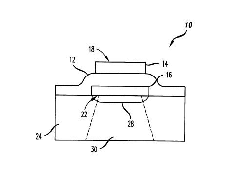
signal. FIG. 1 shows a typical TFR 10 with a piezoelectric film 12 between a
first
electrode 14 and a second electrode 16 which apply an electric field to the
piezoelectric film 12. T'he film 12 is made of a piezoelectric crystalline
material, such
as zinc oxide, aluminurr~ nitrite (A1N) and other piezoelectric crystalline
material,
which exhibits a piezoelectric effect. 'The piezoelectric effect occurs when
the
peiezoelectric material expands or contracts in response to an electric field
applied
across the piezoelectric material, for example by the first and second
electrodes 14
and 16, or produces an electric field in response to mechanical stress or
strain applied
to the piezoelectric material. If the electric field across the film 12 is an
alternating
:Z0 electric field having frequency components corresponding to resonant
frequencies of
the film 12, the film 12 will vibrate at the resonant frequencies (e.g. a
fundamental
frequency and harmonics), the fundamental frequency of which is defined for a
film
of uniform thickness as the acoustic velocity (v) in the film 12 divided by
two (2)
times the thickness (t) o:Pthe film or fT=v / 2t. The film 12 will
mechanically vibrate
:?5 at the resonant frequene:ies which in turn produces an alternating
electric field at the
resonant frequencies.
The first and second electrodes 14 and 16 are typically of metal, such as
aluminum. The acoustic; impedance mismatch between the first electrode 14 and
the
air creates a first acoustic reflecting surface 18 at the interface between
the top surface
30 of the first electrode 14 a.nd the air. A second acoustic reflecting
surface 22 can be
CA 02314375 2000-07-24
Manfra 1-17-13-45 2
established at an interface between the second electrode 16 and a substrate 24
(or air
if a portion of the substz~ate 24 under the film 12 is removed).
Alternatively, acoustic
reflecting layers) can be created between the second electrode 16 and the
substrate 24
to suppress unwanted frequencies, such as harmonics of the fundamental
frequency.
The acoustic reflecting J.ayer(s) can be formed from a material having desired
characteristic acoustic impedance(s) and with the proper dimensions to provide
desired reflection chara<;teristics for the second reflecting surface at the
interface
between the second electrode 14 and the acoustic reflecting layers. As such,
the
acoustic reflecting layers can reflect desired frequencies while suppressing
unwanted
to frequencies. An acoustic cavity created between the first and second
reflecting
surfaces and with the proper dimensions establishes a standing wave at the
resonant
frequencies of the piezoelectric film 12. The dimensions of the acoustic
cavity, for
example the thickness o:F the piezoelectric film 12 and the electrodes 14 and
16,
define the operating frequencies for the TFR 10. Energy outside the operating
frequencies of the TFR '.t 0 is lost, while energy within the operating
frequencies is
preserved.
The TFR 10 structure can be formed on the substrate 24, such as a silicon
(Si),
Gallium Arsenide (GaA:>) or other semiconductor substrate, for monolithic
integration
purposes, such as integration with active semiconductor devices. For discrete
2o applications, the TFR 10 is typically formed on other suitable substrates,
such as
quartz, sapphire, aluminium nitride (A1N), or silicon carbide. If the TFR 10
has
acoustic reflecting layer) s), the acoustic reflecting layers) are formed on
the substrate
24 followed by the second electrode 16 which is formed on the reflecting
layer(s). If
there are no acoustic reflecting layers, then the second electrode 16 is
formed on the
2:5 substrate 24, for example using chemical vapor deposition (CVD) or
sputtering. See,
Kern & Vossen, "Thin Film Processes," Vols. I and II, Wiley & Sons. The
piezoelectric film 12 is tihen formed on the second electrode 16, and the
first electrode
14 is formed on top of tine piezoelectric film 12, for example using chemical
vapor
deposition (CVD) or sputtering. To improve the performance of the TFR 10, a
CA 02314375 2000-07-24
Manfra 1-17-13-45 3
portion of the substrate 24 is removed from under the second reflecting
surface 22.
To remove the portion of the substrate 24, the substrate 24 includes an etch
stop 28,
such as a boron doped p+ layer implanted in a silicon (Si) substrate, at the
upper
surface of the substrate 24 adjacent to the bottom of the second electrode 16.
The
etch stop 28 is used to protect the second electrode 16 from a chemical etch
removing
the portion 30 of the substrate 24.
By growing the piezoelectric film 12 on the second electrode, the resulting
piezoelectric film 12 is polycrystalline in that distinct crystals having
different lattice
orientations are present throughout the piezoelectric film 12. Such a non-
uniform or
1o irregular crystalline structure with grain boundaries between the
differently oriented
crystallites or crystal gr,~ins reduces the quality of the piezoelectric film
12.
Two figures of rnerit are used to measure the quality of piezoelectric films:
a
quality factor Q and an ~~lectro-mechanical coupling coefficient. The quality
factor Q
for a TFR is a measure of the resonance quality of the acoustic cavity while
the
coupling coefficient is a. measure of the efficiency of conversion between
electrical
and mechanical energy ~avithin the acoustic cavity. Both of these figures of
merit are
inversely proportional to the acoustic loss introduced by the TFR at the
operating
frequency band. If the piezoelectric film 10 has a polycrystalline structure
with grain
boundaries and other defects, such as point imperfections or dislocations in
the crystal
:Z0 lattice, or poor reflectivity of the reflecting surfaces 18 and 22 for
example due to
surface roughness, acoustic losses can result from acoustic scattering within
the film
12 and acoustic radiation into the surrounding areas of the device 10. Thus,
if the
film 12 is polycrystalline, acoustic losses will be introduced by the film 12,
thereby
producing a lower quality TFR.
z5 TFRs can be used at radio frequency (RF) because piezoelectric films can be
made thin, for example <~t higher frequencies, such as .5-10 GHz, the
piezoelectric
film 12 can be between ..4 and 8 microns in width. Because TFRs produce an
alternating electric field at the resonant frequency in response to an
alternating
electric field having frequency components corresponding to the resonant
frequencies,
CA 02314375 2000-07-24
Manfra 1-17-13-45
TFRs can be used as radio frequency (RF) filter elements. TFR filters have a
distinct
size advantage over conventional RF filters, such as those based on ceramics.
For
example, thin film resonators can have volumes of 1.5 cubic millimeters while
ceramic resonators are iypically not less than hundreds of cubic millimeters
its
volume. At the same time, a ceramic element typically introduces more loss to
the
input signal at the operating frequency band than the TFR. TFR also have
higher
power handling capabilities than surface acoustic wave (SAVE devices, for
example
200 milliwatts vs. 2 waits. As mentioned above, however, TFRs can introduce
losses
to an electrical signal applied to the TFR in part due to the polycrystalline
structure of
to the film 12. Typical TfR fabricating methods produce piezoelectric films
with on the
order of 108 distinct crystalline orientations separated by grain boundaries.
Thus, a need exists for a high quality TFR which introduces low loss to the
electrical signal applied to the TFR.
SUMMARY OF THE INVENTION
The present invention involves a thin film resonator (TFR) produced with an
improved piezoelectric calm which is epitaxially grown on a growing surface,
resulting in a piezoelectric film with less grain boundaries. Epitaxial growth
refers to
the piezoelectric film having a crystallographic orientation taken from or
emulating
so the crystallographic orientation of a single crystal substrate or growing
surface: For
example, by epitaxially growing a piezoelectric film on a single crystal
silicon
substrate as the growing surface, an improved piezoelectric film is produced
with
little or no grain boundaries. In accordance with another aspect of the
present
invention, a method of nnaking a TFR is disclosed in which the piezoelectric
film is
grown on a substrate. Subsequently, a portion of the substrate is removed, and
the
electrodes are deposited on either side of the piezoelectric film.
CA 02314375 2002-12-02
4a
In accordance with one aspect of the present invention there is provided a
method of
producing a thin film resonator apparatus, said method comprising the steps
of: providing a
single crystal silicon substrate; epitaxially growing a piezoelectric film on
said substrate;
removing a portion of said substrate under said piezoelectric fhn; and
depositing an electrode
under said piezoelectric film.
CA 02314375 2000-07-24
Manfra I-17-13-45 $
BRIEF DESCRIPTION OF THE DRAWINGS
Other aspects arid advantages of the present invention may become apparent
upon reading the follow ng detailed description and upon reference to the
drawings in
which:
FIG. 1 shows a general block diagram of a thin film resonator; and
FIGS. 2-4a and '.>-9 show the different levels of development of an
embodiment of a thin film resonator (TFR) according to the principles of the
present
invention; and
FIG. 4b shows example representations of x-ray diffraction peaks for epitaxial
1 o and non-epitaxial piezoelectric film.
DETAILED DESCRIPTION
The invention is described below with respect to an exemplary embodiment of
the thin film resonator ('TFR) and the method of making the TFR. With
particular
t5 reference to FIG. 2, a single crystal silicon (Si) substrate 40 is provided
on which a
piezoelectric film is epit:axially formed for the acoustic cavity of the TFR.
Epitaxial
growth in the context of this invention refers to the formation of a
crystalline film
with a crystallographic orientation taken from or emulating a single crystal
substrate
or an imposed template pattern on a growing surface. For instance, epitaxially
:?o forming the film with a crystallographic orientation taken from or
emulating the
crystallographic orientation of a single crystal substrate or pattern on a
growing
surface can be shown when a uniform, regular or continuous crystallographic
orientation is consistently achieved for piezoelectric films formed under the
same
growing conditions and relative to the same substrate or surface. In certain
5 embodiments, the piezoE;lectric film is epitaxially formed to have a
uniform, regular
or continuous crystallographic orientation based on the uniform, regular or
continuous
crystollographic orientation of the substrate, for example a single crystal
silicon
substrate. Non-epitaxial growth of the piezoelectric film typically leads to
grain
boundaries which contribute to acoustic energy losses within the resulting TFR
and
CA 02314375 2000-07-24
Manfra 1-17-13-45
result in device degradation through aging and fatigue at the grain
boundaries. The
epitaxial growth results in fewer grain boundaries and improved structural
integrity.
Any deviation in a crystal from a perfect periodic lattice is an imperfection.
A
point imperfection is localized at a point in the lattice structure and can
occur due to
chemical impurities, vacant lattice sites and interstitial atoms (extra atoms
not in the
regular lattice). A line of imperfections, such as a dislocation, is a
discontinuity in the
crystal lattice structure. Typically, on either side of the dislocation, the
crystal
orientation has the same: regular periodic arrangement. Arrays of dislocations
can
form grain boundaries between adjoining crystallites or crystal grains which
have
to distinct crystallographic orientations. Non-epitaxial growth typically
leads to grain
boundaries which produce an irregular and discontinuous crystalline
orientation
within the film. Grain boundaries are significant in producing losses and
should be
reduced to reduce losses introduced by the film to the TFR and to improve the
structural integrity of the film. Other defects, such as dislocations, also
contribute to
t 5 losses and should also be reduced. Non-epitaxial growth of piezoelectric
film for
TFRs typically can have. 108 grain boundaries per cmz and 10~°
dislocations per cm2.
The non-epitaxial piezoelectric film is thereby polycrystalline with a
discontinuous
and irregular crystalline structure, and the dislocations are typically
dispersed
throughout the piezoelectric film. A high quality epitaxial piezoelectric film
grown
:?o on an approximately lattice-matched single crystal substrate typically has
very few
(for example less than 1 ~0 distinct crystallographic orientations within the
film) or no
grain boundaries with 105-10~° dislocations per cmz~at the substrate-
heteroepitaxial
interface. The number of dislocations decreases by a factor of two every 2-
3000
angstroms, and the dislocations are typically parallel to or along the
direction of
25 growth.
Epitaxial growth of a piezoelectric film on a substrate can be obtained when
the substrate and the piezoelectric film has a crystalline structure with
similar in-plane
lattice parameters. For example, a film can be epitaxially grown on a
substrate when
the in-plane lattice mismatch between the piezoelectric film and the
underlying
CA 02314375 2000-07-24
Manfra 1-17-13-45 7
material (the substrate upon which the piezoelectric film is being deposited)
is less
than 20%. Lattice mismatch is equal to [(a0/a0(substrate))-1] where a0 and
a0(substrate) are respectively the in-plane lattice parameters of the
deposited thin film
and the material upon which the thin film is deposited.
The crystal orientation of the substrate cam be varied to reduce the lattice
mismatch between the parallel lattice planes of the substrate 40 and the film
to be
deposited on the substrate 40. For exaunple, a Si substrate 40 with a <111>
orientation can be obtained for epitaxially growing a A1N film. A substrate 40
with a
<110> or <100> orientation can also be sufficient. For an explanation of how
to
describe different crystal orientations, see C. Kittel, "Introduction to Solid
State
Physics," John Wiley & Sons, Inc. ( 1967). Other substrates can include
gallium
arsenide, galium nitride amd others.
By providing a substrate 40 with a uniform, continuous or regular periodic
lattice structure, such as a single crystal silicon, with a suitable lattice
mismatch
between the piezoelectric film to be deposited and the substrate, the
piezoelectric film
can be epitaxially formed on the substrate 40 with a reduced number of grain
boundaries. Single crystal Si substrates have zero grain boundaries and zero
dislocations while a single crystal GaAs substrate has zero grain boundaries
and 10-
105 dislocations per cm2. Epitaxial deposition of a variety of materials is
discussed in
:?o Mathews, Epitaxial Growth, Academic Press, 1975. In alternative
embodiments,
other substrates or growing surfaces, for example gallium arsenide, gallium
nitride, or
aluminum oxide, can be used having different, amorphous or even irregular and
discontinuous crystallinE; orientations so long as the piezoelectric film is
epitaxially
formed with the desired continuous, uniform or regular crystalline
orientation. For
5 example, epitaxial growth can occur using grapho-epitaxy, where a growing
surface is
prepared with physical growth sites or structures, such as grooves, pits,
etchings or a
pattern to epitaxially form a film having a particular continuous, uniform or
regular
crystalline orientation. A film can be epitaxially formed over an amorphously
structured material, such. as an oxide (for example aluminum oxide), through
lateral
CA 02314375 2002-12-02
epitaxial growth which starts with the epitaxial formation of the tilm on an
appropriate
growing surface adjacent to the amorphous structure, and the film forms
epitaxially with
respect to the growing surface over the amorphous structure.
By epitaxially growing the piezoelectric film for the acoustic cavity of the
thin film
resonator, the piezoelectric film reduces loss in the TF R due t<> grain
boundaries in the film.
In some embodiments of the TFR, a piezoelectric film for the acoustic cavity
of the film can
include a first piezoelectric film epitaxially grown with respect to a first
growing surface or
substrate adjacent to a second piezoelectric film having a different
crystalline orientation and
epitaxially grown with respect to a second growing surface or substrate.
Moreover, a frst
piezoelectric film epitaxially grown on a first growing surface can be
adjacent to a non-
epitaxially grown film on a second growing surface. In such embodiments, the
first and
second piezoelectric films are different, and/or the growing surfaces or
substrates are
different.
The single crystal Si substrate 40 can be formed from commercially available
single
crystal Si wafers which are about 0.5-1 millimeter thick. ~fo epitaxially form
a piezoelectric
film on the substrate 40 according to an embodiment of the present invention,
a mask 42 is
deposited on the substrate 40, such as a mask of silicon nitride Si3N4. Other
masks could be
used which are resistant to the etch subsequently used on the substrate 40.
The mask 42 can
be deposited for example using low pressure chemical vapor deposition (LPCVD;)
or other
deposition techniques.
As shown in FIG. 3, an etch stop 44 is produced on the substrate 40 for use in
resisting the subsequent anistropic or isotropic etching of the substrate 40.
Depending on the
dopant, the substrate, and the etchant, the type of etch stop can vary. The
etch stop 44 can be
produced by epitaxial growth or ion implantation, for example to produce a
phosphorus or
boron-doped n+ or p+ etch stop 44 having a dopant level of greater than
10z° atoms per cubic
centimeter. Other etch stops or dopant concentrations are possible.
CA 02314375 2002-12-02
()
At FIG. 4a, a piezoelectric crystalline film 46, such as aluminum nitride
(A1N), is
epitaxially grown on the substrate 40. The piezoelectric film 46 can be
epitaxially grown on
the substrate 40 using molecular bean a epitaxy (MBE). lr~ one embodiment, Si
(I 11) is used
as the substrate on which the AIN film is epitaxially firmed with the c axis
of the film along
the direction of growth. To do so, the Si ( I 11 ) substrate is cleaned in
buffered oxide etch
(BOE), spun dry in air, and loaded into the MBE vacuwn. In the MBE vacuum, the
substrate
is heated to 950 degrees Celsius to desorb the residual oxide from the
substrate. T'he clean Si
(11 I ) substrate is lowered to 800 degrees Celsius, whereby the Si ( I 11 ) 7
X 7 silicon surface
reconstruction shows a reflecting high energy electron diffraction (RHEED)
pattern which
indicates a clean ( 1 I 1 ) surface ready for epitaxial growth. The A1N film
is nucleated at a
substrate temperature of 600-80U degrees Celsius to a thickness of 100
angstroms using a
~;rowth rate of 775 angstroms per hour. The substrate is then raised to a
temperature of
920 degrees Celsius for 200 angstroms more growth of'A1N at 775 angstroms per
hour.
Finally, the substrate is further raised to 980 - 1020 degrees Celsius to
complete the growing
of the AIN film again at 775 angstroms per hour.
Because MBE is performed in a good vacuum, for example, better than
1(l~~° Torr, the
film 46 can be produced with less contamination, resulting in Fewer defects.
The defects
produce scattering of the acoustic energy which results in acoustic losses.
Other methods can
be used to epitaxially produce the fzlm 46 on the substrate 40, such as
sputtering and metallo
organic chemical vapor deposition (CVD).
Because the piezoelectric film 46 is epitaxially formed on the substrate 40
which has a
continuous crystalline orientation, the piezcaelectric film 46 is produced
having a continuous
crystalline orientation, such as a single crystal AIN f Im 46, with relatively
few or no grain
boundaries along the substrate. The epitaxial film 46 may have dislocations or
other
imperfections, but these defects can also be reduced ifthe substrate is
epitaxially formed on
the substrate 40 which has suitable lattice mismatch and a continuous
crystalline orientation.
CA 02314375 2000-07-24
Manfra 1-17-13-45 10
The piezoelectric film 46 can be scanned using x-ray diffraction microscopy
to determine if the piezoelectric film is uniformly oriented and has a low
defect
density. The sharpness or width of the diffraction peak can measure whether
the film
is highly oriented, for example a diffraction peak less than 1 degree thick
throughout
the film, indicates a filnn having a continuous crystalline orientation. FIG.
4b shows
an example of an x-ray diffraction peak for an epitaxial piezoelectric film
with a 00
of .5 degree and an intensity of 106 counts. The dashed line shows an example
x-ray
diffraction peak for a non-epitaxial piezoelectric film with a x-ray
diffraction peak
about 3 degrees wide arid an intensity of 104 counts. The intensity of the
peak can
1o provide an indication of the defect density. A diffraction peak with high
intensity, for
example greater than 106 counts of diffracted x-ray photons relative to a
constant flux
applied to the film, indicates indirectly a low defect density. As shown in
FIG. 4b,
typical non-epitaxial film has an intensity on the order of 104 counts. A
transmission
electron microscope (TEM) or defect etching can be used to determine the
defect
density of the film. In using a TEM, a portion of the crystalline material is
sliced off
and thinned down to a tluckness through which electrons can pass. Because the
defects have a different transmission coefficient than the surrounding
material, defects
can be detected by electron counts. Defect etching involves using a chemical
etch to
enhance the film defect:; which have a different etching rate than the
surrounding
:zo material. Then, the defects are simply counted.
As shown in FIts. 5, a portion 47 of the silicon substrate 40 is removed from
under the film 46 using an anisotropic or isotropic etch after removing a
portion of the
silicon nitride mask 42. Depending on the substrate, different etchants can be
used.
With a silicon substrate, an anisotropic etch can be performed using ehylene
damine
procatechol (EDP). For example, EDP at 100 degrees Celsius would give an
etching
rate of silicon at 50-80 micron per hour. An anisotropic etch can also be
performed
using potassium hydroxide (KOH) at 80 degrees Celsius to achieve the same
etching
rate. Alternatively, an i:>otropic etch can be performed for example using
plasma
etching if using a chromium (Cr) mask. The silicon etches typically attack
most
CA 02314375 2000-07-24
Manfra 1-17-13-45 11
metals, including aluminum and aluminum nitride. Consequently, in this
embodiment, the etch stop 44 protects the A1N film 46 from the etch. Dashed
lines
48 show the effects of alifferent types of etches on the substrate 40. Dashed
line 48a
illustrates the effects of an anisotropic etch using for example EDP or KOH,
dashed
line 48b shows the effects of an isotropic etch, and dashed line 48c shows the
effects
of other anistropic etches, for example using reactive ion etching (RIE), to
achieve a
different etching profile. The etch stop 44 acts by not being substantially
etched
under the conditions usc;d to etch the underlying layer.
As shown in FICi. 6, the etch stop 44 and the remaining mask 42 can be
1o removed by reactive ion etching (RIE) with Fluorine chemistry which attacks
the
silicon but stops at the A1N film 46 in this embodiment. In alternative
embodiments,
the etch stop 44 is not removed. Depending on the materials, other etching
techniques can be used.
After the piezoelectric film 46 is exposed, the film 46 and the remaining
substrate 40 are oxidized, for example using thermal oxidation or anodization,
as
shown in FIG. 7. The silicon oxide layer is added to provide electrical
isolation of the
electrodes from the silicon substrate. Non-conducting substrates, such as GaAs
and
aluminum oxide, would not require isolation form the electrodes. In this
embodiment, since the piezoelectric film 46, for example of A1N, has a low
oxidation
rate when compared to the substrate 40, for example of silicon, thin layers 49
and 50
of aluminum oxinitrite (AION;), for example 100-200 angstroms thick, are
produced
on the AlN filin 46. The; silicon substrate is oxidized to form a layer 51 of
silicon
dioxide (SiOz), for examiple of 1000-2000 angstroms thick. The AION layers 49
and
50 on the top and bottom of the film 46 are removed using chlorine based
chemistry
5 which has little effect on the layer 51 of silicon dioxide as shown in FIG.
8. In
alternative embodiments, the layers 49 and 50 can be selectively etched to
remove the
layer 49 and/or the layer 50, or both layers 49 and 50 can be retained.
As shown in FIG. 9, electrodes 52 and 54, such as aluminum or other metal
electrodes, are produced on either side of the film 46 to form a capacitor
with the film
CA 02314375 2000-07-24
Manfra 1-17-13-45 12
46. The electrodes 52 and 54 are deposited by sputtering which is typically
performed using Argon gas as a sputtering gas, for example using a M2000
sputtering
system from Novellas of Santa Clara California, USA. As would be understood by
one of skill in the art, this type of sputtering involves placing an electric
field and
Argon between the TFR. being fabricated and an aluminum (AI) target. The Argon
ions are attracted to the Al target and bombard the A1 target, releasing A1
ions and
neutral species which are deposited on the top and/or bottom (as well as the
substrate
40) of the film 46. Other electrode deposition techniques can be used, such as
chemical vapor deposition (CVD).
t 0 Thus, an improved thin film resonator is produced with less grain
boundaries
to reduce losses introduced by the TFR to electrical signals at certain
frequencies
corresponding to the resonant frequencies of the TFR, for example .1 to 10
GHz. For
other frequencies, the film can be formed with different thicknesses. In
addition to
the embodiment described above, alternative embodiments of the method of
:U 5 fabricating the TFR are possible which omit and/or add steps and/or use
variations or
portions of the described method. Additionally, alternative embodiments of the
resulting TFR are possible which add and/or omit layers and/or structures
and/or use
variations or portions of the described TFR. For example, the layer 48 and/or
49 can
be removed and/or retained before the electrodes 52 and 54 are deposited.
Moreover,
2o additional layers of for example reflecting layers can be included in the
manufacturing of the TFR or subsequently added to the TFR. The TFR is
described
as being fabricated with particular materials and using particular etches, but
alternative materials and etches can be used to fabricate the TFR according to
the
principles of the present invention. For example, other piezoelectric
crystalline films,
a5 such as zinc oxide, as wc;ll as other piezoelectric materials can be used.
The TFR is described with the piezoelectric film being grown on a single
crystal Si substrate but other growing surfaces are possible which epitaxially
produce
a uniform crystalline stnicture in the film based on the crystallographic
orientation of
the substrate or on the growing surface. For example, the film 12 can be
epitaxially
CA 02314375 2002-12-02
13
grown using grapho-epitaxy in which case the electrode surface can be the
growing surface
which has been patterned or textured, for example with a periodic, regular
pattern. The
periodic regular patterned surface can be formed to emulate a surface of a
single crystal
substrate. A regular periodic pattern of mezas and/or grooves can be used as
seeds for the
piezoelectric film using spacing commensurate with the spacing of the lattice
structure of the
piezoelectric film, such as the same spacing or a multiple of the spacing
between the parallel
lattice planes. The pattern can be formed using lithographic and/or etching
techniques.
<Jrowing processes could be similar to those described above crr would be
understood by one
of skill in the art with the benefit of this disclosure. Using I.ECr(~TM, a
substrate or
appropriate growing surface is adjacent to the electrode over which the
piezoelectric film is
grown as would be understood by one of skill in the art with the benefit of
this disclosure.
Alternatively, a single crystal electrode with the appropriate lattice
structure could be used as
an electrode on which the piezoelectric film is grown. As would be understood
by one of
ordinary skill in the art, the various materials making up the 'Tf~ R and
their respective
physical characteristics can determine the order and manner of certain
manufacturing steps
and processes. For example, according to certain aspects of°the present
invention, such as in
the embodiments just mentioned, the electrode can be deposited before the f
lm.
What has been described is merely illustrative of the application of the
principles of
the present invention. Those skilled in floe art will readily recognize that
these and various
other modifications, arrangements and rnetlrods can be made to the present
invention without
strictly following the exemplary applications illustrated and described herein
and without
departing from the spirit and scope of the present invention.