Note: Descriptions are shown in the official language in which they were submitted.
CA 02314381 2000-07-20
ARTICLE HAVING PHOTOCATALYTIC ACTIVITY
FIELD OF THE INVENTION
The present invention relates to a substrate coated
with a photocatalyst film. More particularly, the invention
relates to a substrate having functions such as stain resistance,
fog resistance and easy wash property.
BACKGROUND OF THE INVENTION
Attempts are being made to apply to various articles
a technique for environmental clarificationin which a thin film
of titanium oxide functioning as a photocatalyst is used to
decompose harmful substances and a technique for obtaining
stain resistance by using the titanium oxide film to decompose
organic fouling substances and simultaneously make the surface
hydrophilic. In these techniques, it is crucially important
for the titanium oxide film to have enhanced photocatalytic
activity so as to have practical functions.
Various methods for enhancing photocatalytic activity
have been attempted. Examples thereof include a technique in
which a titanium oxide film having satisfactory anatase
crystallinity is formeci, a technique in which a porous or
granular titanium oxide film is formed so that the film has an
increased surface area, and a technique in which a titanium
oxide film is formed which has catalytic activity having
enhanced sensitiv:Lty not only to ultraviolet but to visible
light.
A technique for enhancing photocatalytic activity is
- I -
CA 02314381 2000-07-20
r^~
being attempted, in which the charge separation of the electrons
and holes which have been excited by light irradiation in a
titanium oxide film is accelerated and the chance of
recombination is reduced. JP-A-63-100042 (the term "JP-A" as
used herein means an "unexamined published Japanese patent
application") discloses the addition of platinum, rhodium or
palladium to titanium oxide for the acceleration of charge
separation in a t:itanium oxide film.
An attemp't is being made to heighten the photocatalytic
functions of a titanium oxide film by, adding other elements to
the film and thereby attaining valence control and enhancing
photoadsorption/photodesorption function. JP-A-10-666879
discloses a techn_Lque in which nickel, copper, tin or the like
is added to a titanium oxide film to thereby heighten
photocatalytic functions, and Japanese Patent Application No.
10-279058 discloses a technique of heightening photocatalytic
functions by adding a metal such as magnesium, vanadium,
chromium, manganese or molybdenum.
Furthermo.re, an article having a multilayered
photocatalyst filrn comprising two or more layers superposed in
decreasing order of energy band gap (hereinafter referred to
as "band gap") , which influences the relationship between
photocatalytic activity and incident light, from the
incident-light side is disclosed in, e.g., JP-A-60-118239 and
JP-A-62-68547. JP-A-11-10006 discloses a multilayered
photocatalyst film constitution which contains a conductive
interlayer of tiri oxide formed between a substrate and a
- ~ -
CA 02314381 2000-07-20
photocatalyst film.
However, of the conventional techniques described
above, the photocatalyst film which is an even titanium oxide
film containing a metal such as a noble metal has the following
drawbacks. Charge separation (generation of electron-hole
pairs) occurs at the interface between the titanium oxide film
as a matrix and the metal. However, when the inner structure
of the film is viewed microscopically, there is a high
probability that charge pairs recombine before they reach the
film surface to effectively perform their photocatalytic
functions. Moreover, electron-hole recombination on the
titanium oxide film surface is not inhibited. Consequently,
this conventional technique has a problem that the attainable
photocatalytic activity is not so high.
The photocatalyst film comprising thin semiconductor
films superposed in decreasing order of band gap from the
incident-light side, in the conventional techniques described
above, has an advantage that it causes charge separation in a
wider range of incident-light wavelengths and thereby generates
more electron-hole pairs. However, this photocatalyst film
has a problem that it is difficult to inhibit the electron-
hole pairs from recombining in the photocatalyst film and
photocatalytic activity cannot always be enhanced effectively.
Furthermore, with respect to the multilayered
photocatalyst film coristitution containing a conductive
interlayer of tiri oxide formed between a substrate and a
photocatalyst filnl, in the conventional techniques described
- 3 -
CA 02314381 2000-07-20
above, there is a description in the reference to the effect
that the photocatalyst film retains a low charge density and
comes to have an increased charge density upon irradiation with
intense light, whereby the probability of recombination in the
energy band present on the catalyst film surface can be kept
low to thereby improve photocatalytic activity. However, this
multilayered constitution has a problem that it is necessary
to increase addition amount or film thickness for obtaining a
certain degree of conductivity, resulting in an increased cost.
SUbMARY OF THE INVENTION
Accordingly, an object of the present invention is to
provide an article having photocatalytic activity which
comprises a substrate, a first n-type semiconductor film as a
primer layer formed over a surface of the substrate, and a
photocatalyst film made of an n-type semiconductor and formed
on the primer layer, wherein the first n-type semiconductor film
as the primer layer has an energy band gap larger than that of
the photocatalyst film.
When a photocatalyst film is irradiated with
ultraviolet ray, electron-hole pairs generate in the film. Of
those electron-hole pairs, ones which are present on or have
moved to the film siirface contribute to photocatalytic activity.
However, when the, electron-hole pairs which have generated
recombine in an inr.Ler part of the film, they no longer contribute
to photocatalytic activity. In the present invention, since
the photocatalyst film has n-type semiconductive properties,
the film has an inflected energy level band structure near the
-
- 4
CA 02314381 2000-07-20
film surface and, because of this, holes are sent preferentially
to the surface.
If the thickness of a photocatalyst film is increased
in order to enhance catalytic activity, this results in
increased chancesof electron/hole recombination in inner parts
of the film and the band i:nflection near the film surface becomes
relatively small. Because of this, it is difficult to
effectively enhance photocatalytic activity by increasing the
film thickness beyond a certain level.
In the present invention, an n-type semiconductor film
is employed as a photocatalyst film and is bonded to a primer
layer which is an :n-type semiconductor film having a band gap
larger than that of the photocatalyst film. In the multilayer
structure of the preserit invention, the band structure is
inflected so that the two films have the same Fermi level.
Furthermore, the Fermi level in the photocatalyst film and that
in the n-type semiconductor film as a primer layer are located
just below the conduction band. Since the band gap in the primer
layer is larger than that in the photocatalyst film, the upper
edge of the valence band in the primer layer is located below
the upper edge of the valence band in the photocatalyst film.
Because of this, the holes generated in the photocatalyst film
according to the present invention travel so as to recede from
the primer film, i.e., travel toward the surface of the
photocatalyst film..
In the photocatalyst film according to the present
invention, since holes travel preferentially to the film
- S -
CA 02314381 2008-01-23
surface, the proportion of holes which recombine with electrons
in an inner part of the film and thus disappear without
contributing to photocatalytic functions can be reduced for the
reasons described above. Consequently, photocatalytic functions
can be improved effectively according to the film thickness.
The photocatalytic functions in the present invention are
mainly attributable to the presence of holes near the surface of
the photocatalyst film. The film is hence highly active in
oxidation reactions. For example, the photocatalyst film has been
improved so as to have practically useful effects on, e.g., the
decomposition of formaldehyde, decomposition of volatile organic
compounds (VOC) causative of offensive odors, and decomposition
of organic fouling substances which impair the hydrophilicity of
glass surfaces.
In another aspect, the present invention provides an
article having photocatalytic activity which comprises a
substrate, a first n-type semiconductor film as a primer layer
formed over a surface of the substrate, and a photocatalyst film
made of an n-type semiconductor and formed on the primer layer,
said first n-type semiconductor film as the primer layer (i)
having an energy band gap larger than that of said photocatalyst
film and (ii) being an oxide semiconductor film consisting of at
least one metal oxide selected from the group consisting of
niobium oxide and zirconium oxide, wherein the substrate is a
glass transparent plate, and said article having, interposed
between the glass plate and the primer layer, an alkali diffusion
preventive film which serves to prevent any alkali ingredient
contained in the glass from diffusing into the photocatalyst
film.
- 6 -
CA 02314381 2008-01-23
In another aspect, the present invention provides an
article having photocatalytic activity which comprises a
substrate, a first n-type semiconductor film as a primer layer
formed over a surface of the substrate, and a photocatalyst film
made of an n-type semiconductor and formed on the primer layer,
said first n-type semiconductor film as the primer layer (i)
having an energy band gap larger than that of said photocatalyst
film and (ii) being an oxide semiconductor film consisting of
niobium oxide or niobium oxide and zirconium oxide.
BRIEF DESCRIPTION OF THE DRAWINGS
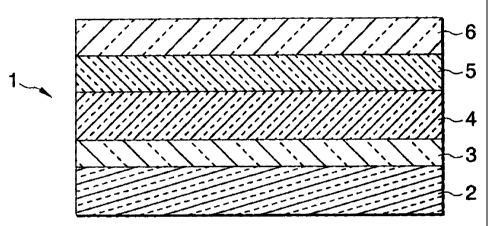
Fig. 1 is a sectional view of one embodiment of the
article having photocatalytic activity according to the present
invention.
Fig. 2 is an illustration showing an energy band
structure possessed by a multilayer structure according to the
present invention comprising a primer layer and a titanium oxide
photocatalyst film.
Fig. 3 is an illustration showing an energy band
structure near the surface of a conventional photocatalyst film
composed of a titanium oxide single layer and formed on a surface
of a substrate.
- 6a -
CA 02314381 2000-07-20
....,
In the drawings, the reference numerals are as follows.
1: Article of the present invention
2: Glass plate
3: Alkali dissolution preventive film of silicon
dioxide
4: Primer layer
5: Titanium oxide photocatalyst film
6: Hydrophilic film
DETAI:tED DESCRIPTION OF THE INVENTION
It is preferred in the present invention that the
photocatalyst film be constituted of either an oxide
semiconductor film made of titanium oxide (TiO2) (band gap: 3.0
eV in rutile, 3.2 eV in anatase) or an oxide semiconductor film
containing titanium oxide as the main component, from the
standpoint of enabling the film to have high photocatalytic
activity. Preferred examples of the photocatalyst film other
than such titaniuzn oxide films include a film of strontium
titanate (SrTiO3; band gap, 3.2 eV).
Besides being a t:itanium oxide film, the photocatalyst
film may be one comprising fine titanium oxide particles
dispersed in, e.g., a film of silicon dioxide.
The primer layer used in the present invention is
preferably constituted of an oxide semiconductor film
comprising at least one metal oxide selected from the group
consisting of niobium oxide (Nb2O5: 3.4 eV), tin oxide (SnOZ:
3.5 eV), aluminum oxide (A1203: >5 eV), zinc oxide (ZnO: 3.3
eV) and zirconium oxide (ZrO2: 5.0 eV).
- 7 -
CA 02314381 2000-07-20
..,.,
The thickness of the primer layer is preferably 5 nm
or larger. This is because thickness thereof smaller than 5
nm results in insufficient bonding to the photocatalyst film
due to a tunnelinq effect and hence in insufficient supply of
holes to the surface of the photocatalyst film.
The thickness of the photocatalyst film is preferably
30 nm or larger, more preferably 50 nm or larger. This is
because thickness thereof smaller than 30 nm results in
insufficient light absorption. On the other hand, the upper
limit of the thickness of the photocatalyst film is preferably
2,000 nm. This is because thickness thereof exceeding 2,000
nm results in relatively reduced bonding to the primer layer
and hence in insufficient effect of the deposition of the primer
layer. . From these standpoints, the thickness of the
photocatalyst fili-n is preferably 1,000 nm or smaller.
DESCRIPTION OF THE PREFERRED EMBODIMENTS
Embodiments of the present invention will be explained
in detail below :by reference to Examples and Comparative
Examples.
Fig. 1 is a sectional view of one embodiment of the
article having phoi:ocatalytic activity according to the present
invention. This article 1 having photocatalytic activity
comprises a glass plate 2 as a substrate and, superposed on a
surface thereof, a silicon dioxide film 3 as an alkali
dissolution preventive film, an n-type semiconductor film 4 as
a primer layer, a photocatalyst film 5, and a silicon dioxide
film 6 as a hydrophilic film. The primer layer 4 and the
~
- o -
CA 02314381 2000-07-20
photocatalyst film 5 are essential films, while the alkali
dissolution preventive film 3 and the hydrophilic film 6 are
optional films.
Fig. 2 is an illustration showing an energy band
structure possessed by a multilayer structure according to the
present invention comprising a primer layer (metal oxide;
indicated by MOX) and a ti tanium oxide photocatalyst film (TiOZ) .
Fig. 3 is an illustration showing an energy band
structure near the surface of a conventional photocatalyst film
composed of a titanium oxide single,layer and deposited on a
surface of a substrate.
As shown in Fig. 2, the energy level of the valence band
changes at the interface between the n-type semiconductor as
the primer layer and the titanium oxide photocatalyst film, and
the curve of energy level for the valence band is inflected so
that the surface of the photocatalyst film has an elevated
energy level. On the other hand, since the primer layer is
constituted of an n-type semiconductor film and bonded to the
photocatalyst film, the lower edge of the conduction band in
an inner part of the film has a slightly higher energy than the
Fermi level and the curve of energy level for the conduction
band is inflected so that the energy becomes high in a region
near the photocatalyst film surface as the position becomes
closer to the phot.ocatalyst film surface.
The article of the present invention has the above-
described inflections in energy level curve respectively at the
interface between the primer layer and the photocatalyst film
- Q -
CA 02314381 2000-07-20
and near the photocatalyst film surface. Consequently, the
article of the present invention is characterized by the
behaviors of holes and electrons in the film depth direction.
Namely, the energy-level holes h' present in the valence band
are apt to travel toward the photocatalyst film surface, while
the energy-level electrons e- present in the conduction band
are apt to travel toward an inner part of the photocatalyst film.
Because of this, the holes which have been generated
by charge separation are apt to travel toward the surface of
the photocatalyst film as shown in Fig. 2. The article of the
present invention is prevented from suffering the phenomenon
in which electrons recombine with holes inside the film to
result in charge ciisappearance and to come not to contribute
to photocatalytic activity, as compared with the case shown in
Fig. 3, wherein a single-layer photocatalyst film is formed.
The substi~ate used in the present invention is not
particularly limited. Optically, the substrate may be
transparent or opaque. Usable examples of the material of the
substrate include metals, ceramics, glasses and plastics.
When a transparent silicate glass plate, e.g. , a glass
plate manufactured by the float process, is used as the
substrate, a window glass having stain resistance can be
obtained.
Many silicate glasses usually contain an alkali
component such as sodium or potassium so as to secure
meltability, molda:bility into plate, etc. In the case of using
a glass plate containing an alkali component, it is preferred
- 10 -
CA 02314381 2000-07-20
to interpose an alkali diffusion preventive film between the
glass plate and the primer layer to thereby prevent the alkali
component from diffusing into the photocatalyst film.
Examples of this alkali diffusion preventive film include a
silicon dioxide film, silicon nitride film and silicon
oxynitride film. Films of other metal oxides are also usable.
The metal oxide film made of niobium oxide, tin oxide,
aluminum oxide, zinc oxide or zirconium oxide, which is
preferred for use as the primer layer in the present invention,
in itself has the ability to prevent alkali dissolution.'
The depos_Ltion of an alkali dissolution preventive film
is effective in preventing an alkali component from diffusing,
upon substrate heating in photocatalyst film formation, into
the photocatalyst film to impair the crystallinity of the
photocatalyst film or disorder the electron structure thereof.
Thus, photocatalytic act:ivity can be more effectively prevented
from decreasing.
In the present invention, a hydrophilic film can be
formed on the surface of the photocatalyst film. By the
formation of the hydrophilic film, enhanced hydrophilicity can
be imparted to the surface of the photocatalyst film. This
hydrophilic film preferably has a thickness so as not to impair
photocatalytic activity. From this standpoint, the thickness
thereof is generally 2C) nm or smaller, preferably 10 nm or
smaller, more preferably 5 nm or smaller. The hydrophilic film
may be formed so as to cover all or part of the photocatalyst
film. The hydrophilic film is not particularly limited in
- 11 -
CA 02314381 2000-07-20
material as long as it is hydrophilic, and preferred examples
thereof include films of silicon oxide, aluminum oxide, cerium
oxide and zirconium oxide.
In ordex= to enhance photocatalytic activity and
hydrophilicity, the article may be made to have surface
roughness by form:Lng any of the primer layer, photocatalyst film,
and hydrophilic :Eilm so as to have a roughened surface.
In Examples 1 to 5, a primer layer and a photocatalyst
film were formed by magnetron sputtering. Common formation
conditions are shown below. The methods used for evaluating
the photocatalyst films obtained are shown below.
Formation Conditions
Glass plate: Soda-lime silicate glass plate (15 cm x
15 cm; thickness, 2 mm)
Glass plate temperature during layer and film
formation: 350 C
Target: Metal target having dimensions of 25 cm x 38
cm x 6 mm (In fornzing niobium oxide primer film, niobium metal
was used as target.)
Power: 3 kW from direct-current power source
Sputtering gas atmosphere: Reactive sputtering in an
atmosphere maintained at 0.4 Pa by introducing oxygen gas
Evaluation Methods
Triolein-decomposing activity:
The surfac:e of ttie film was coated with 2. 5 g of triolein
(coating area: 25 cm2), and the coated surface was irradiated
with black light (ultraviolet ray) at an intensity of 3 mW/cm2
- 12 -
CA 02314381 2000-07-20
for 40 hours. The amount of the applied triolein which remained
undecomposed on the film surface was measured to determine the
residual amount thereof (wt%).
Contact angle: The film surface was irradiated with
black light (ultraviolet) at an intensity of 3 mW/cmz for 1 hour.
Immediately thereafter, the contact angle with pure water was
measured with a waterdrop contact angle meter.
Antifouling performance: Relative evaluation was
conducted with respect to fouled state resulting from 2-month
outdoor exposure
O: Obviously less fouled than a glass (having no
photocatalyst film) exposed simultaneously
0: Less fouled, under some conditions such as southward
exposure, than a cilass (having no photocatalyst film) exposed
simultaneously
x: Almost equal in fouling to a glass (having no
photocatalyst film) exposed simultaneously, and no difference
was observed therebetween
EXAMPLE 1
A soda-lime silicate glass plate was sufficiently
cleaned, heated to 350 C, and then coated on one side with a
primer layer of niobiuni oxide in a thickness of 50 nm. The
primer layer was formed by reactive sputtering using niobium
metal as a target while introducing oxygen gas into the film
formation chamber at a rate of 50 sccm. The surface of this
primer layer was coated with a photocatalyst film of titanium
oxide in a thickness of 250 nm. The titanium oxide film was
- 13 -
CA 02314381 2000-07-20
formed by reactive sputtering using titanium metal as a target
while introducinq an argon/oxygen mixed gas at a rate of 50 sccm.
Thus, Sample 1 was obtained as an example of the article of the
present inventiori havir.ig a photocatalyst film coating. Sample
1 was evaluated for the performances, and the results obtained
are shown in Table 1. The samples shown in Table 1, when
analyzed by the }C-ray diffraction method, each showed a peak
attributable to anatase crystals, and no difference in
crystallinity was observed among these.
Samples 2 to 5 were obtained using different primer
layer materials, and the evaluation results therefor are shown
in Table 1.
Table 1
Sample Multilayer structure Titanium oxide Triolein- Contact Anti-
No. Primer layer photocatalyst decom- angle fouling
Ingredient Thickness film posing with perfor-
Thickness activity water mance
(run) (residual (degree)
amount,%-)
(Example)
Sample 1 Nb205 50 250 0 9 00
Sample 2 A1203 50 250 0 10 Qo
Sample 3 SnOz 50 250 58 18 0
Sample 4 ZrO2 50 250 54 18 0
Sample 5 Zn0 50 250 35 14 @
(Compara-
tive Ex-
anp le)
compara- None 250 74 25 X
tive
Sample 1
- 14 -
CA 02314381 2000-07-20
CQMPARATIVE EXAMPLE 1
A photocatalyst film of titanium oxide was formed on
a glass plate in 1=he same manner as in Example 1, except that
the primer layer was omitted. Thus, Comparative Sample 1 was
produced. The film was tested, and the results obtained are
shown in Table 1 above.
Table 1 shows that the formation of the primer layers
results in decreases in triolein residual amount, which
indicates triolein-decomposing ability, and hence in enhanced
photocatalytic activity. It can be said that the enhanced
photocatalytic activity increases the hydrophilicity of the
film surface and irnparts antifouling performance. The results
for Samples 1 to 5 show that use of niobium oxide, aluminum oxide
or zinc oxide as a primer layer results in higher photocatalytic
activity of the photocatalyst film and hence in better
antifouling properties. It was found that the most preferred
primer materials aimong those are niobium oxide and aluminum
oxide from the standpoint of imparting such performances.
EXAMPLE 2
The same procedure as in Example 1 was conducted, except
that a niobium oxide film was formed as a primer layer in
different thicknesses. Thus, Samples 6 to 8 were produced to
examine the influence of" primer layer thickness on catalytic
activity. The evaluation results for the films are shown in
Table 2.
- 15 -
CA 02314381 2000-07-20
Table 2
Sample Multilayer structure Titanium oxide Triolein- Contact Anti-
No. Primer layer photocatalyst decom- angle fouling
Ingredient Thickness film, posing with perfor-
(nm) Thickness activity water mance
(nm) (residual (degree)
amount,%)
(Example)
Sample 6 Nbz05 20 250 0 10 Qo
Sample 7 Ntb205 10 250 0 9 Q
Sample 8 Nb2O5 5 250 0 9 oQ
(Compara-
tive Ex-
ample)
compara- Nb205 1 250 77 25 X
tive
Sample 2
COMPARATIVE EXAMPLE 2
The same procedure as in Example 1 was conducted, except
that a niobium oxide film was formed as a primer layer in a
different thickness. Thus, Comparative Sample 2 was produced.
The evaluation results for the film are shown in Table 2 above.
Table 2 shows that formation of the primer layer in a thickness
not smaller than 5 nm results in a reduced residual triolein
amount and sati sf actory antifouling properties. These results
in combination with the results for Sample 1 show that the
residual triolein amount was not influenced by the thickness
of the primer layer in the range of from 5 to 25 nm, and that
the primer layer almost fully produced its effect when it had
a thickness as small as 5 nm. Practically, the thickness
thereof may be 3 nm. In contrast, when the primer layer
- 16 -
CA 02314381 2000-07-20
thickness was 1 nm or smaller, the primer layer was ineffective
in improving the activity of the photocatalyst film as in
Comparative Sample 2.
EXAMPLE 3
The same procedure as in Example 1 was conducted, except
that the temperature of the glass plate in the formation of a
50-nm niobium oxide film as a primer layer and a 250-nm titanium
oxide film as a photocatalyst film in a multilayer constitution
was changed. Thus, Samples 9 to 12 were produced. The
evaluation results obtained are shown in Table 3.
Table 3
Sample No. Glass temperature in Triolein- Contact Anti-fouling
photocata3.yst filin decoaposing angle performance
formation activity with
( C:) (residual water
amount, %) (degree)
(Example)
Sample 9 300 0 10 oQ
Sample 10 250 4 11 Q
Sample 11 150 12 12 0
Sample 12 No hea.ting 34 15 0
Table 3 shows that by forming the primer layer,
photocatalytic activity can be obtained without heating the
glass plate. This means that even in the case of using a
substrate made of an organic resin having relatively poor
thermal resistance, photocatalytic activity can be imparted to
a surface of the substrate without deteriorating the substrate.
Samples 9 to 12 each showed an X-ray diffraction peak
- 17 -
CA 02314381 2000-07-20
attributable to anatase crystals, although they varied in peak
intensity.
EXAMPLE 4
The same procedure as in Example 1 was conducted, except
that the thickness of the photocatalyst film was changed. Thus,
Samples 13 to 16 we:re produced. The evaluation results obtained
are shown in Table 4.
CQIYIPARATIVE EXAMPLE 3
The same p:rocedure as in Example 1 was conducted, except
that the thickness of the photocatalysj: film was changed. Thus,
Comparative Sample 3 waas produced. The evaluation results
obtained are shown in Table 4.
Table 4
Sample No. Multilayer structure Titanium Triolein- Contact Anti-
Primer layer oxide photo- decom- angle fouling
Ingredient 'rhickness catalyst posing with perfor-
(nm) film, activity water mance
Thickness (residual (degree)
(nm) amount, %)
(Example)
Sample 13 Nbz05 50 200 0 9 Qo
Sample 14 Nb205 50 150 8 11 @
Sample 15 Nb205 50 50 17 13 0
Sample 16 NbZ05 50 30 36 15 O
(Compara-
tive
Example)
Compara- Nb205 50 15 87 24 X
tive
Sample 3
_ 1R -
CA 02314381 2000-07-20
Table 4 shows that the thickness of the photocatalyst
film is preferably 30 nm or larger, more preferably 50 nm or
larger. On the other hand, when the thickness thereof was 15
nm, almost no photocatalytic function was obtained.
EXAMPLE 5
An SiO2 film having a thickness of 20 nm was formed as
an alkali dissolution preventive film by high-frequency
sputtering using quartz glass as a target. Thereafter, a primer
layer and a photocatalyst film were formed successively on the
alkali dissolution preventive film in the same manner as in
Example 1. Thus, Sample 17 was produced. Furthermore, Sample
18 was produced by forming a hydrophilic film of SiO2 having
a thickness of 10 nm on the photocatalyst film. The test results
for these films ai-e shown in Table 5. Sample 18 had improved
surface hydrophi_licity although slightly reduced in
photocatalytic activity as determined through the triolein
decomposition test. Sarriple 17, which had an alkali dissolution
preventive film, was almost equal to Sample 1 in triolein-
decomposing activity and contact angle with water
(hydrophilicity).
- 19 -
CA 02314381 2000-07-20
Table 5
Sample Alkali Primer Photo- Hydro- Triolein- Contact Anti-
No. disso- layer catalyst philic decom- angle fouling
lution film film posing with perfor-
pre- activity water mance
ventive (residual (degree)
film amount, $)
(Example)
Sample 17 SiOZ Nb205 Ti02 0 9 ~O
(20) (50) (250)
Sample 18 SiOZ N10205 Ti02 Si0Z 14 7 ~o
(20) (50) (250) (10)
Note 1: The numeral in each parenthesis, indicates thickness (nm)
EXAMPLE 6
A tin oxida film having a thickness of 600 nm was formed
as a primer layer on a heated glass plate having a soda-lime
silicate composition by CVD (chemical vapor deposition) using
dibutyltin dichlor=ide as a starting material. On this coating
film was formed a titani_um oxide photocatalyst film having a
thickness of 60 nm by the sol-gel method using a coating liquid
containing titanium tetraisopropoxide. Thus, Sample 19 was
produced. The coating liquid was prepared by chelating 0.032
mol of titanium tetraisopropoxide with 0.064 mol of
acetylacetate and adding 93 ml of ethanol and 0. 004 mol of acetic
acid to the chelate. The titanium oxide film was formed by
dipping the glass plate in this coating liquid, pulling up the
glass plate (pulling rate, 9.0 mm/sec), and then burning the
coating at 500 C for 30 minutes. The photocatalytic activity
of sample 19 was evaluated through various oxidation reactions
and reduction reactions. The results obtained are shown in
- 20 -
CA 02314381 2000-07-20
...,.
Table 6. The thus-obtained titanium oxide film of Sample 19
contained anatase crystals, and the diffraction peak intensity
for the (101) plarie of the anatase crystals was 12.6, which was
on almost the same level as that in Comparative Sample 4(13.2) .
Table 6
Sample 19 Compara-
tive
Sample 4
1) Rate of oxidative photodecomposition of formic acid 4.1 1.3
(10-6 mol/hr)
2) Rate of oxidative photodecomposition of 1.7 0.6
1,3,5,7-tetramethylcycloi:etrasiloxane
monomolecular film (degree/min)
3) Degree of oxidative! decomposition of oleic acid (~) 70.6 34.7
(light irradiation: 168 hours)
4) Rate of oxidative decomposition of acetaldehyde 43.4 29.2
(ppm/hr)
5) Rate of silver precipitation through 0.83 1.4
photoreduction (10-' mol/hr)
6) Rate of photoreduction of bis(2-dipyridyl) 0.71 1.1
disulfide to 2-mercaptopyridine (10-4 mol/hr)
7) Crystals of titanium oxide film Anatase Anatase
8) Intensity for (101) plane of anatase crystals 12.6 13.2 0.6
(arbitrary unit)
CQMPAF2ATIVE EXAMPLE 4
The same p:rocedure as in Example 6 was conducted, except
that the tin oxide primer layer was omitted and the glass plate
was replaced with. a quartz glass plate. Thus, Comparative
Sample 4 was produc:ed, which consisted of the quartz glass plate
and a titanium oxicie photocatalyst film deposited thereon. The
test results for the film obtained are shown in Table 6. The
titanium oxide film of Comparative Sample 4 obtained also
contained anatase crystals and had slightly satisfactory
crystallinity. The film was thought to be partly amorphous and
partly crystalline.
The photocatalyst film of Sample 19, which had a primer
- 21 -
CA 02314381 2000-07-20
layer, showed higher rates of oxidation reactions 1) to 4) than
the photocatalyst:film of Comparative Sample 4 but had lower
rates of reduction. reactions 5) and 6) than the comparative film.
For enhancing the property of preventing the fouling caused by
adherent organic substances, etc. , it is important to heighten
the rates of oxidative decomposition reactions. From this
standpoint, the photoca.talyst film of Sample 19 according to
the invention was found to have excellent antifouling
properties.
EXAMPLE 7
A soda-lime silicate glass plate was coated by the
sol-gel method with a three-layer coating composed of a silicon
dioxide film as an alkali dissolution preventive film, a tin
dioxide film as a primer layer, and a titanium oxide film as
a photocatalyst f'ilm. Thus, Sample 20 was produced. The
photocatalyst film obtained was tested for catalytic activity
in the oxidative decomposition reaction of Acid Blue 9. The
results obtained are shown in Table 7.
Sample 21 was further produced by coating a soda-lime
silicate glass plate by the sol-gel method with a three-layer
coating composed of a silicon dioxide film as an alkali
dissolution preventive film, a zirconium oxide film as a primer
layer, and a titanium oxide film as a photocatalyst film. This
photocatalyst film was examined in the same manner, and the test
results obtained ai-e shown in Table 7. Details of the procedure
of Sample 20 production are as follows.
The silicon dioxide film was formed by preparing a
- 22 -
CA 02314381 2000-07-20
,.-..
coating fluid using tetraethoxysilane as a starting material,
applying the coating fluid by spin coating (1,500 rpm),
predrying the coating at 320 C for 5 minutes, and then burning
it at 500 C for 1 hour.
The tin oxide film was formed by adding 1.59 g of
acetylacetone and 25.62 g of ethyl Cellosolve to 2.79 g of
stannic chloride hydrate to prepare a coating liquid, applying
the coating fluid by spin coating (1,500 rpm), and drying the
coating at 320 C for 5 minutes.
The titanium oxide film was formed by adding 7.53 g of
acetylacetone and 41.79 g of ethyl Cellosolve to 10.68 g of
titanium isopropoxide to prepare a coating fluid, applying the
coating liquid by spin coating on the surface of the tin oxide
film which had been dried at 320 C, predrying the coating at
320 C for 5 minutes, and then burning it at 620 C for 6 minutes.
The alkali. dissolution preventive film and titanium
oxide film of Sample 21 were deposited in the same manners as
for"Sample 20.
The zircon.ium oxide film was formed by adding 5.07 g
of ethyl acetoacetate and 47.46 g of ethyl Cellosolve to 7.47
g of zirconium tetrabutoxide to prepare a coating liquid and
drying the applied coating liquid at 320 C for 5 minutes.
For evaluziting catalytic activity in an oxidation
reaction thought to contribute to fouling prevention, a test
liquid was used which had been prepared by dispersing Acid Blue
9, an organic pigment, _Lnto poly(vinyl alcohol) This test
liquid was applied on the surface of the photocatalyst film by
- 23 -
CA 02314381 2000-07-20
spin coating and then irradiated with black light at 3 mW/cm2
for 10 minutes. From the difference between the absorbance
before the irradiation and that after it, the rate of oxidative
decomposition of Acid Blue 9 was determined.
COMPARATIVE EXAMPLE 5
The same procedure as for Sample 20 in Example 7 was
conducted, except. that the primer layer was omitted. Thus,
Comparative Sample 5 was produced. The film obtained was tested
in the same manner as in Example 7, and the results obtained
are shown in Tab:Le 7. The samples,shown in Table 7, when
analyzed by the X-ray d.iffraction method, each showed a peak
attributable to anatase crystals. In each of these X-ray
diffraction patterns, the peak attributable to anatase crystals
was broad, indicating that the crystallization was incomplete.
No difference was observed among these samples.
- 24 -
CA 02314381 2000-07-20
Table 7
Sample Alkali Primer Photo- Rate of
dissolution layer catalyst decomposi-
preventive film tion of Acid
film Blue 9
(relative
value)
(Example)
Sample 20 Si02 Sn02 Ti02 7.06
(10C)) (60) (90)
Sample 21 SiC)2 Zr02 Ti02 7.42
(100) (60) (90)
(Compara-
tive
Example)
Compara- Si0z - Ti02 4.11
tive
Sample 5 (100) (90)
Note 1: The numeral in each parenthesis indicates thickness
(nm).
Note 2: Each relative value is based on the decomposition rate
for comparative sample 6 in Table 8, which was taken
as 1.00.
Table 7 shows that the decomposition rate was increased
by forming a primer layer. Namely, it was found that
photocatalytic activity is improved by interposing a primer
layer between the glass plate and the photocatalyst film.
EXAMPLE 8
A silicon dioxide film as an alkali dissolution
preventive film was formed on a soda-lime silicate glass plate
by the sol-gel method. On this film was formed a tin oxide film
as a primer layer by the sol-gel method. A film consisting of
silicon dioxide as a matrix and fine titanium oxide particles
- 25 -
CA 02314381 2000-07-20
dispersed thereiri was further formed as a photocatalyst film
on the primer layer by the sol-gel method. Thus, Sample 22 was
produced, which had a three-layer coating.
Sample 23 having a three-layer coating was produced in
the same manner a:; for sample 22, except that the primer layer
was replaced with a zirconium oxide film. Furthermore, Sample
24 having a three-layer coating was produced in the same manner
as for Sample 22, except that the primer layer was replaced with
a niobium oxide film.
The silicon oxide film, tin oxide film, and zirconium
oxide film were deposited by the same methods as in Example 7.
The niobium oxide film was formed by applying coating fluid
GIP-NbO4-1 (trade name), manufactured by Giken Kagaku K.K., by
spin coating and drying the coating at 320 C for 5 minutes.
The photocatalyst film was deposited by mixing 6 g of
coating fluid ST-K03 (trade name) for photocatalyst deposition
(containing SiOZ and TiOZ in a ratio of 50:50 by weight),
manufactured by Ishihara. Sangyo Kaisha, Ltd. , with 9 g of ethyl
Cellosolve, applying the diluted coating fluid by spin coating,
preburning the coating at 320 C for 5 minutes, and then burning
it at 620 C for 6 minutes.
COMPARATIVE EXAMPLE 6
The same procedure as for Sample 22 in Example 8 was
conducted, except that the primer layer was omitted. Thus,
Comparative Sample 6 was produced, which had a two-layer coating.
The test results for the film obtained are shown in Table 8.
The samples shown in Table 8, when analyzed by the X-ray
- 26 -
CA 02314381 2000-07-20
,.-.
diffraction method, each showed a distinct diffraction peak
attributable to anatase crystals.
Table 8
Sample Alkali Primer Photocatalyst Rate of
disso- layer film decomposi-
lution tion of
pre- Acid
ventivea Blue 9
film (relative
value)
(Example) Si02 Sn02 Si02 containing dispersed 7.67
Sample 22 (100) (60) Ti02 particles
(120)
Sample 23 SiOZ Zr02 Sioz contai-ning dispersed 1.55
(100) (60) Ti02 particles
(120)
Sample 24 Si.02 Nb205 SiOZ containing dispersed 2.75
(100) (60) TiOZ particles
(120)
(Compara-
tive
Example)
Compara- SiOZ Sio2 containing dispersed 1.00
tive (100) TiOZ particles
Sample 6 (120)
Note 1: The numeral in each parenthesis indicates thickness
(nm).
Note 2: Each relative value is based on the decomposition rate
for comparative sample 6, which was taken as 1.00.
Table 8 shows that use of a thin, transparent silicon
dioxide film containing fine titanium oxide particles dispersed
therein as a photoc:atalyst film was also effective in improving
photocatalytic activity.
The article of the present invention has a multilayer
structure which comprises a substrate, a first n-type
- 27 -
CA 02314381 2000-07-20
.=-,
semiconductor film as a primer layer formed over a surface of
the substrate, and a photocatalyst film made of an n-type
semiconductor and formed on the primer layer, and in which the
first n-type semic:onductor film as the primer layer has a larger
energy band gap than the photocatalyst film. Due to this
constitution, holes are apt to move to areas near the surface
of the photocatalyst film, whereby electron/hole recombination
within the photocatalyst film is inhibited. Since electrons
and holes are thus inhibited from recombining and thereby coming
not to contribute to photocatalytic activity, the article has
photocatalytic functions effectively imparted thereto.
When an oxide semiconductor film comprising titanium
oxide is used as the photocatalyst film and an oxide
semiconductor filni comprising at least one metal oxide selected
from the group consisting of niobium oxide, tin oxide, aluminum
oxide, zinc oxide and zirconium oxide is used as the primer layer,
then photocatalytic activity can be ef fectively imparted to the
article.
When the thickness of the primer layer and that of the
photocatalyst filni are regulated to 5 nm or larger and to from
30 to 2,000 nm, respectively, then photocatalytic activity can
be effectively imparted to the article.
Furthermore, when the substrate is a transparent
silicate glass plate anci the article has, interposed between
the glass plate and the primer layer, an alkali diffusion
preventive film serving to prevent the alkali ingredient(s)
contained in the silicate glass from diffusing into the
_ ;~ g _
CA 02314381 2000-07-20
photocatalyst film, then photocatalytic activity can be
effectively imparted especially in the case where the substrate
is heated to a high temperature in forming the photocatalyst
film.
- 29 -